Structural and optical characterizations of GaN-based green light-emitting
diodes growth using TiN buffer layer
C. Y. Shieh
1, Z. Y. Li
2,
H. C. Kuo
2, G. C. Chi
1,21
Department of Optics and Photonics, National Central University. No.300, Jhongda Rd. , Jhongli
City, Taoyuan County 32001, Taiwan
2
Department of Photonics,National Chiao Tung University. No.1001 University Rd. , Hsinchu 300,
Taiwan
ABSTRACT
The present study investigated the structural and optical characterizations of the growth of GaN-based green light-emitting diodes using a TiN buffer layer. The purpose of growing GaN-based green LEDs on the TiN interlayer was to produce the naturally occurring hexagonal pattern structure on the surface of undoped-GaN. Then dislocations of the grown InGaN/GaN MQWs green LEDs structure on the uGaN template with the TiN interlayer produced base plane staking faults through epitaxial lateral overgrowth. Cross-section transmission electron microscope images showed that the dislocation density of green LEDs was decreased from 5 × 108 cm-2 to 7 × 107 cm-2, and that the dislocations in the
green LEDs structure were reproduced. The full widths at half maximum of the omega-scan rocking curves in (002) and (102) reflectance on the GaN-based green LEDs were 334 and 488 arcsec, respectively. As the injection current was increased from 5 mA to 40 mA, the electroluminescence peak wavelength of the GaN-based green LEDs was shifted from 508 nm to 481 nm, a blue-shift of 27 nm. The forward voltage measured at an injection current of 20 mA was 4.9 V for the GaN-based green LEDs according to the current-voltage characteristics. Due to an increase in the In mole fraction of the GaN-based green LEDs on the uGaN template with the TiN interlayer, the strain and phase separation were increased, and the multiple quantum wells structural quality and device performances of the GaN-based green LEDs were decayed. A yellow band with a wavelength of 551nm was thereby produced according to room temperature photoluminescence measurement. Meanwhile, cross-section transmission electron microscope images indicated V-defects in multiple quantum wells structures of the green LEDs.
Keywords: green LEDs, TiN, pattern structure, ELOG, dislocations, TEM, XRD, EL
1. INTRODUCTION
InGaN-based light-emitting semiconductor devices producing green wavelengths of 520 nm to 570 nm have attracted great interest in solid-state-lighting (SSL) and projection display applications [1-3]. The main challenge currently presented by InGaN-based green light-emitting diodes (LEDs) is that the efficiency drops rapidly as Indium (In) content increases in multiple quantum wells (MQWs) due to the internal electric field (IEF) increasing because of threading dislocations (TDs). This result is known as the “green gap” [4]. Efficiently reducing the TDs density (TDD) of the InGaN-based green LEDs’ structure is theorized to improve the material quality and increase quantum efficiency. The large differences of lattice constants and thermal expansion coefficients for grown highly luminescent InGaN-based green LEDs on sapphire substrates produced the high density (108 – 1010 cm-2) of TDs. When the TDs propagate from
c-plane GaN/sapphire interface to InGaN/GaN MQWs of green LEDs, the TDs could break continuous structures during the MQWs growth and cause defects in MQWs. Thus decreasing electron-hole overlap and making carriers reaching to defects reduced the radiative efficiency of InGaN-based LEDs [5]. To reduce the TDDs for InGaN-based epitaxial layers on sapphire substrate, the growth of InGaN-based LEDs on various material buffer layers significantly improves the structural quality and the radiative efficiency such as GaN [5], TiN microporous network templates [6], ScN [7], and CrN etc [8]. But the TDs of these techniques have been reduced to 108 cm-2 at undoped-GaN (u-GaN) template.
*Phone: +886-3-4227151ext 57915 Fax: +886-3-4258816 E-mail: [email protected]
Gallium Nitride Materials and Devices VIII, edited by Jen-Inn Chyi, Yasushi Nanishi, Hadis Morkoç, Joachim Piprek, Euijoon Yoon, Hiroshi Fujioka, Proc. of SPIE Vol. 8625, 862529 · © 2013 SPIE
CCC code: 0277-786X/13/$18 · doi: 10.1117/12.2004465
Proc. of SPIE Vol. 8625 862529-1
, ,
*t
a.J=
'
1
M
i
(c)
e
a
T_e(sice.^.d)In this study, we report the structural and optical characterizations of GaN-based green LEDs growth using TiN buffer layer. We grow the secondary phase crystal structure which cubic-TiN epilayer between LT-GaN buffer layer and sapphire and enhance a continuous step surface at uGaN template.
2. EXPERIMENT
In this study, we separately deposited titanium layers with 2 nm, 4 nm, 6 nm, 8 nm, and 10 nm thick layers on 2 inch (0001) c-plane sapphire wafers by E-Gun evaporator with a base-pressure 4 × 10⁻⁶ torr. Then these wafers formed a TiN
epilayer after nitridating under NH3 environment at 950 ℃ and later deposited a low-temperature (LT) at 520 ℃
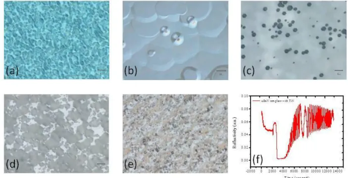
30-nm-thick GaN layer and a high-temperature (HT) at 1070 ℃ 4-μm-30-nm-thick undoped GaN (uGaN) layer on sapphire wafers in sequence by metal-organic chemical vapor deposition (MOCVD Veeco D75). Figure 1 (a-e) showed these uGaN templates with various thickness TiN epilayers by optical microscope (OM). We cheese the uGaN template with a 4-nm-thick TiN epilayer that has the continuous flat surface by OM images and in-situ monitoring result shown in figure (f) and then grew green LEDs structure on this uGaN template with a 4-nm-thick TiN epilayer by MOCVD.
Figure 1 shows uGaN template using TiN buffer layer with (a) 2 nm; (b) 4 nm; (c) 6 nm; (d) 8 nm; (e) 10 nm thickness and (f) in-situ monitoring of uGaN template using TiN buffer layer (4 nm).
The In0.32Ga0.68N/GaN MQWs green LEDs samples used in this study were re-grown by MOCVD on uGaN template
with TiN buffer layer. For the growth of the InGaN epilayers, trimethylgallium (TMGa), trimethylindium (TMIn), trimethylaluminum (TMAl), and ammonia (NH3) were used as Ga, In, Al, and N sources, respectively. Silane (SiH4) and
bis (cyclopentadienyl) magnesium (Cp2Mg) were used for n-type and p-type dopings, respectively. The green LEDs
structure consisted of a 2.5-μm-thick Si-doped n-type GaN (n-GaN) epilayer, an InGaN/GaN MQWs active layer, a 20-nm-thick Mg-doped Al0.2Ga0.8N as the electron blocking layer, a 5-nm-thick p-plus GaN, and finally a 200-nm-thick
Mg-doped p-type GaN (p-GaN) cap layer. The MQWs active layer consisted of ten periods of 2-nm-thick InGaN well layers and 10-nm-thick GaN barrier layers. For the green LEDs samples fabrication, a 180-nm-thick indium tin oxide (ITO) film was first deposited on the green LEDs samples as a transparent contact layer (TCL). Then partially etching the surface of the green LEDs samples until 1.5 μm depth of the n-GaN layer were exposed. We subsequently deposited Cr/Pt/Au (50nm/50nm/150nm) onto the exposed n-GaN and p-GaN layer to serve as the n-type and p-type electrode. The chip size of green LEDs samples was 300 × 300 μm2.
The structural characterizations of GaN-based green LEDs growth using TiN buffer layer were analyzed by high resolution transmission electron microscopy (HRTEM), field emission scanning electron microscope (SEM) and high resolution X-ray diffraction (HRXRD) method using Cu Kα1 (λ=1.54056 Α) as source. The optical characterizations of this sample were investigated by electroluminescence (EL) and photoluminescence (PL) measurements, which were
Proc. of SPIE Vol. 8625 862529-2
characteristics of the GaN-based green LEDs were also measured using the molded green LEDs with the integrated sphere detector.
3. RESULTS AND DISCUSSION
The continuous, step 4-μm-thick HT-GaN layers found to be successfully formed on the LT-GaN and sapphire shown in Fig. 1 (b). And grown HT-GaN layers using TiN buffer layer was produced the naturally hexagonal micro-pattern structure which its diameter was 15 to 30 μm on the surface of undoped-GaN. The structural characterizations of GaN-based green LEDs with TiN buffer layer are illustrated in Fig. 2 by HRTEM. Fig. 2 (a) showed a typical TEM cross-sectional image of GaN-based green LEDs samples. We observed that many horizontal stacking faults were produced at n-type GaN layer and HT-GaN layer interface. These horizontal stacking faults at n-GaN layer blocked TDs from sapphire propagating to MQWs of GaN-based green LEDs. The TDD of GaN-based green LEDs was decreasing from 5x108 cm-2 to 7x107 cm-2 at n-GaN layer. The observation was attributed to GaN-based green LEDs structure growth on
uGaN template by epitaxial lateral overgrowth (ELOG). But the TDs in the green LEDs structure were reproduced due to high In content when InGaN/GaN MQWs growth produced V-defects shown in Fig. 2 (b). Most of the V-defects originate from the intersection of dislocations with InGaN/GaN MQWs, where large strain promotes their formation [9-10].
Figure 2 shows (a) the all LEDs structure at g = 0002 and (b) MQWs of GaN-based green LEDs with TiN buffer layer by HRTEM.
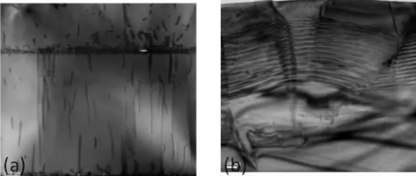
Fig. 3 (a) showed the TiN buffer layer which 4-nm-thick on sapphire via nitridating under NH3 environment at 950 ℃.
The 4-nm-thick hexagonal titanium layer by E-gun evaporator could burn over 882 ℃ and form cubic-TiN epilayer via nitridating in early study. From TEM we observed fuzzy image between TiN and sapphire and slip system in TiN layer. The results were also shown in Fig. 3 (b) by SEM that had several slip-lines at GaN epilayers/sapphire interface. Thus we objected a continuous, step structure on uGaN template with TiN buffer layer shown in Fig. 1 (b).
Figure 3 (a) shows the HT-GaN/LT-GaN/TiN buffer layer and sapphire interface by HRTEM and (b) all LEDs structure at g = 0002 by SEM.
excited with the 325 nm line of a He–Cd laser at excitation power densities of 20 mW. We measured their RT current-voltage (I-V) characteristics by an HP4156 semiconductor parameter analyzer. Light output power-current (L-I)
Proc. of SPIE Vol. 8625 862529-3
(a)
zorr, 30,4 II. 40,4 35C 4CC 47:: 500 5!0 60 EL wareleneth 02621 E. 0.00 0.02 0.04 0.06 0.08 0.10 Current (A) .6000 .5000 -.4000s- -.3000 "0 .2000 1620 54Fig. 4 shows the X-ray diffraction results of GaN-based green LEDs using TiN buffer layer. In wurtzite GaN films, the full width at half maximum (FWHM) of the (002) –rocking curve is associated with the density of screw or mix dislocations, while the FWHM of the (102) –rocking curve is affected by all dislocations [11]. As shown in Fig. 4, the FWHM of the (002) and the (102) – rocking curve are 334 and 488 arcsec. The edge dislocations that are horizontal stacking faults due to slipping by n-GaN epilayers in this study block TDs propagating to MQWs. Thus the edge dislocations at n-GaN epilayers are regard as decreasing TDD factor.
-2000 -1000 0 1000 2000 0.0 0.2 0.4 0.6 0.8 1.0 N o r m a li z e d X R D i n te n si ty ( a .u .)
Rucking curve (arcsec)
(002) Green LEDs TiN
(102) Green LEDs TiN
Figure 4 shows the (002) and (102) rucking curves of GaN-based green LEDs with TiN buffer layer by HRXRD.
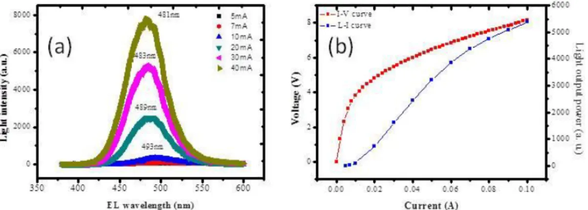
Fig. 5 (a) shows the electroluminescence (EL) spectra of GaN-based green LEDs with TiN buffer layer at increasing pulsed currents from 5 mA to 40 mA. As the injection current increases from 5 mA to 40 mA, the EL peak wavelength of the GaN-based green LEDs shifts from 508 nm to 481 nm blue-shifted for 27 nm. The current-induced blue shift, accompanied by a significant spectrum broadening, occurs mainly due to band filling of localized states originating from compositional fluctuation of InGaN alloys. Fig. 5 (b) shows the current-voltage (I-V) and light-output-power-current (L-I) characteristics of GaN-based green LEDs. The measured forward voltage at an injection current of 20 mA is 4.9 V for GaN-based green LEDs from the current-voltage characteristics. The junction leakage current in the green LEDs with TiN buffer layer at a reverse bias of -5 V is 1.075 mA.
Figure 5shows (a) EL and (b) L-I-V measurement of GaN-based green LEDs with TiN buffer layer.
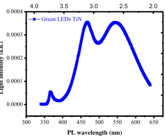
Fig. 6 shows room-temperature PL spectra of the green LED using TiN buffer layer. It was found that we could observe a band-edge (BE) emission at around 366 nm, a blue-band (BB) emission at around 468 nm, and a green-yellow-band (GYB) emission at around 551 nm from this sample. We are able to demonstrate white luminescence by light mixing from BB and GYB of InGaN/GaN MQWs in PL measurement experiment. Due to the In mole fraction of GaN-based green LEDs on uGaN template with TiN interlayer increasing, the strain and phase separation increase, the multiple quantum wells structure quality and device performances of GaN-based green LEDs can decay. V-defects in MQWs are shown in Fig. 2 (b) by HRTEM and we observe MQWs structures are bent by V-defects and cut by TD. Thus the In content distribution in MQWs is not uniform. Green band was produced the BB and GYB by phase separation due to V-defects in MQWs from RTPL measurement.
Proc. of SPIE Vol. 8625 862529-4
300 350 400 450 500 550 600 650 0.0000 0.0001 0.0002 0.0003 0.0004 L ig h t i n te n si ty (a .u .) PL wavelength (nm)
Green LEDs TiN
4.0 3.5 3.0 2.5 2.0
Figure 6 shows PL intensity of GaN-based green LEDs with TiN buffer layer.
4. SUMMARY
Although the threading dislocations density of GaN-based green LEDs using TiN nano-masks layer and epitaxial lateral overgrowth was decreased to 7 × 107 cm-2. But the performances of GaN-based green LEDs was not so good. Due to the
In mole fraction of GaN-based green LEDs on uGaN/TiN/sapphire increasing, the strain and phase separation increase, the multiple quantum wells structure quality and device performances of GaN-based green LEDs can decay. It was produced the yellow band that the wavelength was 551 nm from room temperature photoluminescence measurement. Meanwhile cross-section transmission electron microscope observed V-defects from multiple quantum wells structure of green LEDs.
REFERENCES
[1] K. S. Kim, J. K. Son, S. N. Lee, Y. J. Sung, H. S. Paek, H. K. Kim, M. Y. Kim, K. H. Ha, H. Y. Ryu, O. H. Nam, “Characteristics of long wavelength InGaN quantum well laser diodes”, Appl. Phys. Lett. 92, 101103 (2008).
[2] D. Queren, A. Avramescu, G. Bruderl, A. Breidenassel, M. Schillgalies, S. Lutgen, U. StrauB, “500 nm electrically driven InGaN based laser diodes”, Appl. Phys. Lett. 94, 081119 (2009).
[3] T. Miyoshi, S. Masui, T. Okada, T. Yanamoto, T. Kozaki, S. I. Nagahama, T. Mukai, “510–515 nm InGaN-Based Green Laser Diodes on c-Plane GaN Substrate”, Appl. Phys. Express 2, 062201 (2009).
[4] M. V. Durnev, A. V. Omelchenko, E. V. Yakovlev, I. Y. Evstrtov, S. Y. Karpov, “Strain effects on indium incorporation and optical transitions in green-light InGaN heterostructures of different orientations”, Phys. Status Solidi A 208, 2671 (2011).
[5] S.Nakamura, J. pearton G. Fasol, [The Blue Laser Diode: The Complete Story], 2nd edition, Springer Verlag;
(2000).
[6] U. Ozgur, Y. Fu, Y.T. Moon, F. Yun, H. Morkoc, H.O. Everitt, S.S. Park, K.Y. Lee, “Long carrier lifetimes in GaN epitaxial layers grown using TiN porous network templates”, Appl. Phys. Lett. 86, 232106 (2005).
[7] M. A. Moram, Y. Zhang, M. J. Kappers, Z. H. Barber, and C. J. Humphreys, “Dislocation reduction in gallium nitride films using scandium nitride interlayers”, Appl. Phys. Lett. 91, 152101 (2007).
[8] J. S. Ha, H. J. Lee, S. W. Lee, H. J. Lee, S. H. Lee, H. Goto, M. W. Cho, T. Yao, S. K. Hong, R. Toba, J. W. Lee, and J. Y. Lee, “Reduction of dislocations in GaN films on AlN/sapphire templates using CrN nanoislands”, Appl. Phys. Lett. 92, 091906 (2008).
[9] D. I. Florescu, S. M. Ting, J. C. Ramer, D. S. Lee, V. N. Merai, A. Parkeh, D. Lu, E. A. Armour, L. Chernyak, “Investigation of V-Defects and embedded inclusions in InGaN/GaN multiple quantum wells grown by metalorganic chemical vapor deposition on (0001) sapphire”, Appl. Phys. Lett. 83, 33 (2003).
[10] X. H. Wu, C. R. Elass, A. Abare, M. Mack, S. Keller, P. M. Petroff, S. P. DenBaars, J. S. Speck, “Structural origin of V-defects and correlation with localized excitonic centers in InGaN/GaN multiple quantum wells”, Appl. Phys. Lett. 72, 692 (1998).
[11] B. Heying, X. H. Wu, S. Keller, Y. Li, D. Kapolnek, B. P. Keller, S. P. DenBaar, J. S. Speck, “Role of threading dislocation structure on the x‐ray diffraction peak widths in epitaxial GaN films”, Appl. Phys. Lett. 68, 643 (1996).
Proc. of SPIE Vol. 8625 862529-5