國立交通大學
電子工程學系 電子研究所碩士班
碩士論文
利用溶膠法沉積高介電常數材料
捕陷電荷層之 SONOS 型記憶體元件
SONOS-Type Memory Devices with High-K
Dielectrics as Charge Trapping Layer by
Sol-Gel Spin Coating Deposition
研究生:徐梓翔
指導教授:雷添福 博士
利用溶膠法沉積高介電常數材料
捕陷電荷層之 SONOS 型記憶體元件
SONOS-Type Memory Devices with High-k
Dielectrics as Charge Trapping Layer by
Sol-Gel Spin Coating Deposition
研 究 生:徐梓翔 Student: Tzu Hsiang Hsu 指導教授:雷添福 博士 Advisor: Dr. Tan-Fu Lei
國 立 交 通 大 學
電子工程學系 電子研究所碩士班
碩士論文
A Thesis
Submitted to Department of Electronics Engineering & Institute of Electronics College of Electrical and Computer Engineering
National Chiao Tung University In Partial Fulfillment of the Requirements
For the Degree of Master of Science
in
Electronic Engineering June 2006
Hsinchu Taiwan Republic of China
利用溶膠法沉積高介電常數材料
捕陷電荷層之 SONOS 型記憶體元件
學生 :徐 梓 翔 指導教授: 雷 添 福 博士
國立交通大學
電子工程學系 電子研究所碩士班
摘要
傳統浮停閘結構的快閃記憶體,當元件的穿隧氧化層厚度小於 10 奈米時, 原本儲存在複晶矽浮停閘的電荷,很容易因為在氧化層的缺陷,形成漏電路徑, 造成原本儲存的資料流失。因此 SONOS 結構的記憶體元件,被提出是可以解決當 元件尺寸縮小時,浮停閘結構所面對的問題。傳統 SONOS 結構的記憶體元件,是 使用氮化矽作為電荷陷捕層,在此種結構內,因為電荷是被儲存在分離式的陷捕 位置中,故可改善在浮停閘結構中對於資料保存性的問題。但是因為氮化矽與穿 隧氧化層之間的導電帶位能差太低,會使得元件的寫入、抹除速度降低,因此使 用高介電常數材料作為 SONOS 結構的陷捕電荷層,目前正被廣泛研究著。 一般沉積高介電常數材料的方法有許多種,如:原子層沉積法、物理氣象沉 積法(濺鍍)、金屬有機沉積法,但是上述的方法所需要的成本相當昂貴。而在本 篇論文中則提出了使用溶膠-凝膠法來沉積高介電常數材料作為 SONOS 結構的陷捕電荷層的方法。溶膠-凝膠法相較於其他方法而言的優點在於成本較便宜,而 且可輕易的混合兩種或三種的高介電常數材料。 在本篇論文的第二、三章中,我們使用溶膠-凝膠法用四氯化鉿、四氯化鋯 作為前驅物來製備二氧化鉿、以及二氧化鋯薄膜。我們先將前驅物溶入異丙醇 中,藉由溶膠-凝膠法在穿隧氧化層上沉積,再經過 900 度的快速熱退火形成二 氧化鉿、以及二氧化鋯薄膜作為 SONOS 結構的陷捕電荷層。由論文中的物性分析 可得知,經過了 900 度的快速熱退火後,確實已形成了二氧化鉿、以及二氧化鋯 薄膜。而電性方面則顯示出用溶膠-凝膠法沉積的高介電常數材料陷捕電荷層是 具有儲存電子的記憶體元件的特性,如:快速的寫入/抹除速度、良好的電荷保存 能力……等優點。 在本論文的第四章中,我們使用溶膠-凝膠法將二氧化鉿、以及二氧化鋯的 前驅物: 四氯化鉿、四氯化鋯混合,一起溶入異丙醇中,藉由溶膠-凝膠法在穿 隧氧化層上沉積,再經過 900 度的快速熱退火形成一種混合雙元的高介電常數材 料作為 SONOS 結構的陷捕電荷層。從論文中的 TEM 圖可看出,經過了快速熱退火 步驟後,在陷捕電荷層中形成了奈米微晶粒。而元件的電性也比之前兩章單一的 二氧化鉿、以及二氧化鋯的元件,展示了更大的記憶窗口、較好的電荷保存能力。 這項特性應與雙元的高介電常數材料具有比單一的高介電常數材料具有較多的 陷捕電荷位置有關。我們相信溶膠-凝膠法是一種簡單、快速且低成本,可以應 用在沉積高介電常數材料作為 SONOS 結構的陷捕電荷層的方法。
SONOS-Type Memory Devices with High-K
Dielectrics as Charge Trapping Layer by
Sol-Gel Spin Coating Deposition
Student: Tzu-Hsiang Hsu Advisor: Dr. Tan-Fu Lei
Department of Electronics Engineering &
Institute of Electronics
National Chiao Tung University
ABSTRACT
In the traditional floating gate Flash memory structure, when the tunneling oxide is below 10nm, the storage charge in the poly-silicon floating gate is easy to leak due to the defects in the tunneling oxide. The SONOS structure is proposed to solve this problem of floating gate structure when the device is scaling down. In conventional SONOS memory device, the charge trapping layer is silicon nitride and the storage charge is trapped in the discrete traps and this can improve the data retention problem of the floating gate structure. But in the traditional SONOS memory, the conduction band offset between tunneling oxide and silicon nitride is so small and this will slower the program speed. So using high-k dielectrics to replace traditional silicon nitride has been widely studied.
Traditional high-k thin films have been prepared by atomic layer deposition (ALD), physical vapor deposition like sputter (PVD), and metal-organic chemical vapor deposition (MOCVD). But the cost of these methods is very high. In this thesis, we propose using sol-gel spin coating method to deposit the high-k dielectrics as charge trapping layer of the SONOS-type memory. The advantages of the sol-gel spin coating method are lower cost than other methods and easy to synthesize two or three different high-k dielectrics.
In the chapter 2 and 3, we used sol-gel spin coating method with metal halide (HfCl4 and ZrCl4) as precursors to deposit HfO2 and ZrO2 thin film. The precursors of
metal halide powder is dissolved into IPA, deposited the thin film on the tunneling oxide by sol-gel spin coating method, and followed by 900oC rapid thermal annealing to form HfO2 and ZrO2 thin film as charge trapping layer. From the physical
characteristics, the HfO2 and ZrO2 thin film have actually been formed after 900oC
rapid thermal annealing. The memory characteristics of the sol-gel-derived high-k charge trapping layer like: fast program/erase speed, good data retention have been shown from the electrical data.
In the chapter 4, we combined the two precursors of HfO2 and ZrO2, i.e. HfCl4
and ZrCl4 together, dissolved into IPA, deposited the thin film on the tunneling oxide
by sol-gel spin coating method, and followed by 900oC rapid thermal annealing to form binary high-k charge trapping layer of SONOS-type memory. From the TEM image, the nanocrystals have been formed after 900oC rapid thermal annealing. This binary high-k charge trapping layer showed the larger memory window and better charge retention ability than HfO2, ZrO2 charge trapping layer. This is due to more
trapping sites existed in the binary high-k charge trapping layer. We think sol-gel spin coating method is a simple, fast, and low cost method to apply for high-k charge trapping layer deposition of SONOS-type memory.
誌謝
論文的完成,首先要感謝我的指導教授雷添福博士,兩年來的關心、指導 與鼓勵讓我學到作研究的方法與精神。並且在我報告實驗進度與想法時,提供了 很多寶貴的意見,讓我在這兩年覺得受益匪淺。 再者,我要特別對游信強學長致上深深的謝意。當我每每在實驗上碰到問 題,學長總是不厭其煩的與我討論、給我提供寶貴的建議,讓我得以順利的完成 我的論文;當我在實驗上碰到困難時,學長也扮演著心靈導師、啦啦隊長的角色, 時常鼓勵我、幫我打氣,讓我更有勇氣、自信,去解決所面對的問題,這兩年的 碩班生活,我要特別感謝學長的照顧。也要特別謝謝奈米所的建文,對於實驗上 的幫助。 另外,還要感激謝明山學長、楊學長、小賢學長、柏儀學長、小馬學長對 於我在實驗上所提供寶貴的意見,志仰學長、家文學長所提供的考古題,讓我在 修課方面不至於面臨被當的危機。 我也要特別謝謝我的同學們:超級認真的黃博;國中、高中同校,卻到大 二才認識、研究所又同實驗室的楊董;帥帥的源竣;痞痞的伯浩;被我取了個 Mr. Rock 綽號的錦石;中國古拳法的傳人統憶,因為認識了你們,才使得我碩 班生涯如此的多采多姿。我不會忘記我們一起學機台、考機台、為了交計測報告 在實驗室度過了多少個不眠的夜晚、一起出去玩、一起打球的日子,雖然我們就 要畢業了,各自朝人生下一個目標邁進,但是我們的這份友誼一定會繼續下去 的。另外也祝實驗室的學弟們:久騰、仕杰、明爵、文呈、哲綸,實驗順利。 最後,我要感謝我的爸爸媽媽,因為有他們的無怨無悔的支持,我才得以 無後顧之憂的完成我的學業,爸爸、媽媽謝謝你們!! 僅以此篇論文獻予我的父母、以及所有幫助過我的人,因為有你們的幫忙, 這篇論文才得以付梓,謝謝你們!!謝謝!Contents
Abstract (Chinese)... I
Abstract (English)... III
Acknowledgement ...V
Contents………..VI
Table & Figure Captions………...IX
Chapter 1 Introduction………...1
1-1 Evolution of Flash Memory...1
1-2 Motivation...3
1-2.1 The Deposition Method of High-k Material...3
1-2.2 The Sol-Gel Spin Coating Method...4
1-2.3 Motivation...5
1-3 Thesis Organization...6
1-4 Reference...12
Chapter 2 SONOS-Type Flash Memory with HfO2 as Charge Trapping Layer Using HfCl4 as Precursor ...15
2-1 Introduction ...15
2-2 Experimental...16
2-3.1 Electrical Characteristics...17
2-3.1.1 Id-Vg Curve ...17
2-3.1.2 Program/Erase Speed...18
2-3.1.3 Data Retention Characteristics...18
2-3.1.4 Endurance Characteristics...19
2-3.1.5 Disturbance Measurement...19
2-3.2 Physical Characteristics...20
2-4 Summary...20
2-5 Reference...31
Chapter 3 SONOS-Type Flash Memory with ZrO2 as Charge Trapping Layer Using ZrCl4 as Precursor...32
3-1 Introduction...32
3-2 Experimental...33
3-3 Results and Discussion...34
3-3.1 Electrical Characteristics...34
3-3.1.1 Id-Vg Curve ...34
3-3.1.2 Program/Erase Speed...35
3-3.1.3 Data Retention Characteristics...35
3-3.1.4 Endurance Characteristics...36
3-3.2 Physical Characteristics...37
3-4 Summary...37
3-5 Reference...45
Chapter 4 SONOS-Type Flash Memory with Binary High-K Dielectrics as Charge Trapping Layer Combination by Sol-Gel Spin Coating Method Using HfCl4 and ZrCl4 as precursors...47
4-1 Introduction...47
4-2 Experimental...48
4-3 Results and Discussion...49
4-3.1 Electrical Characteristics...49
4-3.1.1 Id-Vg Curve...49
4-3.1.2 Program/Erase Speed...50
4-3.1.3 Data Retention Characteristics...50
4-3.1.4 Endurance Characteristics...51 4-3.1.5 Disturbance Measurement...51 4-3.2 Physical Characteristics...52 4-4 Summary...52 4-5 Reference...64 Chapter 5 Conclusions...65
Figure & Table Captions
Chapter 1
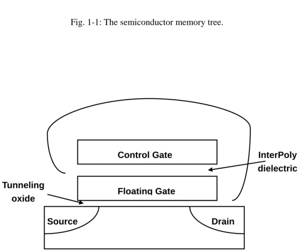
Fig. 1-1: The semiconductor memory tree.
Fig. 1-2: The floating gate (FG) structure. The polysilicon is used as floating gate for data storage.
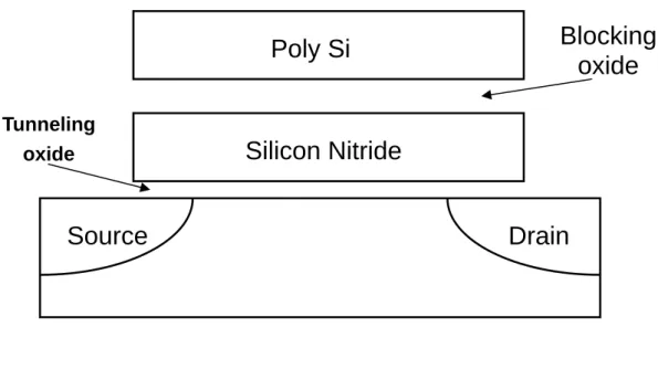
Fig. 1-3: The conventional SONOS memory structure. Silicon nitride is used as charge trapping layer.
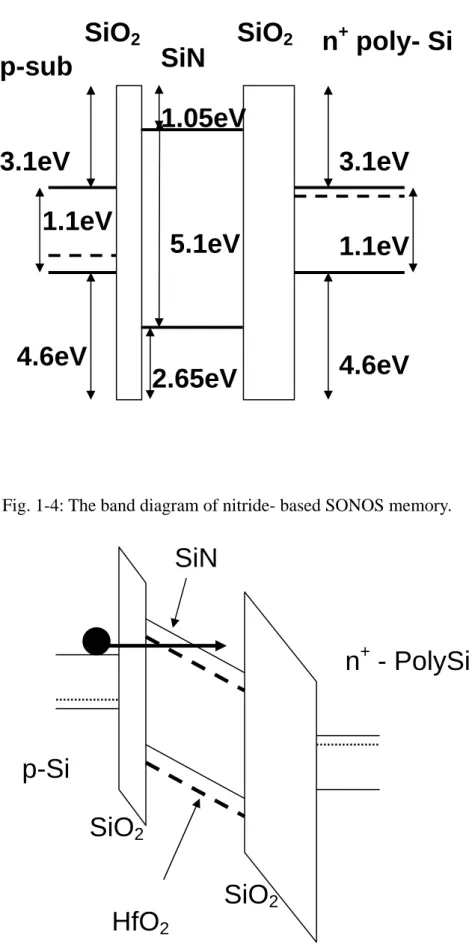
Fig. 1-4: The band diagram of nitride- based SONOS memory.
Fig. 1-5: The band diagram comparison of SONOS-type memory of nitride and HfO2
charge trapping layer when programming (SiN: solid line, HfO2: dash line).
Fig. 1-6: Applications of sol-gel method. Fig. 1-7: Three steps of sol-gel process.
Chapter 2
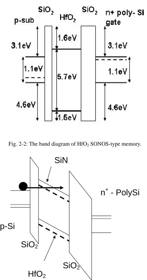
Fig. 2-1: The band diagram of nitride- based SONOS memory. Fig. 2-2: The band diagram of HfO2 SONOS-type memory.
Fig. 2-3: The band diagram comparison of SONOS-type memory of nitride and HfO2
charge trapping layer when programming (SiN: solid line, HfO2: dash line).
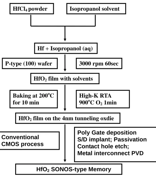
Fig. 2-4: The process flow of the HfO2 SONOS-type memory.
Fig. 2-6: The Id-Vg curve of the device. (Program: Vg=15V, Vd=10V, 10 msec; Erase: Vg= -10V, Vd= 10V, 1sec)
Fig. 2-7: The program speed curve of the sol-gel-derived HfO2 SONOS-type memory.
Fig. 2-8: The erase speed curve of the sol-gel-derived HfO2 SONOS-type memory.
Fig. 2-9: The data retention of the sol-gel-derived HfO2 SONOS-type memory.
Fig. 2-10: The endurance characteristics of the HfO2 SONOS-type memory.
Fig. 2-11: The drain disturbance characteristics of sol-gel HfO2 device.
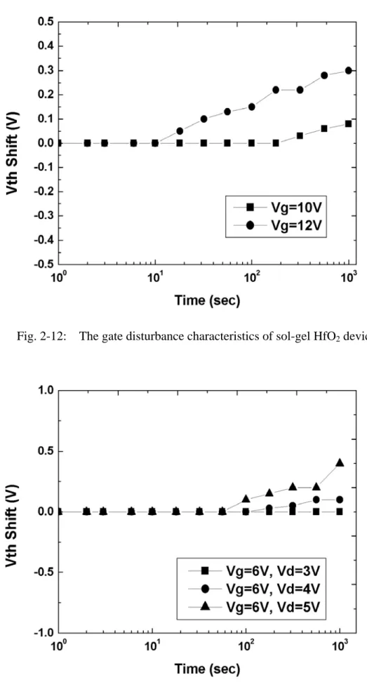
Fig. 2-12: The gate disturbance characteristics of sol-gel HfO2 device.
Fig. 2-13: The read disturbance characteristics of sol-gel HfO2 device
Fig. 2-14: The XPS curve of the sol-gel-derived HfO2 thin film.
Chapter 3
Fig. 3-1: The process flow of the ZrO2 SONOS-type memory.
Fig. 3-2: The structure of the sol-gel ZrO2 SONOS-type memory.
Fig. 3-3: The Id-Vg curve of the device. (Program: Vg=15V, Vd=10V, 10 msec; Erase: Vg= -10V, Vd= 10V, 1sec)
Fig. 3-4: The band diagram of ZrO2 SONOS-type memory.
Fig. 3-5: The program speed of the sol-gel ZrO2 SONOS-type memory.
Fig. 3-7: The charge retention curve of sol-gel ZrO2 SONOS-type memory.
Fig. 3-8: The endurance characteristics of sol-gel ZrO2 SONOS-type memory.
Fig. 3-9: The drain disturbance characteristics of sol-gel ZrO2 device.
Fig. 3-10: The gate disturbance characteristics of sol-gel ZrO2 device.
Fig. 3-11: The read disturbance characteristics of sol-gel ZrO2 device.
Fig. 3-12: The XPS curve of the sol-gel-derived ZrO2 thin film.
Chapter 4
Fig. 4-1: The process flow of the binary high-k SONOS-type memory. Fig. 4-2: The structure of the binary high-k SONOS-type memory.
Fig. 4-3: The Id-Vg curve of the device. (Program: Vg=15V, Vd=10V, 10 msec; Erase: Vg= -10V, Vd= 10V, 1sec)
Fig. 4-4: The program speed of the binary high-kSONOS-type memory. Fig. 4-5: The erase speed of the binary high-kSONOS-type memory.
Fig. 4-6: The program speed comparison of HfO2, ZrO2 and binary high-k memory.
(Vg= 10V, Vd=10V)
Fig. 4-7: The program speed comparison of HfO2, ZrO2 and binary high-k memory.
(Vg= 12V, Vd=10V)
Fig. 4-8: The program speed comparison of HfO2, ZrO2 and binary high-k memory.
(Vg= 15V, Vd=10V)
Fig. 4-10: The endurance characteristics of sol-gel binary high-k SONOS-type memory.
Fig. 4-11: The drain disturbance characteristics of sol-gel binary high-k device. Fig. 4-12: The gate disturbance characteristics of sol-gel binary high-k device. Fig. 4-13: The read disturbance characteristics of sol-gel binary high-k device. Fig. 4-14: The TEM image of the sol-gel-derived binary high-k nanocrystals. Fig. 4-15: The TEM image of the HfZrOx nanocrystals. [6]
Chapter 1
Introduction
1-1 Evolution of Flash Memory
The semiconductor memories based on complementary metal-oxide-semiconductor (CMOS) technology can be divided into two categories as depicted in Fig. 1:
─The volatile memory: this type memory will lose the storage data if the power supply is off, like static random access memory (SRAM) and dynamic random access memory (DRAM).
─The non-volatile memory: this type memory will keep the storage data even if the power supply is off, like electrically programmable read only memory (EPROM), electrically erasable programmable read only memory (EEPROM), and the flash memory.
The most explosive growth field of the semiconductor memory is the Flash memory. The advantages of Flash memory are that it can be electrically written more than 100K times with byte programming and sector erasing and with the smallest cell size (one transistor cell) [1]-[2]. The Flash memory cell is used floating gate (FG) structure as illustrated in Fig. 2.
The first floating gate nonvolatile semiconductor memory was invented by S. M. Sze and D. Kahng in 1967 [3]. The conventional FG memory (in Fig. 2) used polysilicon as a charge storage layer surrounded by the dielectric [1]. The FG structure can achieve high densities, good program/erase speed and good reliability
for Flash memory application. However, the FG memory concerns the scaling issue [4]. When the tunneling oxide thickness is below 10nm, the storage charge in the polysilicon is easy to leak due to a defect in the tunneling oxide formed by repeated write/erase cycles or direct tunneling current.
In order to solve the scaling issue of FG memory, the polySi-Oxide-Nitride-Oxdie-Silicon (SONOS) memory has been studied recently [4]. SONOS memory has better charge retention than floating gate memory when floating gate bitcell’s tunneling oxide is below 10nm due to its spatially isolated deep-level traps. Hence, a single defect in the tunneling oxide will not cause the discharge of the memory cell [4]. The structure of SONOS memory is depicted in Fig. 3. The SONOS memory uses silicon nitride as charge trapping layer, and the band diagram is depicted in Fig.4. The conduction band offset between silicon substrate and nitride is 2.05eV. When we apply a positive voltage on the gate, the band will bend downward as illustrated in Fig. 4 [5]. The electrons in the Si-sub conduction band will tunnel through the tunneling oxide and a portion of nitride to be trapped in the charge trapping layer. Before electrons are trapped in the nitride, they must tunnel a portion of nitride and this will degrade the program speed. Besides this, the conduction band offset between nitride and tunneling oxide is only 1.05eV and the trapped electron back tunneling may also occur. To solve these problems, the high-k materials are the possible candidates to replace the traditional silicon nitride as the charge trapping layer.
The advantages of high-k material are smaller barrier height between silicon substrate and high-k charge trapping layer and more trapping sites than silicon nitride. The smaller barrier height can get faster program speed under the same stress condition. More trapping sites can achieve larger Vth shift for larger memory window. For HfO2 high-k material in Fig. 5, the conduction band offset between silicon
substrate and HfO2 is 1.5eV. When FN programming, the electron will tunnel shorter
distance in HfO2 than in nitride to be trapped. This can achieve high program/erase
speed. Thus, it is beneficial to use a high-k material as the charge trapping layer in a SONOS-type memory device, provided that there are many deep level trapping sites in the high-k material. The electron trap level of ZrO2 is 1.0eV [6] and 1.5eV of JVD
HfO2 [7], and this is deeper than 0.8eV of nitride. It is desirable to choose a high-k
material with small barrier height with silicon substrate and deep trapping level as charge trapping layer to achieve high program/erase speed and good reliability due to deep trapping level. High-k material has large dielectric constant, a wide band gap, good, high trap site density and is also suitable for SONOS-type memory application.
1-2 Motivation
1-2.1 The Deposition Method of High-k Material
The deposition method of high-k material must satisfy two requirements: first, to achieve good quality of deposited film for the applications, particularly with respect to the interface controllability, and second, to be compatible with the conventional CMOS processes. To date, the technologies applied on high-k film deposition includes: physical vapor deposition (PVD), metal organic chemical vapor deposition (MOCVD), atomic layer deposition (ALD).
The PVD process needs a high-k metal target for sputtering under oxygen ambient to form high-k oxide film. MOCVD is a material synthesis process using a variety of solid or gaseous precursors in which the precursors will thermally decompose into reactive species on the substrate surface and combine to form a thin film. In MOCVD process, a high substrate temperature is necessary to get better film
quality and reduce impurity concentration. However, MOCVD process faces a challenging task: how to make the concentration of impurity like carbon in the film as low as possible [8]. ALD process can control film growth in a layer-by-layer formation at atomic scale. The main problem of ALD process is that: the very limited selections of available precursor sources remaining precursor induce chlorine contamination in the films. Besides this, in the special case of metal electrode deposition, precursor sources for ALD process are still not available [9]-[10].
1-2.2 The Sol-Gel Spin Coating Method
A sol is a colloidal suspension of solid particles about 0.1~1 μm in a liquid phase [11]. A gel is a solid material network containing a liquid component [12]. The sol-gel spin coating process includes four steps: First, the desired colloidal particles dissolved in a solvent to form a sol. Secondly, the deposition of sol solution produces the coatings on the substrates by spraying, dipping or spinning. Thirdly, the particles in sol are polymerized through the removal of the stabilizing components and produce a gel in a state of a continuous network. Finally, the final heat treatments pyrolyze the remaining organic or inorganic components and form an amorphous or crystalline coating [13]-[16].
Sol-gel method has been applied to the fabrication of the organic and inorganic hybrid materials for specific applications. Liquid phase processing enables the molecular scale mixing of precursors, leading to homogeneous, multi-component materials. The most interesting feature of sol-gel processing is its capability to synthesize a new type of materials called inorganic-organic hybrids. In addition, metal oxides with various shapes, such as thin films, porous structures, and particles, can also be formed by sol-gel method, thus increasing the applicability to many specific usages [17]-[19].
Sol-gel spin coating method is used more and more widely in the creation of ceramic fibers, thin films, and aerogel, because it allows the fabrication of very homogeneous and very thin fibers and films. Figure 6 illustrates the process and products of the sol-gel method [20]. These sol-gel ceramic fibers are mostly used in the optical industry as fiber optic cores. For the sol-gel method applied on the thin film deposition, dense film can be made by coating a substrate material with the sol and letting it gel. This leaves a very dense film on the substrate which can have a number of the uses such as catalysts, molecular sieves, chemical sensing, optical devices, and nanoelectronic devices [21]. Aerogels are a class of ceramic materials fabricated from a sol-gel by carefully evacuating the solvent to leave a fragile polymer or oxide network which is 90 ~99% air by volume. Silica aerogels have interesting applications, among them as thermal insulation materials [22].
1-2.3 Motivation
The sol-gel spin coating method using metal halides hydrolyzed in organic or colloidal solvents to form precursor compound and undergo hydrolysis, condensation, and polymerization steps to form metal oxide networks as shown in Fig. 7. The advantages of using sol-gel method to fabricate high-k film are its cheaper precursor and low cost tool than ALD, PVD, and MOCVD, and its ability to synthesize various types of thin films. To the best our knowledge, the sol-gel spin coating high-k film has not been reported as a charge trapping layer for Flash memory. In this thesis, the high-k charge trapping layer of SONOS-type memory deposited by sol-gel spin coating method is proposed. We fabricated three SONOS-type memories with three different high-k charge trapping layer using different precursors. The two of the three different high-k charge trapping layers are HfO2 and ZrO2 using HfCl4 and ZrCl4 as
spin coating method is its capability to synthesize a new type of materials. So we combined the precursors of two different high-k material, i.e. HfCl4 and ZrCl4, to get a
new type high-k material. After sol-gel spin coating, we used high-k rapid thermal annealing (RTA) at 900oC 1min in O2 ambient to form high-k dielectric film. The
device performance like Id-Vg, data retention, endurance, program / erase speed and disturbance test is measured to examine the quality of the high-k charge trapping layer deposited by sol-gel method. From those data, the sol-gel spin coating is demonstrated to be applicable to the high-k dielectrics deposition.
1-3 Thesis Organization
This thesis includes five chapters. In this thesis, we study the device performance of the SONOS-type memory using high-k dielectrics as charge trapping layer deposited by sol-gel spin coating method.
In Chapter 1, we introduce the background of the Flash memory and explain why SONOS-type memory with high-k charge trapping layer is studied to replace the traditional floating gate memory. The sol-gel spin coating method and motivation of this thesis are also mentioned in this chapter.
In Chapter 2, we introduce our experiment to fabricate SONOS-type memory with HfO2 charge trapping layer using sol-gel spin coating method. After solution
coating, we use RTA treatment to form HfO2 film. The sol-gel-derived film thickness
is about 10nm by ellipsometer measurement. X-ray photoelectron spectrometer (XPS) is done to analyze the composition of the sol-gel-derived film. The electrical characteristics like Id-Vg curve, program/erase speed, data retention, and endurance are measured to know the device performance.
In Chapter 3, the ZrO2 charge trapping layer SONOS-type memory is fabricated.
We also do physical analysis and electrical measurement to examine the sol-gel-derived thin film quality.
In Chapter 4, we use sol-gel method to combine two high-k precursors of HfO2
and ZrO2 and to deposit thin film consist of two high-k material as a charge trapping
layer for SONOS-type memory. Transmission electron microscopy (TEM) is done to study the physical characteristics of the binary high-k thin film. Besides the physical analysis, the electrical characteristics of device are measured.
Fig. 1-1: The semiconductor memory tree.
Fig. 1-2: The floating gate (FG) structure. The polysilicon is used as floating gate for data storage.
Tunneling oxide
Control Gate InterPoly
dielectric Floating Gate
Poly Si
Silicon Nitride
Tunneling oxideBlocking
oxide
Source Drain
Fig. 1-3: The conventional SONOS memory structure. Silicon nitride is used as charge trapping layer.
SiO
2SiO
2n
+poly- Si
SiN
Fig. 1-4: The band diagram of nitride- based SONOS memory.
Fig. 1-5: The band diagram comparison of SONOS-type memory of nitride and HfO2 2
charge trapping layer when programming (SiN: solid line, HfO : dash line).
SiO
SiO
p-Si
n
+- PolySi
2HfO
2p-sub
1.05eV
23.1eV
1.1eV
4.6eV
3.1eV
5.1eV
1.1eV
4.6eV
2.65eV
SiN
Fig. 1-6: Applications of sol-gel method.
1-4 Reference
Proc. of the IEEE, 91, 489
. Pavan, R. Bez, P. Olivo, and E. Zanoni, Proc. of the IEEE, 85, 1248(1997).
e, “Physics of Semiconductor Devices, 2nd Edition”, John Wiley & Sons.
lvo, C. Gerardi, R. V. Schaijk, S. A. Lombardo, D. Corso, C. Plantamura,
Y.-N. Tan, W.-K. Chim, B. J. Cho, and W.-K. Choi, IEEE Trans. Electron
maguchi, H. Satake, and N. Fukushima, IEEE Trans. Electron Devices, 51,
agawa, Y. Di, J. Kim, R. Carruthers, M. Gibson, T.
acher, and J. Lindner,
/issues/newsletter_i1_03/pdf/avd.pdf
[1]. R. Bez, E. Camerlenghi, A. Modelli, and A. Visconti, (2003).
[2]. P
[3]. S.M. Sz
[4]. B. D. Sa
T. Serafino, G. Ammendola, M. V. Duuren, P. Goarin, W. Y. Mei, K. V. D. Jeugd, H. Baron, M. Gély, P. Mur, and S. Deleonibus, IEEE Trans. Device and
Materials Reliability, 4, 377 (2004).
[5].
Devices, 51, 1143 (2004).
[6]. T. Ya 774 (2004).
[7]. W. Zhu, T.P. Ma, T. Tam Furukawa, IEDM, 463 (2001).
[8]. M. Schum
[9]. S. Haukka, E. L. Lakomaa, and T. Suntola, in Adsorption and Its Applications in
Industry and Environmental Protection: Stud. Surf. Sci. Catal., ed. A. Dabrowski,
Vol.120, Elsevier, Amsterdam 1998, pp. 715-750.
[10]. S. Ek, Helsinki University of Technology Inorganic Chemistry Publication Series, No.4, Espoo 2004.
[11]. C. J. Brinker, and G. W. Scherer, Sol-gel science: The Physics and Chemistry of
Sol-Gel Processing, San Diego, CA, Academic Press Inc., pp.2.10, 1990.
[12]. C. W. Turner, Sol-Gel Process-Principles and Applications, Ceramic
Bulletin,vol.70, pp. 1487-1490, 1991.
[13]. C. J. Brinker and G. W. Sherer, Academic Press, San Diego, 1990.
[14]. C. J. Brinker, A. J. Hurd, P. R. Schunk, C. S. Ashley, R. A. Cairncross, J. Samuel, K. S. Chen, C. Scotto, and R. A. Schwartz , Metallurgical and Ceramic Protective
Coatings, Chapman & Hall, London, 1996, pp. 112-151.
[15]. T. Troczynski and Q. Yang, U. S. Pat., May, 2001.
[16]. T. Olding, M. Sayer, and D. Barrow, Thin Solid Films, 581(2001).
[17]. T. Kololuoma, S. M. Nissila, and J. T. Rantala, Sol-Gel Optics V. Society of
[18]. C. J. Brinker, A. J. Hurd, P. R. Schunk, G. C. Frye, and C. S. Ashley, Non-Cryst.
Solids. 147,424 (1992).
[19]. C. J. Brinker, D. M. Smith, R. Deshpande, P. M. Davis, S. Hietala, G. C. Frye, C. S. Ashley, and R. A. Assink, Catal. Today, 14, 155, (1992).
[20]. Sol-Gel Technology, http://www.chemat.com/html/solgel.html
[21]. M. Marvola, J. Kiesvaara, K. Jarvinen, M. Linden, and A. Urtti, Sol-Gel Derived
Silica Gel Monoliths And Microparticles As Delivery in Tissue Admonistration,
Division of Biopharmaceutics and Pharmacokinetics Department of Pharmacy University of Helsinki (2001).
Chapter 2
SONOS-Type Flash Memory with HfO
2as
Charge Trapping Layer Using HfCl
4as
Precursor
2-1 Introduction
The traditional SONOS (PolySi-Oxide-Nitride-Oxide-Si) flash memory uses silicon nitride as charge trapping layer. The silicon nitride has 5.1eV band gap, 2.05eV barrier height with silicon, dielectric constant of 7.5, and the trapping level is 0.8eV below the nitride conduction band [1, 2]. The SONOS memory has better data retention than floating gate memory due to its spatially isolated trapping site when tunneling oxide is below 10nm. But traditional SONOS memory still faces some challenging task. One is the program speed. The conduction band offset between nitride and tunneling oxide is 1.05eV and the barrier height between silicon nitride and silicon substrate is 2.05eV as illustrated in Fig. 1 [3]. Figure 2 illustrates the band diagram of HfO2 SONOS-type memory. When we apply a positive gate voltage where
modified Fowler–Nordheim (F–N) tunneling dominates, the electrons in the silicon substrate need to tunnel a long portion of silicon nitride to be trapped in the charge trapping layer due to the large barrier height between silicon nitride and silicon substrate. Fig. 3 depicts the comparison of silicon nitride and HfO2 [3]. Another task
of silicon nitride is that its conduction band offset between nitride and tunneling oxide is 1.05eV. The trapped electrons are easily thermally de-trapped in this shallow trapping well resulted into data retention loss. So a small barrier height with silicon and large conduction band offset with silicon oxide material is needed to achieve high
program speed and good charge retention characteristics.
HfO2 has dielectric constant of 25, band gap 5.7eV, 1.5eV barrier height with
silicon, and the trapping level is 1.5eV for JVD HfO2 [4, 5]. HfO2 has smaller barrier
height with silicon substrate and larger conduction band offset with tunneling oxide than nitride. So it is suitable for SONOS-type charge trapping layer application.
In this chapter, we fabricate theSONOS-type memory using an HfO2 as charge
trapping layer deposited by a very simple sol-gel spin coating method and 900oC 1 min rapid thermal annealing (RTA). We examine the quality of sol-gel HfO2 charge
trapping layer by XPS, Id-Vg, charge retention, and endurance.
2-2 Experimental
HfCl4 (99.5%, Aldrich, USA) was used as the precursor for the synthesis of
hafnia. A mother sol solution was first prepared by dissolving HfCl4 in isopropanol
(IPA; Fluka; water content < 0.1%) under vigorous stirring in an ice bath. The sol solution was obtained by fully hydrolyzing HfCl4 with a stoichiometric quantity of
water in IPA to yield a Hf:IPA molar ratio of 1:1000.
The fabrication of a sol-gel spin coating HfO2 SONOS-type memory is started
with LOCOS isolation process on p-type (100) 150-mm silicon substrate. At the beginning, a 4-nm tunneling oxide was thermally grown at 925oC by furnace oxidation. The solution of Hf:IPA molar ratio of 1:1000 is coated by spin coater at 3000rpm for 60 sec at ambient temperature (25oC). The as-deposited thin film was initially baked at 200oC for 10min to densification and followed by 1min high-k rapid thermal annealing (RTA) in O2 ambient to form the HfO2 charge trapping layer. The
film thickness was 10nm measured by ellipsometer. The 30nm-thick blocking oxide was deposited by high density plasma enhanced chemical vapor deposition
(HDPCVD) followed by poly-Si gate 200nm deposition. After gate deposition, the following processes are gate pattering, the source/drain implant (S/D) of the dosage of Phosphorus 5E15 20KeV, S/D activation with 900oC RTA in N2 ambient for 30 sec,
CVD passivation oxide and the rest of the subsequent MOS processes were used to fabricate this HfO2 SONOS-type memory. The process flow and the structure of the
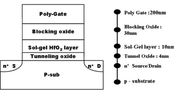
HfO2 SONOS-type memory are depicted in Fig. 4 and Fig. 5 respectively.
2-3 Results and Discussion
In this section, the physical and electrical characteristics of sol-gel-derived HfO2 SONOS-type memory were discussed.
2-3.1 Electrical Characteristics
2-3.1.1 Id-Vg Curve
Figure 6 shows the Id-Vg curve of the device under program and erase operations. We use channel hot electron injection (CHEI) to program and band to band hot hole to erase (BTBHH). The program condition is Vg= 15V, Vd= 10V with 10 msec stress. The erase condition is Vg= -10V, Vd= 10V with 1 sec stress. The Vth after programming becomes to 7.92V from 4.3V of the original fresh state. After erasing, the Vth shifts leftward to 4.95V. The memory window is about 3V. We think the Vth shift rightward is due to electron trapping in the HfO2 layer. The band offset is
the reason why trapping occurred. Fig. 2 is the typical band diagram for the HfO2
SONOS-type memory. The energy barrier of electrons is 3.1eV between tunneling oxide and p-Si substrate. During programming, the electrons in the substrate gain energy from the applied voltage Vg and Vd. If the energy is enough to cross the 3.1eV energy barrier, the hot electrons will inject to the HfO2 charge trapping layer and be
trapped. This causes the Vth change. The energy barrier of holes is 4.6eV between tunneling oxide and p-Si substrate. When erasing, we apply a negative gate voltage and positive drain voltage to generate hot hole in the substrate. If the hot hole in the substrate achieves enough energy to cross the 4.6eV energy barrier, it can reach the HfO2 charge trapping layer and cause the Id-Vg curve shift toward left.
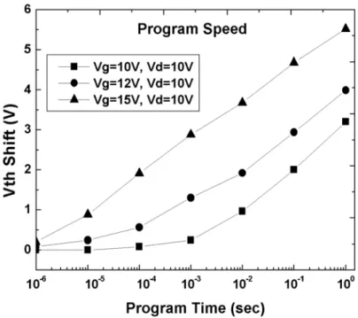
2-3.1.2 Program/Erase Speed
The program speed is shown in Fig. 7.We show three different stress conditions: Vg=10V, 12V, 15V; Vd=10V. As Fig. 7 shows, the condition Vg=12V, Vd=10V, 1 msec cause Vth shift 1.2V. With the Vg increasing, the Vth shift also increases and the program speed is faster. Figure 8 shows the normalized erase speed of the device for three different conditions: Vg= -10V, -12V, and –15V with the same Vd=10V. We can see as the gate voltage becomes more negative, the Vth shift more. This is because as the gate voltage become more positive for programming or more negative for erasing, more hot electrons or hot holes are generated. So more and more hot electrons or hot holes can be trapped in the charge trapping layer. Hence, the Vth shift increases as gate voltage increases.
2-3.1.3 Data Retention Characteristics
Fig. 9 is the data retention characteristics of HfO2 SONOS-type memory
measured at 25oC and 85oC. We find the small charge loss with time in the sol-gel SONOS memory. The curve shows only 6% charge loss as measure time up to 104 sec at 25oC and the charge loss at 85oC is 20%. We infer the small charge loss at room temperature is from the electron deep trap of sol-gel HfO2 charge trapping layer.
2-3.1.4 Endurance Characteristics
The endurance of the sol-gel HfO2 SONOS memory is shown in Fig. 10. The
measure condition is - program: Vg = 15V, Vd = 10V, 1 msec; erase: Vg = -10V, Vd = 10V, 10 msec. A very small increase of the erase Vth is observed from the figure. This is due to the distribution profile misalignment of programmed electron and erased holes. So some electrons are left in the charge trapping layer resulted into erased state Vth increasing. In addition, no significant window narrowing is observed. After 105 P/E cycles, the memory window is still fixed around 2.8V. This finding suggests the simple sol-gel process can be incorporated into the SONOS memory fabrication.
2-3.1.5 Disturbance Measurement
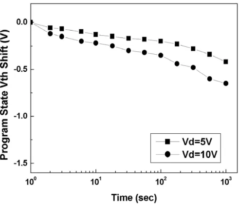
Figure 11 shows drain disturbance measurement of the sol-gel HfO2 device. We
applied two stress conditions: Vd=5V and Vd=10V with Vg=Vs=Vb=0V to the device. We can see from the Fig. 11 after 1000 sec stress the programmed state Vth loss is 0.42V for Vd=5V and 0.65V for Vd=10V.
Figure 12 shows the gate disturbance measurement of the device for two stress conditions: Vg= 10V and Vg=12V with Vd=Vs=Vb=0V. The applied gate voltage will attract electrons in the substrate tunneling to the HfO2 layer by FN tunneling
mechanism and result into Vth increase. After 1000 sec stress, the fresh state Vth increases 0.08V and 0.3V for the Vg= 10V and Vg=12V, respectively.
Figure 13 shows the read disturbance measurement of the device. The measurement conditions are fixed Vg=6V with different Vd= 3V, 4V, and 5V for 1000 sec stress. The stress caused the fresh state Vth increase 0V, 0.1V, and 0.4V for Vd= 3V, 4V, and 5V conditions, respectively. The fresh state Vth increases as the drain voltage increases. We think this is because as the drain voltage increases, more hot
charge trapping layer resulted to Vth increases.
2-3.2 Physical Characteristics
In order to analyze the chemical composition of hafnia film, elements are detected by X-ray photoemission spectroscopy (XPS). Fig. 14 demonstrates the high-resolution spectrum of Hf 4f peak for the film. The Hf 4f7/2 peak was
approximately 16.8 eV with a difference of 1.7 eV in binding energy between the Hf 4f5/2 and Hf 4f7/2 peaks at RTA treatment temperature 900°C. This observation
suggests the sol-gel film is HfO2 and is similar with the literature identification for
ALD HfO2.
From the Hf 4f spectrum, we observed clearly RTA annealing at 900°C in O2
treatment led to remarkable changes in the XPS spectra. This change, which is apparent from the increase in the signal of the Hf–O bonds upon increasing the annealing temperature. The as-deposited hafnia film is mainly HfO2-δ (δ>0), while the
annealing under oxygen ambient can decrease the δ value. This finding indicates that structural composition of the HfO2 has occurred.
2-4 Summary
In this chapter, we propose a new spin coating method to deposit charge trapping layer of SONOS memory. We have shown the electric curves, like Id-Vg, charge retention, and endurance, that can demonstrate the quality of sol-gel spin coating high-k layer with some good characteristics in terms of ~ 3V memory window, long charge retention time due to deep trap level in the HfO2 layer, and good endurance up
SiO
2SiO
2SiN
Fig. 2-1: The band diagram of nitride- based SONOS memory.
3.1eV
1.1eV
4.6eV
3.1eV
1.1eV
4.6eV
1.05eV
n
+poly- Si
p-sub
5.1eV
2.65eV
Fig. 2-2: The band diagram of HfO2 SONOS-type memory.
SiN
n
+- PolySi
p-Si
SiO
2SiO
2HfO
2Fig. 2-3: The band diagram comparison of SONOS-type memory of nitride and HfO2
HfCl
4powder
Isopropanol solvent
Hf + Isopropanol (aq)
P-type (100) wafer
3000 rpm 60sec
HfO
2film with solvents
Baking at 200
oC
for 10 min
High-K RTA
900
oC O
21min
HfO
2film on the 4nm tunneling oxdie
Fig. 2-4: The process flow of the HfO2 SONOS-type memory.
Poly Gate deposition
Conventional
CMOS process
S/D implant; Passivation
Contact hole etch;
Metal interconnect PVD
Fig. 2-6: The Id-Vg curve of the device.
Fig. 2-7: The program speed curve of the sol-gel-derived HfO2 SONOS-type memory.
2-5 Reference
[1]. H. Aozasa, I. Fujiwara, A. Nakamura, and Y. Komatsu, “Analysis of Carrier Traps in Si3N4 in Oxide/Nitride/Oxide for Metal/ Oxide/Nitride/Oxide Silicon Nonvolatile Memory”, Japanese Journal of Applied Physics, Vol.38, part 1, No. 3A, pp.1441-1447, 1999.
[2]. Y. Yang, and M. H. White, “Charge retention of scaled SONOS nonvolatile memory devices at elevated temperatures”, Solid State Electronics, Vol. 44, pp.949-958, 2000.
[3]. Y.N. Tan, W.K. Chim, B.J. Cho, and W.K. Choi, “Over-erase phenomenon in SONOS-type flash memory and its minimization using a hafnium oxide charge storage layer,” IEEE Trans. Electron Devices, vol. 51, pp. 1143-1147, July 2004.
[4]. G. D. Wilk, R. M. Wallace, and J. M. Anthony, “High-k gate dielectrics: Current status and materials properties considerations”, Journal of Applied Physics, Vol. 89, pp. 5243-5275, 2001.
[5]. W. Zhu, T.P. Ma, T. Tamagawa, Y. Di, J. Kim, R. Carruthers, M. Gibson, and T. Furukawa, “HfO2 and HfAlO for CMOS : Thermal stability and current transport,” in
Chapter 3
SONOS-Type Flash Memory with ZrO
2as
Charge Trapping Layer Using ZrCl
4as
Precursor
3-1 Introduction
ZrO2 has a dielectric constant of about 25, wide band gap of 5.7eV, good thermal
stability, high hardness, high ionic conductivity, high melting point, chemical hardness, and high refractive index [1, 2]. Typically, ZrO2 is an excellent heat-resistant
and chemically durable material that is used, for example, as a material for furnaces [3].
ZrO2 is also a potential dielectric candidate to replace SiO2 as gate dielectric due
to its large barrier height with silicon substrate [4] and thermal stability with silicon [5,6]. The conduction band offset between ZrO2 and Si is 1.5eV and 3.1eV for valence
band offset. The large band offsets means the barrier height for both electrons and holes are high. ZrO2 is not only a gate dielectric but also a charge trapping layer for
SONOS memory application due to its high trapping site density and its deep trapping level of 1.0eV.
In You et al. [7], he fabricated a ZrO2 capacitor on silicon substrate using sol-gel
spin coating method with good characteristics. The electrical properties such as breakdown field is 12.5 MV/cm and gate current density is less than 10-7 A/cm2 of sol-gel formed ZrO2 ultrathin films with 900oC annealing displayed good electrical
insulation. In his paper, he demonstrated the sol-gel-derived ZrO2 thin films are
In this chapter, we fabricated a ZrO2-based SONOS-type memory using sol-gel
spin coating method. Physical and electrical analysis like XPS, Id-Vg, retention, and program/erase speed are measured to evaluate the performance of sol-gel ZrO2 film to
use as a charge trapping layer for SONOS-type memory application.
3-2 Experimental
ZrCl4 (99.5%, Aldrich, USA) was used as the precursor for the synthesis of
zirconia. A mother sol solution was first prepared by dissolving ZrCl4 in isopropanol
(IPA; Fluka; water content < 0.1%) under vigorous stirring in an ice bath. The sol solution was obtained by fully hydrolyzing ZrCl4 with a stoichiometric quantity of
water in IPA to yield a Zr:IPA molar ratio of 1:1000.
The fabrication of a sol-gel spin coating ZrO2 SONOS-type memory is started
with LOCOS isolation process on p-type (100) 150-mm silicon substrate. At the beginning, a 4-nm tunneling oxide was thermally grown at 925oC by furnace oxidation. The solution of Zr:IPA molar ratio of 1:1000 is coated by spin coater at 3000rpm for 60 sec at ambient temperature (25oC). The as-deposited thin film was initially baked at 200oC for 10min to densification and followed by 1min high-k rapid thermal annealing (RTA) at 900oC in O2 ambient to form the ZrO2 charge trapping
layer. The film thickness was 10nm measured by ellipsometer. The 30nm-thick blocking oxide was deposited by high density plasma enhanced chemical vapor deposition (HDPCVD) followed by poly-Si gate 200nm deposition. After gate deposition, the following processes are gate pattering, the source/drain implant (S/D) of the dosage of Phosphorus 5E15 20KeV, S/D activation at 900oC RTA in N2
processes were used to fabricate this ZrO2 SONOS-type memory. The process flow
and the structure of the ZrO2 as a charge trapping layer in this high-k SONOS-type
Flash memory are depicted in Fig. 1 and Fig. 2, respectively.
3-3 Results and Discussion
In this section, the physical and electrical characteristics of sol-gel-derived ZrO2 SONOS-type memory were discussed.
3-3.1 Electrical Characteristics
3-3.1.1 Id-Vg Curve
Figure 3 shows the Id-Vg curve of ZrO2 SONOS-type memory. We use channel
hot electron injection (CHEI) to program and band to band hot hole to erase
(BTBHH). It is observed that after the Vg= 15V, Vd= 10V, 10 msec programming, the threshold voltage (Vth) shift from 3.75V of the fresh state to 7.35V due to electron
trapping. After Vg= -10V, Vd= 10V, 1 sec erasing, the Vth shifts leftward to 4.35V. The memory window is 3V and this satisfies the requirement of the typical memory device – i.e. the memory window is larger than 0.7V. The electron trapping can be explained by the band diagram proposed in Fig. 4. This figure indicates the energy barrier between tunneling oxide and Si-sub is 3.1eV. When the electrons in the conduction band of silicon substrate gain enough energy from the applied voltage to across over the barrier, they can across the tunneling oxide and be trapped in the ZrO2
layer. The electron trapping causes the Id-Vg curve (in Fig. 3) after programming moving rightward and the Vth increases. Another points observed from the Id-Vg curve are that the subthreshold slope degradation of erased cell and the erased curve can’t match with the original fresh curve. The subthreshold slope degradation of
erased cell is because the BTBHH injection may damage the bottom oxide [8, 9]. There are two possible reasons why the erased curve can’t match with the original fresh curve. One is that the distribution of trapped electrons programmed by CHEI does not match with the hole by BTBHH so the injected holes during erase may not completely annihilate all of the trapped electrons leading to some negative charge left in the ZrO2 layer to result in the Vth slight increasing [9, 10]. The other reason is
because that some electrons are trapped in the deep trap level of ZrO2 and hard to
escape from the trapping site. This is beneficial for the memory device to retention.
3-3.1.2 Program/Erase Speed
Figure 5 shows the program speed of the ZrO2 SONOS-type memory. Figure 5
shows the program characteristics for three different stress conditions: Vg=10V, 12V, 15V and Vd=10V. The mechanism is also CHEI. The condition Vg=15V, Vd=10V, 0.1ms causes Vth shift about 2V. We can see from the figure as the applied gate voltage increases, the Vth shift also increases. This is because the larger gate voltage is applied, the more “hot” electrons are generated. There are more electrons able to cross the barrier height and trapped in the ZrO2 layer, so the Vth shift increases. The
normalized erase speed curve is appeared in Fig. 6, and the same explanation can be applied on Vth shift as gate voltage becomes more negative. Using CHEI to program and BTBHH to erase can get high program/erase efficiency.
3-3.1.3 Data Retention Characteristics
The retention characteristics of ZrO2 SONOS-type memory is depicted in Fig. 7.
The retention measurement is at two temperatures of 25oC and 85oC. We find the small charge loss with time in the sol-gel ZrO2 SONOS-type memory only 5% charge
contribution is from the electron deep trap of sol-gel ZrO2 charge trapping layer. The
small amount charge loss at room ambient may be due to the direct tunneling current from the ZrO2 charge trapping layer to the Si-substrate or oxide trap-assisted
tunneling due to the defect in the tunneling oxide.
3-3.1.4 Endurance Characteristics
Figure 8 shows the endurance of the sol-gel ZrO2 SONOS-type memory. The
measure condition is program: Vg = 15V, Vd = 10V, 1 msec; erase: Vg = -10V, Vd = 10V, 10 msec. As we can see from the figure, the memory window is 2.7V. A very small increase of the erase Vth is observed. In addition, no significant window narrowing is appeared. This is due to the formation of deep trap level that makes it hard to erase all trapped electrons or misalignment of the CHEI and BTBHH distribution profile in the ZrO2 layer. After 105 P/E cycles, the memory window is still
larger than 0.7 V. This finding suggests the simple sol-gel process to deposit a ZrO2
charge trapping layer can be incorporated into the SONOS-type memory fabrication.
3-3.1.5 Disturbance Measurement
Figure 9 shows drain disturbance measurement of the sol-gel ZrO2 device. We
applied two stress conditions: Vd=5V and Vd=10V with Vg=Vs=Vb=0V to the device. We can see from the Fig. 9 after 1000 sec stress the programmed state Vth loss is 0.45V for Vd=5V and 0.68V for Vd=10V.
Figure 10 shows the gate disturbance measurement of the device for two stress conditions: Vg= 10V and Vg=12V with Vd=Vs=Vb=0V. After 1000 sec stress, the fresh state Vth increases 0.1 V and 0.32V for the Vg= 10V and Vg=12V, respectively. Figure 11 shows the read disturbance measurement of the device. The measurement conditions are fixed Vg=6V with different Vd= 3V, 4V, and 5V for 1000
sec stress. The stress caused the fresh state Vth increases 0V, 0.15V, and 0.43V for Vd= 3V, 4V, and 5V conditions respectively. We think as drain voltage increases, the more hot electrons generate and can across the energy barrier to be trapped in ZrO2
layer. This is why fresh state Vth increases.
3-3.2 Physical Characteristics
In order to analyze the chemical composition of the film, elements are detected by X-ray photoemission spectroscopy (XPS). Figure 11 demonstrates the high-resolution spectrum of Zr 3d peak for the film. From the Zr 3d spectrum of the RTA samples, the two typical peaks of Zr 3d5/2 (183.2eV) and Zr 3d3/2 (185.6eV)
from ZrO2 thin film can be observed clearly. This observation suggests that a
complete structural composition of ZrO2 has occurred [7].
3-4 Summary
In this chapter, we fabricate the high-k SONOS-type memory using ZrO2 as the
charge trapping layer deposited by sol-gel spin coating method using ZrCl4 as
precursor and rapid thermal annealing. We have demonstrated the formation of ZrO2
thin film as the charge trapping layer after XPS measurement. The Id-Vg curve and P/E speed curve are measured to demonstrate the memory performance. The data retention at 25oC is 5% loss after 104 sec due to deep trap level in the ZrO2 and good
endurance up to 105 P/E cycles without memory window narrowing. The sol-gel spin coating method is suitable for SONOS-type high-k charge trapping layer deposition.
ZrCl
4powder
Isopropanol solvent
Zr + Isopropanol (aq)
P-type (100) wafer
3000 rpm 60sec
ZrO
2film with solvents
Baking at 200
oC
for 10 min
High-K RTA
900
oC O
21min
ZrO
2film on the 4nm tunneling oxdie
Fig. 3-1: The process flow of the ZrO2 SONOS-type memory.
Poly Gate deposition
Conventional
CMOS process
S/D implant; Passivation
Contact hole etch;
Metal interconnect PVD
Fig. 3-3: The Id-Vg curve of the device.
(Program: Vg=15V, Vd=10V, 10 msec; Erase: Vg= -10V, Vd= 10V, 1sec)
Fig. 3-5: The program speed of the sol-gel ZrO2 SONOS-type memory.
Fig. 3-7: The charge retention curve of sol-gel ZrO2 SONOS-type memory.
Fig. 3-9: The drain disturbance characteristics of sol-gel ZrO2 device.
Fig. 3-11: The read disturbance characteristics of sol-gel ZrO2 device.
3-5 Reference
[1]. S. Ventkataraj, O. Kappertz, C. Liesch, R. Detemple, R. Jayavel, M. Wutting,
Vacuum, 75, 7 (2004).
[2]. W. Zhao, B. K. Tay, G. Q. Yu, S. P. Lau, J. Phys. –Condens. Mat., 15, 7707 (2003).
[3]. A. J. Moulson and J. M. Herbert, Electroceramics, Wiley, NJ (2003).
[4]. W. Zhu, T.P. Ma, T. Tamagawa, Y. Di, J. Kim, R. Carruthers, M. Gibson, T. Furukawa, IEDM, 463 (2001).
[5]. M. Balog, M. Schieber, M. Michman, and S. Patai, Thin Solid films, 47, 190 (1997).
[6]. M. Balog, and M. Schieber, J. Electrochem. Soc., 126,1203 (1979).
[7]. H.C. You, F.H. Ko, and T.F. Lei, “Physical characterization and electrical properties of sol-gel-derived zirconia films,” accepted for J. Electrochem. Soc.
[8]. W.J. Tsai, N.K. Zous, C.J. Liu, C.H. Chen, Tahui Wang, Sam Pan, and C.-Y. Lu,
IEDM, 719 (2001).
[10]. C. T. Swift, G.. L. Chindalore, K. Harber, T. S. Harp, A. Hoefler, C. M. Hong, P. A. Ingersoll, C. B. Li, E. J. Prinz, and J. A. Yater, IEDM, 927 (2002).
Chapter 4
SONOS-Type Flash Memory with Binary
High-K Dielectrics as Charge Trapping Layer
Combination by Sol-Gel Spin Coating Method
Using HfCl
4and ZrCl
4as precursors
4-1 Introduction
In the previous chapter, we fabricated sol-gel-derived HfO2 and ZrO2
SONOS-type memory. We used metal halides dissolved into IPA organic solvent to form precursors and undergo hydrolysis, condensation, and polymerization steps to form metal oxide networks [1]. One of the advantages of the sol-gel method is easy to synthesize new material at low temperature. For example, the sol-gel process is a synthesis method in which ceramics are formed by mixing and reaction of liquid chemical at room temperature. For the mixing is accomplished in the liquid state, the resulting ceramics can be very homogeneous, uniform at the atomic or molecular level [2]. In the previous chapter, we used sol-gel spin coating method to deposit single material high-k charge trapping layer of the SONOS-type memory and the device physical and electrical characteristics are demonstrated.
In this chapter, we combined two metal halides into IPA organic solvent to form precursors and used sol-gel spin coating method to deposit the thin film on the tunneling oxide to fabricate binary high-k SONOS-type memory. Physical and electrical analysis like TEM, Id-Vg, retention, and program/erase speed are measured to evaluate the performance of sol-gel-derived binary high-k film to use as a charge
trapping layer for SONOS-type memory application.
4-2 Experimental
First, two mother sol solutions of HfO2 and ZrO2 were prepared to synthesize
the binary high-k precursor solution.
HfCl4 (99.5%, Aldrich, USA) was used as the precursor for the synthesis of
hafnia. A mother sol solution was first prepared by dissolving HfCl4 in isopropanol
(IPA; Fluka; water content < 0.1%) under vigorous stirring in an ice bath. The sol solution was obtained by fully hydrolyzing HfCl4 with a stoichiometric quantity of
water in IPA to yield a Hf : IPA molar ratio of 1:500. ZrCl4 (99.5%, Aldrich, USA)
was used as the precursor for the synthesis of zirconia. We dissolved ZrCl4 in
isopropanol (IPA; Fluka; water content < 0.1%) under vigorous stirring in an ice bath to prepare mother sol solution. The sol solution was obtained by fully hydrolyzing ZrCl4 with a stoichiometric quantity of water in IPA to yield a Zr : IPA molar ratio of
1:500, too. Then, we recombined these two solutions of molar ratio of 1:500 and added some IPA to yield a solution of molar ration of Hf : Zr : IPA is 1:1:1000.
The fabrication of a sol-gel spin coating SONOS-type memory is started with LOCOS isolation process on p-type (100) 150-mm silicon substrate. At the beginning, a 4-nm tunneling oxide was thermally grown at 925oC by furnace oxidation. The solution of Hf : Zr : IPA molar ratio of 1: 1: 1000 is coated by spin coater at 3000rpm for 60 sec at ambient temperature (25oC). The as-deposited thin film was initially baked at 200oC for 10min to densification and followed by 1min high-k rapid thermal annealing (RTA) in O2 ambient to form the high-k oxide charge trapping layer. After
sol-gel thin film formation, the 30nm-thick blocking oxide was deposited by high density plasma enhanced chemical vapor deposition (HDPCVD) followed by poly-Si
gate 200nm deposition. After gate deposition, the following processes are gate pattering, the source/drain implant (S/D) of the dosage of Phosphorus 5E15 20KeV, S/D activation at 900oC RTA in N2 ambient for 30 sec, CVD passivation oxide and
the rest of the subsequent MOS processes were used to fabricate this binary high-k SONOS-type memory. The process flow and the structure of the sol-gel SONOS-type memory are depicted in Fig. 1 and Fig. 2 respectively.
4-3 Results and Discussion
In this section, the physical and electrical characteristics of sol-gel-derived binary high-k SONOS-type memory were discussed.
4-3.1 Electrical Characteristics
4-3.1.1 Id-Vg Curve
Figure 3 shows the Id-Vg curve of the binary high-k SONOS-type memory. We use channel hot electron injection to program (CHEI) and band to band hot hole (BTBHH) to erase. We apply positive gate voltage 15V with drain voltage 10V for 10 msec to program the device and Vg= -10V, Vd= 10V, 1 sec to erase. The Vth of the fresh device is 4.4V, after CHEI stress the Vth becomes 8.82V and the Vth after erasing is 4.76V. The memory window of the device is about 4V. The memory window of the binary high-k SONOS-type memory is satisfied the requirement of the typical memory device – i.e. the memory window is larger than 0.7V. We think the Vth shift to right is due to the electron trapping in the charge trapping layer of the binary high-k SONOS-type memory.
4-3.1.2 Program/Erase Speed
Figure 4 shows the program speed of the binary high-k SONOS-type memory. We try three different stress conditions: Vg=10V, 12V, 15V and Vd=10V. The mechanism is CHEI. The condition Vg=15V, Vd=10V, 0.1ms causes Vth shift about 2.5V. We can see from the figure as the applied gate voltage increases, the Vth shift also increases. This is because the larger gate voltage is applied, the more “hot” electrons are generated. There are more electrons able to cross the barrier height and trapped in the charge trapping layer, so the Vth shift increases. The normalized erase speed curve is depicted in Fig. 5, and the same explanation can be applied on Vth shift as gate voltage becomes more negative. Using CHEI to program and BTBHH to erase can get high program/erase efficiency.
We compare the program speed characteristics of HfO2, ZrO2, and this binary
high-k dielectric for three different stress conditions from Fig. 6 to Fig. 8. We can see the Vth shift of binary high-k dielectric is larger than HfO2 or ZrO2 under the same
program condition. This is due to the binary high-k charge trapping layer contains more trapping sites than single HfO2 or ZrO2. So, there are more electrons trapped in
the charge trapping layer resulted in the larger Vth shift.
4-3.1.3 Data Retention Characteristics
Fig. 9 is the data retention characteristics of this binary high-k SONOS-type memory measured at the temperature 25oC and 85oC. The small charge loss with time is only 2.5% as measure time up to 104 sec for 25oC and 15% charge loss for 85oC in the sol-gel SONOS memory. This result shows the nanocrystals in the charge trapping layer can tightly catch the “hot” electrons generated during programming. Hence, the trapped electrons by the sol-gel-derived nanocrystal devices are not easily to escape,
and the exhibited charge loss percentage is quite low.
4-3.1.4 Endurance Characteristics
Figure 10 shows the endurance characteristics of the nanocrystal memory. The measurement condition is programmed under Vg= 15V and Vd= 10V for 1msec, and erased Vg= -10V and Vd= 10V for 10msec. As the figure shows, the memory window is about 3.6V after 105 P/E cycles. No significant window narrowing is observed. This observation verifies the reliability of our sol-gel-derived binary high-k nanocrystal memory.
4-3.1.5 Disturbance Measurement
Figure 11 shows drain disturbance measurement of the sol-gel binary high-k nanocrystal memory device. We applied two stress conditions: Vd=5V and Vd=10V with Vg=Vs=Vb=0V to the device. We can see from the Fig. 9 after 1000 sec stress the programmed state Vth loss is 0.4V for Vd=5V and 0.64V for Vd=10V.
Figure 12 shows the gate disturbance measurement of the device for two stress conditions: Vg= 10V and Vg=12V with Vd=Vs=Vb=0V. After 1000 sec stress, the fresh state Vth is almost no increase for the Vg= 10V and Vg=12V. We think this is due to the nanocrystal formed in the charge trapping layer. Our nanocrystals were surrounded by SiO2 and this will increase the equivalent thickness of tunneling oxide.
When the equivalent thickness of tunneling oxide increases, electrons in the substrate are hard to tunnel to nanocrystal by FN tunneling mechanism.
Figure 13 shows the read disturbance measurement of the device. The measurement conditions are fixed Vg=6V with different Vd= 3V, 4V, and 5V for 1000 sec stress. The stress caused the fresh state Vth increase of Vd= 3V, 4V, and 5V are 0V,
4-3.2 Physical Characteristics
Figure 14 shows the TEM image of binary high-k dielectric. From the TEM image, we can observe that nanocrystals had been formed after 900oC 1min RTA in O2
ambient. The size of one nanocrystal is 5nm. From Tang et al [6], he used sol-gel method to combine HfCl4 and ZrCl4 precursors. After RTA, he showed the HfZrOx
nanocrystals formed. Figure 15 shows his work. So we think the composition of our nanocrystals should be HfZrOx.
4-4 Summary
One of the advantages of sol-gel method is easy to synthesize new material. In this chapter, we fabricate a SONOS-type memory using binary high-k dielectric as charge trapping layer with sol-gel-spin coating method to combine two different high-k precursors of HfO2 and ZrO2 together to form a new material.
The TEM image shows the nanocrystal existed in the charge trapping layer. We have demonstrated the device performance with the Id-Vg curve, P/E speed, charge retention, and endurance. The quality of the nanocrystals formed by the sol-gel spin coating method and RTA treatment exhibits better properties in terms of fast P/E speed, long charge retention time (2.5% loss up to 104sec at 25oC), and good endurance (up to 105 P/E cycles) with no memory window narrowing. About the disturbance measurement, binary high-k dielectrics charge trapping layer exhibits negligible gate disturbance due to nanocrystals surrounded by the SiO2. This
increased the equivalent tunneling oxide thickness so electrons in the substrate are hard to generate FN tunneling to the nanocrystals.
We also show the comparison of Vth shift of HfO2, ZrO2, and binary high-k
more trapping sites in it than HfO2 and ZrO2. The electrical characteristics
comparison result is listed in the Table 1. The proposed simple sol-gel spin coating process exhibits the potential to be incorporated into the future nanocrystal memory fabrication process.
Hf + Isopropanol (aq)
Zr + Isopropanol (aq)
Hf + Zr + Isopropanol (aq)
P-type (100) wafer
3000 rpm 60sec
High-k thin film with solvents
High-K RTA
900
oC O
21min
Baking at 200
oC
for 10 min
Binary high-k NC on the 4nm tunneling oxide
Poly Gate deposition
S/D implant; Passivation
Conventional
CMOS process
Contact hole etch;
Metal interconnect PVD
Binary high-k SONOS-type Memory
Fig. 4-3: The Id-Vg curve of the device.
Fig. 4-6: The program speed comparison of HfO2, ZrO2 and binary high-k memory.
Fig. 4-8: The program speed comparison of HfO2, ZrO2 and binary high-k memory.
Fig. 4-10: The endurance characteristics of sol-gel binary high-k memory.
Fig. 4-14: The TEM image of the sol-gel-derived binary high-k nanocrystals