國 立 交 通 大 學
材料科學與工程學系
碩 士 論 文
Pt與In
2O
3之修飾對於TiO
2奈米線之光催化性質的影響
Effects of Pt and In2O3 Decorations on the Photocatalytic Properties of
Anatase TiO2 Nanowires
研 究 生:陳宇志
指導教授:徐雍鎣 博士
I
Pt 與 In
2O
3之修飾對於
TiO
2奈米線之光催化性質的影響
學生:陳宇志 指導教授:徐雍鎣 博士 國立交通大學 材料科學與工程學系 中文摘要Abstract (in Chinese)
透過結合不同能帶結構的半導體奈米晶體能提供許多的優點,如:更 寬廣的吸收範圍、降低光漂白現象、能夠調控的能階和改善光電的轉 換效率。在此論文中,我們透過沉積-鍛燒的方法成功合成出氧化銦 修飾的銳鈦礦二氧化鈦奈米線 (In2O3-TiO2 NWs)。由於氧化銦和二氧 化鈦能帶結構的差異,使此複合材料能產生載子轉移,造成電子電洞 對的分離。In2O3-TiO2 奈米線內的載子分離特性,也展現在其降解染 料的光催化的特性上。相較於商用的P-25 TiO2粉末和利用物理方式
混合的In2O3-loaded TiO2 NWs,In2O3-TiO2 NWs 在紫外光的照射下,
展現出更佳的光催化特性。為了更進一步提升其光催化活性,適量的 Pt 奈米粒子也被用來修飾在 In2O3-TiO2 NWs 上。這樣的提升是來自
於在修飾Pt 到二氧化鈦表面上之後,增加了電子由 In2O3傳遞到TiO2
II
接收陽光中的能量進行高效率的光催化反應。電子在In2O3,TiO2和
Pt 的轉移現象,我們也透過其相對的光電流量測和時間解析螢光光光 譜來探討分析。
III
Effects of Pt and In2O3 Decorations on the Photocatalytic Properties of
Anatase TiO2 Nanowires
Student: Yu-Chih Chen Advisors:Dr. Yung-Jung Hsu National Chiao Tung University
Department of Materials Science and Engineering
Abstract (in English)
Combination of semiconductor nanocrystal (NCs) with different band structures has been extensively explored since a lot of advantages may be offered by this composite system, for example, the wide absorption profile, the enhanced resistance to photobleaching, the continuous tunability of energetic levels, and the improved photoelectric conversion efficiency. In this thesis, we successfully synthesized In2O3-decorated anatase TiO2
nanowires (In2O3-TiO2 NWs) through a simple precipitation-annealing
process. The difference in band structures between In2O3 and TiO2
provided charge carriers with another preferential route for charge transfer, resulting in the separation of photoexcited electrons and holes.
IV
The charge carrier separation in In2O3-TiO2 NWs was revealed with their
photocatalytic decomposition toward an organic dye. As compared to the commercial P-25 TiO2 powder and In2O3-loaded TiO2 NW samples, the
as-synthesized In2O3-TiO2 NWs exhibited superior photocatalytic
efficiency under UV illumination, demonstrating their potential as an efficient photocatalyst in relevant redox reactions. A further enhancement in the photocatalytic activity of In2O3-TiO2 NWs can be achieved when Pt
nanoparticles of suitable amount were deposited on the surface of TiO2.
This improvement is due to the increasing driving force of electron transfer from In2O3 to TiO2 achieved by the decoration of Pt on TiO2
surfaces. Furthermore, the result of performance evaluation under natural sunlight shows that the present In2O3-TiO2-Pt NWs can be used as highly
efficient photocatalysts which may practically harvest energy from sunlight. The electron transfer event among In2O3, TiO2 and Pt was also
characterized with the corresponding photocurrent measurement and time-resolved PL spectroscopy.
V
致謝
Acknowledgements
首先誠摯的感謝指導教授徐雍鎣博士,透過老師的提攜和指點, 讓我這個初次觸碰半導體材料的學生,能夠順利進入奈米材料的領域 裡,也得以對奈米領域有一定的認知了解。此外也感謝段興宇教授和 黃暄益教授的批評和指教,讓我了解到自己對學問研究還有更多要改 進的地方。 在此也要向實驗室的學長、學弟妹們表達感謝,有你們的幫助才 能讓我順利完成本篇論文。感謝韋達、盈志、楹凱、耀德學長在實驗 上給我的提點和幫助,使我面對實驗上的問題時都能得到解答。感謝 眾多的學弟妹們,感謝你們常常幫我買午、晚餐,讓我能有更多的時 間花費在研究上。還有感謝方郁歆同學和Ann,我們順利結束了兩年 的碩士時光,祝你們畢業快樂。能夠認識實驗室的大家,我很幸運!!。 最後也感謝我的家人,總是在背後支持我的決定,感謝你們。VI
Table of Content
Abstract (in Chinese)
I
Abstract (in English)
III
Acknowledgements V
Figure Captions
VIII
Chapter 1. Introduction
1
1.1 Introduction of TiO2 ... 1
1.2 One-dimentional TiO2 nanostructures ... 2
1.2.1 Previous Studies of 1-D TiO2 nanostructures ... 4
1.2.2 Recently Studies of 1-D TiO2 Nanostructures ... 7
1.3 Semiconductor-Metal Composite System ... 9
1.4 Semiconductor-Semiconductor Composite System ... 11
Chapter 2. Experimental Section
13
2.1 Chemicals ... 132.2 Instruments and Principles ... 13
2.3 Preparation of Anatase TiO2 Nanowires ... 16
2.4 Preparation of Pt-decorated TiO2 NWs ... 17
VII
2.6 Preparation of Pt and In2O3 co-decorated TiO2 NWs ... 18
2.7 Photocurrent Measurement ... 19
2.8 Photocatalytic Activity Study ... 19
2.9 Photoluminescence Lifetime Measurement ... 20
2.10 Characterization ... 21
Chapter 3. Results and Discussion
22
3.1 Structural Investigation on TiO2 NWs ... 223.2 Decoration of Pt on TiO2 NWs ... 23
3.3 Photocatalytic Properties of Pt-decorated TiO2 NWs ... 27
3.4 Effects of Various Metal Decorations and Recycling Test .... 30
3.5 Decoration of In2O3 on TiO2 NWs ... 33
3.6 Photocatalytic Properties of In2O3-decorated TiO2 NWs ... 38
3.7 Further Decoration of Pt on In2O3-TiO2 NWs ... 42
3.8 Photocatalytic Properties of In2O3-TiO2-Pt NWs ... 44
3.9 Photocurrent Measurement for In2O3-TiO2-Pt NWs ... 48
3.10 Time-Resolved Photoluminescence Spectra ... 52
Chapter 4. Conclusion
58
VIII
Figure Captions
Figure 1.1 List of bandgaps of common semiconductors. ... 2 Figure 1.2.1 Comparison of photocatalytic efficiency for TiO2 nanorods
with different aspect ratios. ... 3 Figure 1.2.2 Morphological phase diagram of nanostructures of H2Ti3O7
after 20 h of hydrothermal treatment ... 5 Figure 1.2.3 TEM images of H2Ti3O7 with (A) nanoparticle/nanotube
mixture, (B) nanotubes, (C) nanotube/nanoribbon mixture, (D) and nanoribbons ... 6 Figure 1.2.4 Schematic illustration for the formation mechanism of
H2Ti3O7 nanotubes ... 6
Figure 1.2.5 (a) SEM image of H2Ti3O7 NWs. (b,c,d) TEM and ED
results of the anatase TiO2 nanoshuttles. (e,f) TEM and the
corresponding HRTEM images for a single shuttle ... 8 Figure 1.2.6 TEM images of the TiO2 products obtained with different
hydrothermal reaction times: (a) 3 h, (b) 6 h. ... 8 Figure 1.3.1 Fermi level equilibration in a semiconductor-metal
IX
Figure 1.3.2 (a) Typical TEM image, (b) ED pattern and (c) HRTEM image of Au-decorated NaxH2-xTi3O7 NBs ... 10
Figure 1.3.3 Photodegradation of thionine under visible irradiation by using Au-decorated NaxH2-xTi3O7 NBs with various Au
contents. ... 11 Figure 1.4.1 Charge crrier dynamis in a coupled semiconductor system.
... 12 Figure 3.1.1 SEM images of (a) H2Ti3O7 and (b) anatase TiO2 NWs. (c)
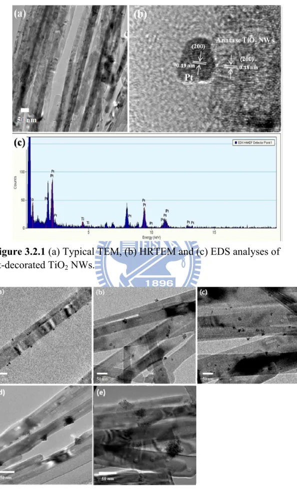
The corresponding XRD patterns. ... 23 Figure 3.2.1 (a) Typical TEM, (b) HRTEM and (c) EDS analyses of
Pt-decorated TiO2 NWs. ... 26
Figure 3.2.2 TEM images of Pt-decorated TiO2 NWs with the Pt contents of (a) 1.0, (b) 2.0, (c) 3.0, (d) 5.0 and (e) 10 wt %. ... 26 Figure 3.3.1 Absorption spectra of MB solutions under different UV
irradiation times by using TiO2 NWs. ... 29
Figure 3.3.2 C/Co versus irradiation time plots for MB photodegradation
under UV illumination by using Pt-decorated TiO2 NWs with
X
Figure 3.4.1 The MB photodegradation results by using different photocatalysts including Pt-loaded, Pt-decorated, Ag-decorated, Au-decorated TiO2 NWs, and P-25 TiO2
powder ... 32 Figure 3.4.2 Recycling test on Pt-decorated TiO2 NWs with Pt content of
3 wt %. ... 32 Figure 3.5.1 SEM images of (a) In2O3-decorated TiO2 NWs (molar ratio
of In2O3 to TiO2 =1:1), and (b) pure In2O3 nanoparticles ... 35
Figure 3.5.2 SEM image of In(OH)3-decorated TiO2 NWs. ... 36
Figure 3.5.3 HRTEM image taken on an individual In2O3-decorated TiO2
NW ... 36 Figure 3.5.4 In2O3-decorated TiO2 NWs with various In2O3/TiO2 molar
ratios of (a) 0.25:1, (b) 0.5:1, (c) 1:1, (d)1.5:1, (e) 2:1, (f) 2.5:1 (g) 5:1 ... 37 Figure 3.6.1 Absorption spectra of RB solutions under different UV
XI
Figure 3.6.2 C/Co versus irradiation time plots for RB photodegradation
under UV illumination by using In2O3-decorated TiO2 NWs
with various In2O3/TiO2 molar ratios ... 40
Figure 3.6.3 The RB photodegradation results under UV light irradiation by using different photocatalysts including In2O3-loaded,
In2O3-decorated, TiO2 NWs and commercial P-25 TiO2
powders ... 41 Figure 3.6.4 Recycling test on In2O3-decorated TiO2 NWs with the
In2O3/TiO2 molar ratio of 1:1. ... 42
Figure 3.7.1 TEM image and the correspding EDS spectra for
In2O3-TiO2-Pt NWs. ... 44
Figure 3.8.1 Band structures and charge transfer event in In2O3-TiO2-Pt
NWs. ... 46 Figure 3.8.2 MB photodegradation results under UV light irradiation by
using In2O3-TiO2-Pt NWs with various Pt contents. ... 46
Figure 3.8.3 Absorption spectra of MB solutions after exposure of 1 h of daytime sunlight (a) without any catalyst and (b) in the
XII
Figure 3.9.1 Photocurrent response of pure TiO2 NWs, In2O3-TiO2 NWs
and In2O3-TiO2-Pt NWs with differernt Pt contents. ... 50
Figure 3.9.2 Illustration of the apparent Fermi level potential of TiO2 in
(a) In2O3-TiO2 and (b) In2O3-TiO2-Pt systems. ... 51
Figure 3.10.1 Charge separation scheme for Pt/In2O3/TiO2 in present of
RB dye. ... 53 Figure 3.10.2 Quenching of photoluminescence emission of RB Dye
(doner) with different samples (acceptors). ... 53 Figure 3.10.3 Time-resolved PL spectra of RB solutions containing In2O3,
In2O3-TiO2 and In2O3-TiO2-Pt samples. ... 56
Table 1 Kinetic analysis of emission decay of RB in the presence of different samples. ... 57
1
Chapter 1. Introduction
1.1 Introduction of TiO
2Titanium dioxide (TiO2) has been widely employed as photocatalytic
materials in the purification and treatment of contaminated air and water owing to its low cost, nontoxicity, and chemical stability [1]. Recently, one-dimensional nanostructures of TiO2 such as nanotubes and nanowires
have attracted intensive research interests because of their dimensionality-dependent physicochemical properties and potential applications in the fields of solar-energy conversion, lithium batteries, and supercapacitors. TiO2 exists in nature as well-known minerals of rutile,
anatase and brookite. Anatase is metastable with respect to rutile and may transform spontaneously into rutile at temperature above 800 ºC [2]. As shown in Figure 1.1, anatase TiO2 possesses relatively negative
conduction band potential that ensures promising activity in many photocatalytic processes. However, its wide bandgap energy (3.2 eV) allows only ultraviolet (UV) absorption. As a result, an effort to modulate the band structure of TiO2 to enable photocatalysis under visible light is
2
Figure 1.1 List of bandgaps of common semiconductors [3].
1.2 One-dimentional TiO
2nanostructures
One-dimensional (1-D) nanostructures including nanowires, nanorods, nanoribbons and nanotubes have been the subject of intensive research due to their potential use as active components or interconnects in nanoscale electronic and electromechanical devices [4]. The space charge region in 1-D nanostructured crystals is well constructed along the longitudinal direction, enabling charge transfer along single direction and thus the facilitation of carrier collections. Furthermore, the pronounced delocalization of charge carriers in 1-D crystals can significantly lower
3
the probability of e--h+ recombination [5]. Consequently, improved photoelectric conversion efficiency such as the photocatalytic activity was regularly observed in 1-D nanostructures when compared with their spherical or particulate counterparts. As shown in Figure 1.2.1, TiO2
nanorods with higher aspect ratios were found to exhibit superior photocatalytic performance as compared to the nanoparticles and short nanorods [5].
Figure 1.2.1 Comparison of photocatalytic efficiency for TiO2 nanorods
4
1.2.1 Previous Studies of 1-D TiO
2nanostructures
There are many synthetic methods to obtain TiO2 in 1-D forms, such
as sol-gel method [6, 7], hydrothermal method [8],solvothermal method [9], direct oxidation process [10], chemical vapor deposition [11], electrochemical deposition [12], and sonochemical method [13]. As one of the Ti-O series products, hydrogen titanate (H2Ti3O7) has draw much
research attention due to its capability of feasible transformation into 1-D TiO2 upon heat treatment. Since the pioneering work by Kasuga et al [14,
15], alkaline hydrothermal approach has been widely employed to produce H2Ti3O7. By using P-25 TiO2 powder as the precursor in
concentrated NaOH solution, various 1-D H2Ti3O7 including nanotubes,
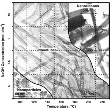
nanosheets, nanowires and nanoribbons can be obtained in high yield. As revealed in Figure 1.2.2, the morphology of H2Ti3O7 in the alkaline
hydrothermal process can be readily controlled by modulating the concentration of NaOH and the reaction temperature. Figure 1.2.3 shows the TEM images of the as-obtained H2Ti3O7 products by using the
alkaline hydrothermal method. A formation mechanism for these 1-D nanostructures of H2Ti3O7 was proposed and illustrated in Figure 1.2.4
5
partially dissolved in NaOH, leaving terraces on their surface. The dissolved atoms recrystallized in sheet-like structures, which further curved up into nanoloops with single-spiral, multiple-spiral, or onion-like cross section. The rest of the bulk crystal was then transformed into nanotubes by oriented crystal growth, supplied with TiO6 building blocks
via the alkaline dismantling of the anatase raw material of TiO2.
Figure 1.2.2 Morphological phase diagram of nanostructures of H2Ti3O7
6
Figure 1.2.3 TEM images of H2Ti3O7 with (A) nanoparticle/nanotube
mixture, (B) nanotubes, (C) nanotube/nanoribbon mixture, (D) and
nanoribbons. Conditions of reaction: (A) 5 mol dm-3 of NaOH at 140 °C, (B) 9 mol dm-3 of NaOH at 160 °C, (C) 5 mol dm-3 of NaOH at 220 °C, and (D) 7.5 mol dm-3 of NaOH at 220 °C [16].
Figure 1.2.4 Schematic illustration for the formation mechanism of H2Ti3O7 nanotubes [17].
7
1.2.2 Recently Studies of 1-D TiO
2Nanostructures
With the open-ended tabulate and layered structures, H2Ti3O7 has
been shown promising in the preparation of diverse 1-D TiO2
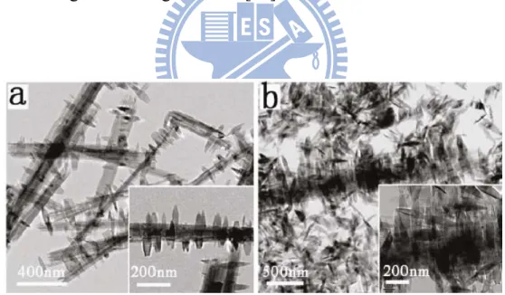
nanostructures. Recently, Wang et al successfully synthesized anatase TiO2 nanoshuttles through the hydrothermal treatment on the
first-prepared H2Ti3O7 NWs [18]. Figure 1.2.5 displays the TEM images
of TiO2 nanoshuttles obtained by controlling the pH value of the reaction
solution. Due to the minimization of total surface energies, TiO2
nanoshuttles were grown with the thermodynamically stable facets of (101) and (001) exposed at their surfaces. The morphology of the final products can be further modulated by controlling the hydrothermal reaction time. As shown in Figure 1.2.6, fishbone-like composite structures can be obtained by prolonging the reaction time to 3 and 6 h. These delicate structures may find practical applications in photocatalysts.
8
Figure 1.2.5 (a) SEM image of H2Ti3O7 NWs. (b,c,d) TEM and ED
results of the anatase TiO2 nanoshuttles. (e,f) TEM and the corresponding
HRTEM images for a single shuttle [18].
Figure 1.2.6 TEM images of the TiO2 products obtained with different
9
1.3 Semiconductor-Metal Composite System
Semiconductor-metal nanocomposites have been widely employed in photocatalysis [19-21]. The overall photocatalytic efficiency of semiconductors can be enhanced by contacting with metals. When semiconductor and metal nanoparticles are in contact, the photoexcited charge carriers re-distribute between the semiconductor and metal domains [22]. This phenomenon promotes the separation of electron-hole pairs. Figure 1.3.1 displays the Fermi level equilibration in a semiconductor-metal nanocomposite system. Within this system, metal may play an important role of storing and shuttling electrons. The photogenerated electrons of semiconductor would thus preferentially transfer to metal domain, leaving positively charged holes in semiconductor to achieve charge carrier separation [23]. Pu et al recently reported a semiconductor-metal composite system of Au-decorated NaxH2-xTi3O7 nanobelts (NBs). The morphological investigation was
shown in Figure 1.3.2 [24]. Due to the band offsets between NaxH2-xTi3O7
and Au, a notable charge separation was expected to take place at the interface of NaxH2-xTi3O7/Au, leading to the enhanced photocatalytic
10
Figure 1.3.1 Fermi level equilibration in a semiconductor-metal nanocomposite system [22]
Figure 1.3.2 (a) Typical TEM image, (b) ED pattern and (c) HRTEM image of Au-decorated NaxH2-xTi3O7 NBs [24].
11
Figure 1.3.3 Photodegradation of thionine under visible irradiation by using Au-decorated NaxH2-xTi3O7 NBs with various Au contents. [24]
1.4 Semiconductor-Semiconductor Composite System
Besides the semiconductor-metal composite system, combination of two semiconductors with appropriate band offsets (type-II heterogeneity) may also improve the charge carrier separation. Kamat et al studied the photoelectrochemical behavior of CdSe/TiO2 composite films and found
an increased photocurrent over the electrode [25]. As shown in Figure 1.4.1, upon light illumination, the photogenerated electrons quickly transferred from CdSe to TiO2 due to the lower conduction band potential
12
interface of CdSe/solution, allowing for oxidation reaction with the redox couple of solution. Combining two different semiconductors has two main advantages: (1) extension of light absorption in a wider range, and (2) retardation of charge carrier recombination.
Figure 1.4.1 Charge crrier dynamis in a coupled semiconductor system [25].
13
Chapter 2. Experimental Section
2.1 Chemicals
All chemicals were analytic grade reagents and used without further purification.
1. P-25 (TiO2), Degussa.
2. Sodium hydroxide (NaOH), 99.995%, Aldrich. 3. Ethanol (CH3CH2OH), 99.5%, Aldrich.
4. Chloropatinic acid hydrate (H2PtCl6),99.995%, Aldrich.
5. Indium (III) chloride (InCl3), 99.99%, Aldrich.
6. Ammonium hydroxide solution (NH4OH), 33%, Aldrich.
7. Chloroauric acid (HAuCl4), 99.99%, Aldrich.
8. Silver nitrate (AgNO3), 99.99%, J.T Baker.
9. Methylene blue, (C16H18N3SCl.3H2O), Aldrich.
10. Rhodamine B, (C28H31ClN2O3), Aldrich.
2.2 Instruments and Principles
1. Scanning Electron Microscope (SEM): The kinetic energy of
accelerated electrons in SEM is dissipated as many different signals when hitting the sample surfaces. These signals mainly include
14
secondary and backscattered electrons. Secondary and backscattered electrons are then collected and used for imaging the morphology and compositional contrast of samples, respectively.
2. Transmission Electron Microscope (TEM): In TEM, the electrons are focused with electromagnetic lenses and transmitted through the sample to image and analyze the microstructure. The electron beams are basically accelerated at several hundred kV, producing wavelength much smaller than that of light. For example, 200 kV of acceleration voltage produces electron beam with a wavelength of 0.025Å. The resolution of TEM is however limited by aberrations inherent in electromagnetic lenses, which is about 1-2 Å.
3. Energy-Dispersive X-Ray Spectroscopy (EDS): EDS is a typical facility of SEM and TEM. It includes a sensitive X-ray detector, a liquid nitrogen cooling system, and software to analyze the energy spectra. An EDS detector contains a crystal that absorbs X-ray by ionization, yielding free electrons in the crystal to produce an electrical charge bias. The signals are then converted into the characteristic X-ray of element to identify the composition of samples.
15
produced through the interaction of the incident X-ray with the sample under the regime of Bragg's Law (nλ = 2d sin θ). This law correlates the wavelength of X-ray (λ) with the diffraction angle (2θ) and the lattice spacing of crystal (d) of the sample. By scanning the sample through a wide 2θ range to collect primary diffraction peaks, one may identify the crystal structure of sample by referring to the standard reference patterns.
5. UV-Visible Spectrophotometer: Absorption of incident radiation by the electrons in materials usually leads to a high frequency, i.e. low wavelength, absorption band that can be observed in the range of 200 to 800 nm. For a solution containing an absorbing substance, the absorptivity ratio at a fixed wavelength is defined as Io/I, which is logarithmically related to the concentration of solute (c) and the optical path length of sample cell (b) according to the Beer Lambert law: Absorbance (A) = log10 (Io/I) = α b c, where α is a constant named
absorption coefficient.
6. Photoluminescence Spectroscope: When materials are exposed to X-ray, γ- ray or light with sufficiently high energy, ionization of atoms takes place to remove the electrons from their orbits, rendering
16
the electronic structure of the atoms unstable. The electrons in higher orbit may then "fall" into the lower one to fill the hole left behind. During the falling process, energy with an equal amount to the energetic difference between the two orbits will be released in the form of photon to emit radiation.
2.3 Preparation of Anatase TiO
2Nanowires
Commercial TiO2 powder (Degussa P-25) was used as the starting
material. In a typical process, 1.0 g of Degussa P-25 was first dispersed in 10 mL of absolute ethanol, and then mixed with 10 mL of 10 M NaOH aqueous solution under vigorous stirring for 10 min. The mixed solution was transferred into a Teflon-line stainless-steel autoclave. Subsequently, the autocalve was heated and maintained at 200oC for 24 h, and then cooled to room temperature naturally. The resultant white slurry was washed with deionized water and HCl aqueous solution (pH=1) until the pH value is below 7. A complete removal of Na constituent can be achieved through this acid-washing process [26], which resulted in the formation of H2Ti3O7 NWs. These NWs were then annealed in air at 700 o
17
2.4 Preparation of Pt-decorated TiO
2NWs
To decorate NWs with Pt nanoparticles, 5 mg of anatase TiO2 NWs
were dispersed in 20 mL absolute ethanol, followed by the addition of 50 μL H2PtCl6 (5 mM) with vigorous stirring. The mixed solutionin quartz
tube was irradiated by UV light (with the wavelength of 365 nm) for 30 min to generate electros for reduction of Pt ions. Note that ethanol was used as the sacrificial reagent for the photogenerated holes. The product (TiO2-Pt NWs with the Pt content of 1.0 wt %) was centrifuged, washed
with deionized water and ethanol, and then dried at 60oC in air. In this work, two other novel metals (Ag and Au) were also deposited on NW surfaces, with which we may learn the effects of various metal decorations on the photocatalytic properties of TiO2. For the synthesis of
Au-decorated anatase TiO2 NWs, HAuCl4 was used as the Au source,
followed by the same procedure performed in the preparation of Pt-decorated sample. As to the fabrication of Ag-decorated anatase TiO2
NWs, AgNO3 was used as the Ag source, followed by the same procedure
18
2.5 Preparation of In
2O
3-decorated TiO
2NWs
To prepare In2O3-decorated TiO2 NWs, 221.18 mg of InCl3 powder
was first dissolve in 5 mL deionized water, followed by the addition of 500 µL NH4OH solution. After stirring for 10 min, TiO2 NWs of 40 mg
were added into the above solution. The mixed solution was then stirred for 12 h at room temperature. The resultant white precipitation was collected and washed with deionized water for several times. After dried in air at 60oC, the white powder was further annealed in air at 700 oC for 2 h to produce In2O3-decorted TiO2 NWs (In2O3-TiO2).
2.6 Preparation of Pt and In
2O
3co-decorated TiO
2NWs
To prepare the Pt and In2O3 co-decorated TiO2 NWs, 5 mg of
In2O3-TiO2 NWs were dispersed in 20 mL absolute ethanol in a quartz
tube first. H2PtCl6 of a suitable amount (5 mM) was then added into the
quartz tubes and irradiated by UV light (with the wavelength of 365 nm) for 30 min to grow Pt nanoparticles on the surfaces of TiO2. The product
was centrifuged, washed with deionized water and ethanol, and then dried at 60oC in air.
19
2.7 Photocurrent Measurement
Photocurrent measurement was conducted in a photoelectrochemical system under white light irradiation (xenon lamp, 500 W, with a light intensity of 175 mW/cm2). NW film, well adhered to FTO substrates, was prepared by dripping NW suspensions of sufficient amount onto FTO glasses, followed by a heat treatment to remove the solvent. The NW film on FTO substrate was used as the photoanode in the three-electrode cell which consisted of Pt counter electrode, Ag/AgCl reference electrode, and 0.01 M NaOH redox couple.
2.8 Photocatalytic Activity Study
Photodegradation of ethylene blue (MB) and rhoamine B (RB) were monitored to test the photocatalytic activity of the NW samples. Irradiation was provided by UV lamps (8W) with a wavelength of 365 nm. In a typical experiment, 5.0 mg of photocatalyst was added into 20 mL of MB (or RB) solution in the photoreactor vessel. The concentrations of MB and RB in the presence of NWs under illumination were both 1.0×10⁻⁵ M. At certain time intervals of irradiation, 1.5 mL of the reaction solution was withdrawn and centrifuged to remove the photocatalyst particles. The filtrates were
20
analyzed with a UV-Visible spectrophotometer to measure the concentration variation of dye through recording the corresponding absorbance of the characteristic peak. To investigate the recyclability and stability of photocatalysts, three cycles of photocatalytic reactions were conducted by using In2O3-TiO2-PtNWs with the Pt content of 5.0 wt % as
the representative sample. The photodegradation of MB (1.0×10⁻⁵ M) under natural sunlight was also examined.
2.9 Photoluminescence Lifetime Measurement
Time-resolved photoluminescence (PL) spectra were measured using a home-built single photon counting system. Diode laser (375 nm) with the pulse duration of 50 ps was used as the excitation source. The signals collected at the excitonic emission of RB (λ = 581 nm) were dispersed with a grating spectrometer, detected by a high-speed photomultiplier tube, and then correlated using a single photon counting card. The emission decay data were analyzed with the biexponential kinetics in which two decay components were derived. The lifetimes (τ1 and τ2), pre-exponential factors
21
summarized for RB (1μM), RB/In2O3 (1mg in 1μM RB), RB/In2O3-TiO2
(2mg in 1μM RB) and RB/ In2O3-TiO2-Pt (2mg in 1μM RB).
2.10 Characterization
The morphology and dimensions of the products were examined with a field-emission SEM (FESEM, JEOL, JSM-6500F). The crystallographic structure of the samples was investigated with XRD (Burker, D2 phaser) and a high-resolution TEM (HRTEM, JEOL, JEM-2010) operated at 200 kV. The compositional information was obtained with an EDS, an accessory of the TEM (JEM-2010). UV-Visible absorption spectra were obtained using a Hitachi U-3900H at 25oC under ambient atmosphere. For PL spectroscopy, a Hitachi F-4500 equipped with a xenon lamp (150W) was used. Photocurrent measurement for the TiO2 NWs film was measured
by using an electrochemical workstation (Jiehan 5600, Taiwan) under a xenon lamp (500W, 175mW/cm2) illumination.
22
Chapter 3. Results and Discussion
3.1 Structural Investigation on TiO
2NWs
Figure 3.1.1 shows the SEM images and XRD patterns of H2Ti3O7
and anatase TiO2 NWs. The as-prepared H2Ti3O7 NWs have a typical
diameter of 70-150 nm and length up to a few μm. After calcinated at 700oC for 4h, a dehydration reaction occurred to H2Ti3O7, resulting in the
formation of anatase TiO2. This phase transformation can be confirmed
by the corresponding XRD analyses shown in Figure 3.1.1(c) [27]. Note that a similar morphology to that of the H2Ti3O7 NWs was found for the
anatase TiO2 which preserved the NW structures with the diameter of
23
Figure 3.1.1 SEM images of (a) H2Ti3O7 and (b) anatase TiO2 NWs. (c)
The corresponding XRD patterns.
3.2 Decoration of Pt on TiO
2NWs
To extract the photoexcited electrons from TiO2 NWs for
participation in photocatalytic reduction reaction, we introduced an electron-acceptor, Pt, at the surfaces of NWs. We used the photodeposition method to deposit Pt nanoparticles onto TiO2 NWs. As
24
presented on NW surfaces after the photodeposition process. The HRTEM image, shown in Figure 3.2.1 (b), clear reveals an interlayer spacing of 1.89 Å in the NW region, in good agreement with the d spacing of the (200) lattice planes of anatase TiO2 [28]. In the particle
region, an interlayer spacing of 1.93 Å was obtained, complying with the lattice spacing of (200) planes of the fcc Pt [29]. With increasing the amount of H2PtCl6, the density of Pt nanoparticles grown at the surfaces of
NWs was gradually increased (Figure 3.2.2). These Pt nanoparticles however have irregular shape and would aggregate once the concentration of H2PtCl6 becomes relatively high. It should be noted that no
free-standing Pt nanoparticles were observed in the products, demonstrating the advantage of the current approach to obtain metal nanoparticle-decorated NWs. A growth mechanism for the formation of Pt nanoparticles was proposed as follows (equations 1 to 5) [30-32]. Irradiation for PtCl62- ions under UV light would transform them into
PtCl42- and then Pt0 (equation 1). The photodeposition process of Pt on
NWs mainly followed the three steps: (1) transformation of PtCl62-into
PtCl42-, (2) dissociation of Cl from PtCl42-, followed by the reduction of
25
association of Pt0-Pt0 [32]. Here ethanol plays an important role of accepting photogenerated holes of NWs and facilitating the formation of PtCl42- (equations 2 to 5) [31]. PtCl6 2- → PtCl42- → Pt0 (Eq. 1) PtCl62- + RCH2OH + hν → PtCl63- + ‧RCH2O + H+ (Eq. 2) PtCl63- ↹ PtCl52- + Cl- (Eq. 3) PtCl52- + ‧RCH2O → PtCl42- + RCH2=O + HCl (Eq. 4) 2PtCl52- ↹ PtCl62- + PtCl42- (Eq. 5)
Based on the above interpretation, we believed that the present photodeposition approach can be extended to obtain other novel metal-decorated NWs such as Ag- and Au-decorated samples [33-35]. With these samples, we may learn the effects of various metal decorations on the photocatalytic properties of TiO2 NWs.
26
Figure 3.2.1 (a) Typical TEM, (b) HRTEM and (c) EDS analyses of Pt-decorated TiO2 NWs.
Figure 3.2.2 TEM images of Pt-decorated TiO2 NWs with the Pt contents
27
3.3 Photocatalytic Properties of Pt-decorated TiO
2NWs
MB, a typical textile dye, was used as the model contaminant for photocatalysis here. Since MB is a cationic dye that may accept electrons from photocatalysts upon light illumination, we may realize the electron transfer event from TiO2 to Pt for the present Pt-decorated TiO2 NWs.
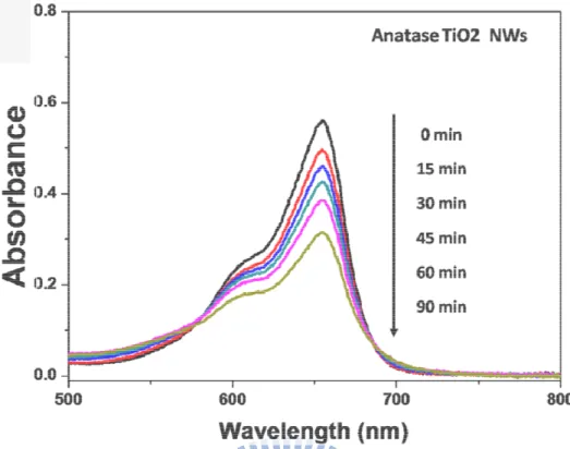
Note that ethanol was used as the sacrificial holes scavenger for photocatalyst to facilitate the further utilization of photoexcited electrons. Figures 3.3.1 represents the time-depended UV-Visible spectra of MB solutions under UV illumination in the presence of pristine TiO2 NWs. It
can be seen that the intensity of the characteristic absorption peak decreased with the irradiation time [36]. The bleaching of the absorption at 654 nm implies the reduction of MB and thus the operation of photocatalysis by using NWs. We then analyzed the normalized concentration of MB (C/Co) as a function of irradiation time in order to
understand the progress of MB photodegradation (Figure 3.3.2). As compared to pure NWs, Pt-decorated samples exhibit superior photocatalytic efficiency toward MB photodegradation. This improvement mainly resulted from the deposited Pt that can promote charge separation by attracting the photoexcited electrons from NWs, thus providing more
28
electrons for the decomposition of MB. As increasing the amount of Pt from 1 to 3 wt%, an enhanced photocatalytic activity was found for TiO2
NWs correspondingly. However, an obvious decrease in the photocatalytic activity was observed when Pt content was increased from 5 to 10 wt %. This outcome demonstrated an optimal content of Pt decoration for improving the photocatalytic performance of TiO2 NWs. It has been
widely documented that the excess content of metal may cover a large part of photocatalyst surfaces, which in turn decreases the number of active sites for photocatalysis as well as retards the access of light irradiation to photocatalyst surfaces [37]. Both of the above two situations may account for the depressed photocatalytic efficiency as observed here.
29
Figure 3.3.1 Absorption spectra of MB solutions under different UV irradiation times by using TiO2 NWs.
Figure 3.3.2 C/Co versus irradiation time plots for MB photodegradation
under UV illumination by using Pt-decorated TiO2 NWs with various Pt
30
3.4 Effects of Various Metal Decorations and Recycling Test
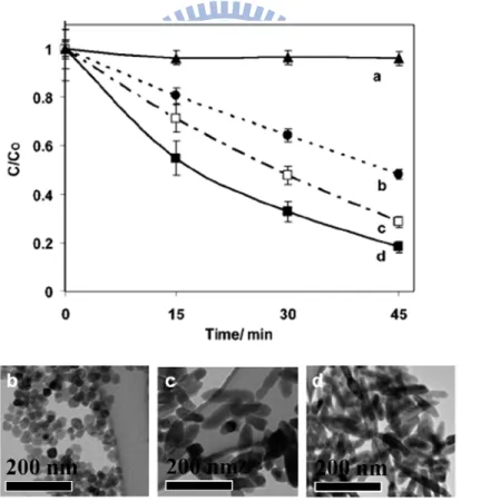
To further demonstrate the remarkable photocataytic properties for the present Pt-decorated samples, five kinds of photocatalysts including Pt-loaded, Au-decorated, Ag-decorated, Pt-decorated TiO2 NW, and P-25
TiO2 powder were compared in MB photodegradation under the same
conditions. Note that Pt-loaded sample was prepared by simply mixing NWs with Pt colloids, which led to the random distribution of Pt around TiO2. As to the preparation of Au- and Ag-decorated NWs, a similar
approach to the synthesis of Pt-decorated sample was used. The comparative results were shown in Figure 3.4.1, from which several points can be observed. First, Pt-loaded sample did not perform as better as Pt-decorated NWs did, presumably owing to the less contact of Pt with NWs in Pt-loaded sample. Because of the limited contact between Pt and TiO2 NWs, a retarded charge separation was expected for Pt-loaded NWs
sample, thus leading to the lower photocatalytic activity. Second, as compared to the Ag- and Au-decorated samples, Pt-decorated NBs exhibited superior photocatalytic efficiency toward MB photodegradation, which can be explained by the difference of work function among the deposited metals. Among the three metals, Pt has the largest work
31
function [38], which means that the difference between the conduction band of TiO2 and the Fermi level of metal was the largest in Pt-decorated
case. It had been pointed out that the driving force of electron transfer from semiconductor to metal is proportional to such energetic difference. In the current case, Pt-decorated TiO2 NWs may possess higher driving
force for charge separation and consequently showed better photocatalytic efficiency as compared to Ag- and Au-decorated samples. Third, as compared to the commercial product like P-25 TiO2 powder,
Pt-decorated TiO2 NWs showed better photocatalytic performance,
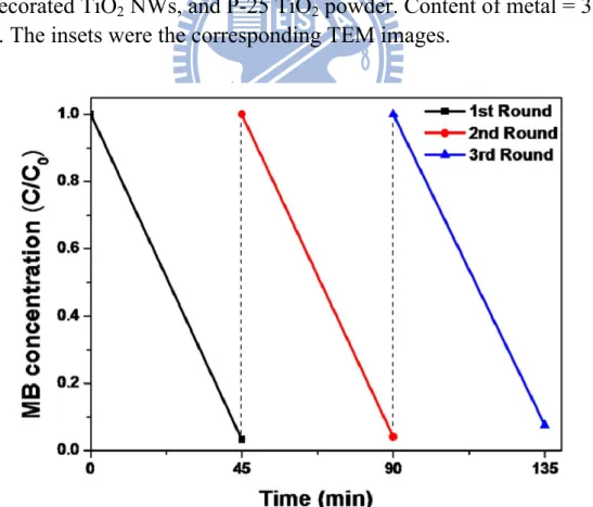
demonstrating their potential as an efficient photocatalyst in relevant redox reactions. We performed a recycling test by using Pt-decorated TiO2 NWs
with the Pt content of 3 wt % to investigate their recyclability and stability. As shown in Figure 3.4.2, no obvious decay of photocatalytic efficiency was found for Pt-decorated NWs after being repeatedly used for three times in MB photodegradation. This result shows that the present Pt-decorated TiO2 NWs had excellent stability and could be
32
Figure 3.4.1 The MB photodegradation results by using different photocatalysts including Pt-loaded, Pt-decorated, Ag-decorated,
Au-decorated TiO2 NWs, and P-25 TiO2 powder. Content of metal = 3.0
wt %. The insets were the corresponding TEM images.
Figure 3.4.2 Recycling test on Pt-decorated TiO2 NWs with Pt content of
33
3.5 Decoration of In
2O
3on TiO
2NWs
On the other hand, we may provide TiO2 NWs with an appropriate
hole-acceptor to scavenge the photogenerated holes of TiO2 for
photocatalytic oxidation purpose. Through a precipitation-annealing process, we could decorate TiO2 NWs with In2O3 nanoparticles which had
suitable band structures to allow hole transfer from TiO2 to In2O3 (Ecb=
-0.62V, Evb= 2.18V vs. NHE for In2O3; Ecb= -0.29V, Evb= 2.91V vs.
NHE for anatase TiO2) [39]. As shown in Figure 3.5.1 (a), the diameter of
In2O3 nanoparticles grown at the surfaces of TiO2 NWs was about 20~50
nm. The corresponding XRD analysis shown in Figure 3.5.1 (c) confirmed the crystal structure of In2O3 nanoparticles. Note that pure
In2O3 nanoparticles can also be obtained by using the same procedure
without the addition of NWs. Figure 3.5.1 (b) displays the morphology of the single-phase In2O3 nanoparticles. The dimension and shape of the
pure In2O3 nanoparticles were similar to those deposited at the surfaces of
NWs, with which we may make a fair comparison of their photocatalytic properties.
The decoration of TiO2 NWs with In2O3 nanoparticles was achieved
34
NH4OH solution, white precipitation of an abundant amount rapidly
formed within the solution. The corresponding XRD analysis show that the precipitated particles were made of In(OH)3, which resulted from the
reaction of InCl3 with NH4OH. Subsequently, TiO2 NWs of a given
amount were added into the above solution and the mixed solution was stirred for 12 h to allow the attachment of In(OH)3 nanoparticles onto the
surfaces of TiO2 NWs. SEM investigation shown in Figure 3.5.2 clearly
reveals the decoration of NWs with a lot of nanoparticles of In(OH)3.
During the stirring process, it was expected that In–OH bonds of In(OH)3
nanoparticles would bind to the unsaturated oxygen at TiO2 surfaces to
form Ti–O–In–OH linkage, which further led to the attachment of In(OH)3 onto TiO2 NWs [40]. These In(OH)3-decorated NWs were then
annealed at 700oC in air for 2 h to transform In(OH)3 into In2O3 through a
dehydration process. As a result, In2O3-decorated TiO2 NWs were
obtained. The HRTEM image taken at the interface of NW and nanoparticle regions of In2O3-TiO2 NWs clearly reveals two distinct sets
of lattice fringes (Figure 3.5.3). An interlayer spacing of 0.18 nm was observed in the NW region, in good agreement with the d spacing of the (200) lattice planes of TiO2 [28]. In the particle region, interlayer spacings
35
of 0.29 nm and 0.41nm were obtained, complying with the lattice spacing of (222) and (211) planes of the bcc In2O3, respectively [41]. Figures
3.5.4 reveals the gradual increase in In2O3 particle density for
In2O3-decorated TiO2 NWs, which was achieved by employing InCl3 of
increasing amounts. As increasing the amount of InCl3, the resultant
surface-attached In2O3 particles became prevalent and aggregated on NW
surfaces.
Figure 3.5.1 SEM images of (a) In2O3-decorated TiO2 NWs (molar ratio
of In2O3 to TiO2 =1:1), and (b) pure In2O3 nanoparticles. The
36
Figure 3.5.2 SEM image of In(OH)3-decorated TiO2 NWs.
Figure 3.5.3 HRTEM image taken on an individual In2O3-decorated TiO2
NW. The interface between TiO2 and In2O3 was highlighted with a
37
Figure 3.5.4 In2O3-decorated TiO2 NWs with various In2O3/TiO2 molar
38
3.6 Photocatalytic Properties of In
2O
3-decorated TiO
2NWs
To investigate the photocatalytic properties of In2O3-decoarted TiO2
NWs, RB was used as the test pollutant since it could react with photogenerated holes to get decomposed through a photocatalytic oxidation process. Note that the oxygen dissolved in water may act as the sacrificial electron consumer for photocatalyst to facilitate the further utilization of photogenerated holes. The time-dependent UV-visible spectra of RB solutions under UV illumination in the presence of TiO2
NWs were first shown in Figure 3.6.1. It can be seen that the intensity of the characteristic absorption peak at 554 nm [42] decreased dramatically with the irradiation time, implying the successful degradation of RB by the photocatalysis of TiO2. Figure 3.6.2 displays the photodegradation
results by using In2O3-decorated TiO2 NWs with different In2O3/TiO2
molar ratios. The photocatalytic efficiency of TiO2 NWs was enhanced as
increasing the molar ratio of In2O3/TiO2 from 0.25 to 1.0. This
enhancement mainly came from the deposited In2O3 that can promote
charge separation by attracting more photogenerated holes from TiO2 NWs,
thus providing more holes for the decomposition of RB. When the molar ratio of In2O3/TiO2 was further increased to 2.5 and 5.0, a decrease in the
39
photocatalytic activity was however observed for TiO2 NWs. This
depression might result from the excess In2O3 nanoparticles which may
cover a large part of NW surfaces to block the light absorption of TiO2
[43]. As a result, an unfavorable effect, analogous to that of excess metal loading, would emerge to hinder the resulting photocatalytic performance of TiO2. Although In2O3 itself may still absorb light to generate charge
carriers, the efficiency for these charge carriers to participate in photocatalysis was actually poor, as can be clearly seen in Figure 3.6.2.
Figure 3.6.1 Absorption spectra of RB solutions under different UV irradiation times by using TiO2 NWs.
40
Figure 3.6.2 C/Co versus irradiation time plots for RB photodegradation
under UV illumination by using In2O3-decorated TiO2 NWs with various
In2O3/TiO2 molar ratios. The results by using pure TiO2 NWs and pure
In2O3 nanoparticles were also included for comparison.
To demonstrate the remarkable photocatalytic properties for In2O3-decorated TiO2 NWs, further comparative experiments were
conducted. In Figure 3.6.3, three different photocatalysts including In2O3-loaded, In2O3-decorated TiO2 NWs, and P-25 TiO2 powder were
used and compared. Note that In2O3-loaded NWs were prepared by simply
mixing NWs with In2O3 nanopartilces, resulting in a random distribution of
In2O3 nanoparticles around NWs. The as-prepared In2O3-decroated NWs
exhibited superior photocatalytic performance as compared to the other two samples. This is due to the pronounced charge separation which was
41
believed to occur at the interface of In2O3/TiO2 in In2O3-decorated TiO2
NWs. Furthermore, these In2O3-decorated NWs were used in the
recycling photocatalytic operation to test their recyclability and stability. As shown in Figure 3.6.4, after being repeatedly used for three times in RB photodegradation, no obvious decay of photocatalytic efficiency was observed. This result demonstrates that the present In2O3-decorated TiO2
NWs could be promisingly utilized in the long-term course of photocatalysis.
Figure 3.6.3 The RB photodegradation results under UV light irradiation by using different photocatalysts including In2O3-loaded, In2O3-decorated,
TiO2 NWs and commercial P-25 TiO2 powders. Molar ratio of In2O3/TiO2
42
Figure 3.6.4 Recycling test on In2O3-decorated TiO2 NWs with the
In2O3/TiO2 molar ratio of 1:1.
3.7 Further Decoration of Pt on In
2O
3-TiO
2NWs
To further promote the photocatalytic efficiency of TiO2, we applied
both Pt and In2O3 decorations for TiO2 NWs. Due to the difference in
band structures between In2O3 and TiO2, the photogenerated holes in TiO2
would preferentially transfer to In2O3, leaving photoexcited electrons in
TiO2 domain to achieve charge separation. We can then utilize this
characteristic to deposit Pt at the TiO2 region of In2O3-TiO2 NWs by
using the photodeposition method described in section 3.2. Figure 3.7.1 displays the TEM images of In2O3-decorated TiO2 NWs after they were
43
treated with the Pt photodeposition process. The TEM-EDS results shown in Figure 3.7.1 clearly reveal the deposition of Pt nanoparticles at TiO2
region of In2O3-TiO2 NWs. This outcome reaffirms our proposition that
In2O3 can attract photogenerated holes of TiO2 to leave photoexcited
electrons in TiO2. Upon UV light irradiation, the photoexcited electrons
in TiO2 region of In2O3-TiO2 NWs can then react with the surrouding
PtCl62- ions to grow Pt nanoparticles, resulting in the deposition of Pt at
44
Figure 3.7.1 TEM image and the correspding EDS spectra for In2O3-TiO2-Pt NWs.
3.8 Photocatalytic Properties of In
2O
3-TiO
2-Pt NWs
To demonstrate the even superior photocatalytic performance for In2O3-TiO2-Pt NWs, MB which can serve as an electron-acceptor was
45
again used as the test pollutant here. The band structures shown in Figure 3.8.1 illustrate the charge transfer event that occurred in In2O3-TiO2-Pt
NWs and the subsequent photocatalysis to decompose MB. We expected that much more photoexcited electrons can be extracted from In2O3-TiO2-Pt NWs, which may further lead to the enhanced
photocatalytic efficiency toward MB photodegradation. As shown in Figure 3.8.2, an even better performance of photocatalysis was observed for In2O3-TiO2 NWs once they were decorated with Pt. There again
existed an optimal content of Pt (5.0 wt% here) for improving the photocatalytic efficiency of In2O3-TiO2 NWs. Above this optimal value,
the photocatalytic efficiency of NWs was depressed due to the excess coverage of Pt on TiO2 surfaces.
46
Figure 3.8.1 Band structures and charge transfer event in In2O3-TiO2-Pt
NWs.
Figure 3.8.2 The MB photodegradation results under UV light irradiation by using In2O3-TiO2-Pt NWs with various Pt contents.
47
Since In2O3 has a direct bandgap energy of 2.8 eV, the current
In2O3-TiO2-Pt NWs may be sensitized by In2O3 to absorb visible light and
perform photocatalysis. To explore the applicability of these NWs under visible light illumination, their phtocatalytic performance under natural sunlight was evaluated. As illustrated in Figure 3.8.3, after exposure to 1 h of daytime sunlight, MB was totally degraded by using In2O3-TiO2-Pt
NWs, accompanied with an obvious decoloration of the resultant solution. This result shows that the current In2O3-TiO2-Pt NWs can be used as
highly efficient photocatalysts which may practically harvest energy from sunlight.
48
Figure 3.8.3 Absorption spectra of MB solutions after exposure of 1 h of daytime sunlight (a) without any catalyst and (b) in the presence of
In2O3-TiO2-Pt NWs. Content of Pt = 5.0 wt %. Insets show the
corresponding solution color.
3.9 Photocurrent Measurement for In
2O
3-TiO
2-Pt NWs
To further elucidate the effect of Pt on the charge separation of In2O3-decorated TiO2 NWs, we compared the photocurrent response of
pure TiO2 NW, In2O3-TiO2 NW, and In2O3-TiO2-Pt NW electrodes by
inserting them in a photoelectrochemical cell. Figure 3.9.1 depicts the photocurrent generation for the three kinds of NW electrodes subjected to the white light irradiation. There were several points to be observed from the figure. First, all the electrodes showed prompt response to the on/off
49
cycles of light illumination, demonstrating the effective charge transfer and successful electron collection for the samples within the photoelectrochemical cell. Second, the photocurrent of TiO2 NWs was
significantly enhanced if they were decorated with In2O3. The significant
retardation of charge recombination in In2O3-TiO2 NWs accounted for
such a drastic photocurrent enhancement [44]. Third, a much higher photocurrent was produced when In2O3-TiO2 NWs were further decorated
with Pt of 1.0 wt%. This outcome arose from the increasing driving force of electron transfer from In2O3 to TiO2 achieved by the decoration of Pt
on TiO2 surfaces. Note that semiconductor-metal heterostructures would
undergo a Fermi level equilibration due to the accumulation of photexcited electrons in metal [45]. The equilibrated Fermi level of such composite system appeared to be lower in potential (less negative) than that of the corresponding pure semiconductor. As illustrated in Figure 3.9.2, the apparent Fermi level of TiO2 in In2O3-TiO2-Pt NWs (EF**) was
presumably lower in potential than that of TiO2 in In2O3-TiO2 NWs (EF*).
A larger energetic difference in Fermi levels between In2O3 and TiO2 was
thus expected for In2O3-TiO2-Pt NW system, which in turn promote the
50
an enhancement in the resulting photocurrent production was observed for In2O3-TiO2-Pt NWs. The photocurrent generated from In2O3-TiO2-Pt
NWs was however depressed as the content of Pt was increased to 5.0 and 10 wt%. We supposed that too much Pt deposited on TiO2 of
In2O3-TiO2 NWs would trap the photoexcited electrons in a considerably
high amount, thus leading to a decreased number of electrons that were collected by the external voltammeter.
Figure 3.9.1 Photocurrent response of pure TiO2 NWs, In2O3-TiO2 NWs
51
Figure 3.9.2 Illustration of the apparent Fermi level potential of TiO2 in
52
3.10 Time-Resolved Photoluminescence Spectra
If the observed photocurrent enhancement with the decoration of Pt (1.0 wt%) on In2O3-TiO2 NWs indeed involved the increasing driving
force of electron transfer from In2O3 to TiO2, we should be able to reveal
this event in the corresponding emission decay profiles. Since RB has the band structure that can well fit to In2O3 to allow charge transfer, it was
used as the sensitizer to monitor the charge transfer event among In2O3,
TiO2 and Pt (Figure 3.10.1). As shown in Figure 3.10.2, a significant
quenching in the PL emission of RB was observed for In2O3 as compared
to pure RB. Such quenching became more noticeable in In2O3-TiO2 and
even more significant in In2O3-TiO2-Pt sample, implying the successful
53
Figure 3.10.1 Charge separation scheme for Pt/In2O3/TiO2 in present of
RB dye.
Figure 3.10.2 Quenching of photoluminescence emission of RB Dye (donor) with different samples (acceptor).
54
Figure 3.10.3 shows the time-resolved PL spectra for the three RB solutions relatively containing In2O3, In2O3-TiO2, and In2O3-TiO2-Pt NWs.
The emission decay data were analyzed with biexponential kinetics in which two decay components were derived. The lifetimes (τ1 and τ2),
pre-exponential factors (A1 and A2), and intensity-average lifetime (<τ>)
were determined and summarized in Table 1. The average lifetimes of In2O3, In2O3-TiO2 and In2O3-TiO2-Pt were 1.2171, 1.0472, and 0.6770 ns,
respectively. Note that the difference in the average emission lifetime between In2O3-TiO2 (<τ> = 1.0472 ns) and In2O3 (<τ> = 1.2171 ns)
indicates the emergence of a nonradiative pathway from the interaction between In2O3 and TiO2. This proposition can be confirmed by the more
pronounced emission quenching of RB observed for In2O3-TiO2 sample.
Such difference became more noticeable as In2O3-TiO2 NWs were further
decorated with Pt (<τ> = 0.6770 ns for In2O3-TiO2-Pt versus <τ> = 1.2171
ns for In2O3), inferring a much more significant electronic interaction
between In2O3 and TiO2. If electron transfer was the predominant process
that dictated the emission quenching of RB, we can then estimate the electron-transfer rate constants (ket) of In2O3-TiO2 and In2O3-TiO2-Pt
55
)
(
1
)
(
1
3 2 2 3 2 1 ,In
O
TiO
In
O
k
et
)
(
1
)
(
1
2 3 2 2 3 2 2 ,In
O
TiO
Pt
In
O
TiO
k
et
Using the lifetime values listed in Table 1, we obtained the electron-transfer rate constants from In2O3 to TiO2 (ket,1) and from TiO2 to
Pt (ket,2) as 0.13×10⁹ and 0.52×10⁹ s-1, respectively. In addition, we
noticed that the rate constant of ket,1′ (0.65× 10⁹) was larger than ket,1(0.13
× 109), which means that the electron transfer from In2O3 to TiO2 was
faster in the In2O3-TiO2-Pt system. This result, together with those of
photocatalysis, photocurrent measurement and PL quenching, confirms our suggestion that an increasing driving force of electron transfer from In2O3 to TiO2 can be achieved by the decoration of Pt on the TiO2 region
56
Figure 3.10.3 Time-resolved PL spectra of RB solutions containing In2O3,
57
Table 1Kinetic analysis of emission decay of RB in the presence of different samples. system A1 τ1 (ns) A2 τ2 (ns) <τ> (ns) ket (s -1) RB/In2O3 3213.4 1.4048 6318 0.1224 1.2171 ket,1=0.13 × 10⁹ RB/In2O3-TiO2 1995.1 1.4917 9259 0.1627 1.0472 RB/In2O3 3213.4 1.4048 6318 0.1224 1.2171 ket,1′=0.65× 10⁹ RB/In2O3-TiO2 -Pt 846 1.4454 11031 0.1665 0.6776 RB/In2O3-TiO2 1995.1 1.4917 9259 0.1627 1.0472 ket,2=0.52× 10⁹ RB/In2O3-TiO2 -Pt 846 1.4454 11031 0.1665 0.6776
58
Chapter 4. Conclusion
In this thesis, we have successfully synthesized In2O3-decorated
anatase TiO2 NWs via a simple precipitation-annealing process. The
difference in band structures between In2O3 and TiO2 provided charge
carriers with another preferential route for charge transfer, resulting in the separation of photoexcited electrons and holes. The charge carrier separation in In2O3-TiO2 NWs was revealed with the photocatalytic
decomposition of RB. As compared to the commercial P-25 TiO2 powder
and In2O3-loaded TiO2 NW samples, the as-synthesized In2O3-TiO2 NWs
exhibited superior photocatalytic efficiency under UV illumination, demonstrating their potential as an efficient photocatalyst in relevant redox reactions. A further enhancement in the photocatalytic activity of In2O3-TiO2 NWs can be achieved when Pt nanoparticles of suitable
amount were deposited on the surface of TiO2. This improvement is due
to the increasing driving force of electron transfer from In2O3 to TiO2
achieved by the decoration of Pt on TiO2 surfaces. Time-resolved PL data
showed that a higher electron-transfer rate constant from In2O3 to TiO2
was observed for In2O3-TiO2-Pt NWs, consistent with the results of
59
NWs may find promising photocatalytic applications, especially in the photocatalytic decomposition of various organic pollutants. The present study also gives rise to a new class of highly efficient metal/semiconductor hybrid photocatalysts which may effectively utilize the solar power.
60
Reference
[1] Zhu, J.; Yang, D.; Geng, J.; Chen D.; Jiang Z. J. Nanopart. Res. 2008,
10, 729.
[2] Tang, H.; Berger, H.; Schmid, P. E.; Lévy, F. Solid State Commun. 1993, 87, 847.
[3] Grätzel, M. Nature. 2001, 414, 338.
[4] Duan, X.; Huang, Y.; Cui, Y.; Wang, J.; Lieber, C. M. Nature (London) 2001, 409, 66.
[5] Yun, H. J.; Lee, H.; Joo, J. B.; Kim, W.; Yi, J. J. Phys. Chem. C 2009,
113, 3050.
[6] Miao, L.; Tanemura, S.; Toh, S.; Kaneko, K.; Tanemura, M. J. Cryst.
Growth 2004, 264, 246.
[7] Cozzoli, P. D.; Kornowski, A.; Weller, H. J. Am. Chem. Soc. 2003,
125, 14539.
[8] Zhang, Q.; Gao, L. Langmuir 2003, 19, 967.
[9] Wang, Q.; Wen, Z.; Li, J. Inorg. Chem. 2006, 45, 6944. [10] Wu, J. M. J. Cryst. Growth 2004,269,347.
[11] Wu, J. M.; Shih, H. C.; Wu, W. T. Chem. Phys. Lett. 2005, 413, 490. [12] Liu, S.; Huang, K. Sol. Energy Mater. Sol. Cells 2005, 85, 125.
61
[13] Zhu, Y.; Li, H.; Koltypin, Y.; Hacohen, Y. R.; Gedanken, A. Chem.
Commun. 2001, 2616.
[14] Kasuga, T.; Hiramatsu, M.; Hoson, A.; Sekino, T.; Niihara K.
Langmuir 1998, 14, 3160.
[15] Kasuga, T.; Hiramatsu, M.; Hoson, A.; Sekino, T.; Niihara, K. Adv.
Mater. 1999, 11, 1307.
[16] Waclawik, E. R.; Frost, R. L.; Zhu, H. Y.; Morgan, D. L. Chem. Mater. 2008, 20, 3800.
[17] Kukovecz, A.; Hodos, M.; Horvath, E.; Radnoczi, G.; Konya, Z.; Kiricsi, I. J. Phys. Chem. B 2005, 109, 17781.
[18] Wang, H.; Shao, W.; Gu, F.; Zhang, L.; Lu, M.; Li, C. Inorg. Chem. 2009, 48, 9732
[19] Kraeutler, B.; Bard, A. J. J. Am. Chem. Soc. 1978, 100, 4317. [20] Baba, R.; Nakabayashi, S.; Fujishima, A.; Honda, K. J. Phys. Chem.
1985, 89, 1902.
[21] Kamat, P. V. J. Phys. Chem. B 2002, 106, 7729. [22] Kamat, P. V. J. Phys. Chem. C 2008, 112, 18737
[23] Subramanian, V.; Wolf, E. E.; Kamat, P. V. J. Am. Chem. Soc. 2004,
62
[24] Pu, Y. C.; Chen, Y. C.; Hsu, Y. J. Appl. Catal. B-Environ. 2010, 97 389.
[25] Liu, D.; Kamat, P. V J. Phys. Chem. 1993, 97, 10769.
[26] Jitputti, J.; Suzuki, Y.; Yoshikawa, S. Catal. Commun. 2008, 9, 1265. [27] Sun, X.; Li, Y. Chem. Eur. J. 2003, 9, 2229.
[28] For bulk fcc Pt, d (200) = 0.1985 nm from JCPDS 88-2343. [29] For tetragonal anatase TiO2, d (200) = 0.1885 nm from JCPDS
89-4921.
[30] Bocarsly, A. B.; Cameron, R. E. J. Am. Chem. Soc. 1985, 107, 6116 [31] Bocarsly, A. B.; Cameron, R. E. Inorg. Chem. 1986, 25, 2910. [32] Harada, M.; Einaga, H. Langmuir 2006, 22, 2371
[33] Zheng, J.; Dickson R. M. J. Am. Chem. Soc. 2002, 124, 13982. [34] Hada, H.; Yonezawa, Y.; Yoshida, A.; Kurakake, A. J. Phys. Chem.
1976, 80, 2728.
[35] Chan S. C.; Barteau, M. A. Langmuir 2005, 21, 5588. [36] Li, F. B.; Li, X. Z. Chemosphere 2002, 48, 1103.
[37] Arabatzis, I. M.; Stergiopoulos, T.; Andreeva, D.; Kitova, S.; Neophytides, S. G.; Falaras, P. J. Catal. 2003, 220, 127. [38] Skriver, H. L.; Rosengaard, N. M. Phys. Rev. B 1992, 45, 9410.
63
[39] Xu, Y.; Schoonen, M. A. A. Am. Miner. 2000, 85, 543.
[40] Wang, E.; Yang, W.; Cao, Y. J. Phys. Chem. C 2009, 113, 20912 [41] For cubic In2O3, d (222) =0.29211 nm and d (211) =0.41311 nm from
JCPDS 89-4595.
[42] Martinez-de la Cruz A.; Garcia Perez, U. M. Mater. Res. Bull. 2010,
45, 135.
[43] Xu, A. W.; Gao, Y.; Liu, H. Q. J. Catal. 2002, 207, 151. [44] Wen, D.; Guo, S.; Wang, Y.; Dong, S. Langmuir 2010, DOI:
10.1021/la100869r, in press.
[45] Yang, T. T.; Chen, W. T.; Hsu, Y. J. Phys. Chem. C 2010, DOI: 10.1021/jp103294c, in press.
![Figure 1.2.4 Schematic illustration for the formation mechanism of H 2 Ti 3 O 7 nanotubes [17]](https://thumb-ap.123doks.com/thumbv2/9libinfo/7781843.150968/19.892.176.699.510.1036/figure-schematic-illustration-formation-mechanism-h-ti-nanotubes.webp)

![Figure 1.4.1 Charge crrier dynamis in a coupled semiconductor system [25].](https://thumb-ap.123doks.com/thumbv2/9libinfo/7781843.150968/25.892.145.733.337.745/figure-charge-crrier-dynamis-coupled-semiconductor.webp)