This content has been downloaded from IOPscience. Please scroll down to see the full text.
Download details:
IP Address: 202.77.99.226
This content was downloaded on 24/06/2016 at 20:49
Please note that terms and conditions apply.
Optical Properties Study in Qusai Three Dimensional Aluminum Metallic Photonic Crystal
View the table of contents for this issue, or go to the journal homepage for more 2007 J. Phys.: Conf. Ser. 61 1256
(http://iopscience.iop.org/1742-6596/61/1/248)
Optical Properties Study in Qusai Three Dimensional
Aluminum Metallic Photonic Crystal
S-C Wu
P 1, 5P
, Y.-J. Lee
1, K.-H. Chang
2, S.-Y Lin
3, A.-T. Cho
1, C.-F. Chiu
4, C.-D
Huang
4and J.-R. Sha
41. National Nano Device Laboratories, Taiwan, ROC
2: Department of Electronic Engineering, National Chia Tung University, Taiwan,
ROC.
3. Physics, Applied Physics and Astronomy, Resselaer Polytechnic Institute,
4. National Chip Implementation Center, Taiwan, ROC.
Abstract A qusai three dimensional aluminum metallic photonic crystal (Q-3D Al MPC) composed with five layers of Al rod arrays was fabricated from IC foundry. The qusai means that MPC was made out under constrain of the traditional metallization processes in IC manufacture during current foundry model, in that the vertical distance between layers is about 1 µm while the horizontal pitch is about 350 nm. The aim of this study is to evaluate the feasibility of mass production of MPC by using the modern IC technology. The novel optical properties are investigated in order to estimate the photonic band gap (PBG) behavior under this qusai structure. There exists an obvious PBG effect ranging from 3.5 to 7.5 µm and some other sharp period of transmission region.
Key words: Al metallic photonic crystal, photonic band gap
1. Introduction
3D metal photonic crystal (MPC) is of use material for light source [1] and relative optics device in integrate optical circuit [2]. It has been suggested that a three-dimensional (3D) metallic photonic crystal may be useful for incandescent lamp application and for thermal photovoltaic power generation 5
PTo whom any correspondence should be addressed.
1256 © 2007 IOP Publishing Ltd
[3]. There are several methods in fabrication of MPC currently all over the world [4~8]. The top-down method in mass production line of IC foundry is still most attractive for that MPC which has higher application potential. But it is seldom and expensive to adopt this way for early stage of MPC study and fabrication. Especially, it is necessity to manufacture various metallic PC to investigate the light emission peak coming from the various intrinsic property of it. Accordingly, the cost will be further increasing due to masker making at non-standard processing step. Thus, this study is useful for evaluating the feasibility of mass production in 3D MPC devices using IC foundry tape-out mode. At beginning, we taped out this MPC under constrained in vertical dimension in which the scale is about 1µm. The reason is that this MPC die belongs to one part of the shuttle on which so many different devices composed. This shuttle of wafer is consisting with various ICs such as CMOS sensor, logic device or high frequency circuit. All the devices are coming from academic institute and the
universities in Taiwan, which organized into a shuttle by National Chip Implementation Center (CIC). For that all the processes in this shuttle need to follow the standard procedure of foundry where accepted the taped out shuttle. Subsequently the forming of Al metal rods in MPC array were adopted the standard metal connecting module. The distance between two vertical metal lines in this standard process can only be made within about 1 µm scale. Even we can design the lateral pitch of two rods with 0.35 µm dimensions or less. That is why we called this structure as qusai 3D structure. In this study we measured the photonic band-gap behavior of this qusai 3D MPC with FTIR and fiber optical instrument. After experiment, we demonstrated the results of study and some discuss about this structure. Finally a conclusion will be made for this work.
2. Experiment
We mad out our 3D MPC samples from the local IC foundry. Their design rule in this shuttle is 0.18 µm. This wafer is composed with various dies in which so many subjects of IC designed were carried. The major target of this shuttle belongs to a kind of logic circuit design. For us the multi-layers of
interconnect technology of this process was used for convenient to fabricate the 3D structure of metallic photonic crystal. Consequently, the vertical distance of two metal layers is constrained by metallization process of foundry and just able to make within about 1µm. The interlayer dielectric material between Al metal layers is a kind of low K composition with < 3 the ε value. The Al metal rods were obtained using the reactive ion etching on Al film that deposited by physical vapor deposition (PVD) method through litho pattern defined. The vertical connections between two layers are linked by tungsten plug filling at via holes with 0.35 µm diameter through litho processing step. There are five layers in this sample which consists of layers of one-dimensional Al rods with a stacking sequence that repeats itself every four layers [6, 9]. The interlayer dielectric of low K was used as a separation layer to separate the individual Al layer thus can obtain the 3 dimensional structure. The rod-to-rod pitch is ~350 nm, the rod width is 350 nm, and rod height 450 nm. The cross-section of sample was observed with scanning
electron microscopy (SEM). We also used pad-etch solution to etch away the interlayer dielectric and expose the multilayer structure of sample. The pad etch [10], consisting of 13.5% NH F, 31.8% acetic acid (CH3COOH), 4.2% ethyleneglycole (C2H6O2), and water (percentages by weight). The optical properties of sample were measured with Fourier transform infrared spectroscopy (FTIR) and man-made fiber optical instrument.
3. Result and Discuss
In the Fig. 1, the cross section of five layers qusai Al MPC was elucidated by scanning electron microscopy (SEM). The pitch dimensions between two Al rods in each horizontal plane are both 350 nm, but for vertical the distance between two layers is about 0.9 µm. The connection between two horizontal layers is using the via hole technique which diameter is about 300nm. These metal via are using in conduction connecting between alternate metal layers thus composing a complete conducting metal photonic structure. The top view of this structure after passivation layer etched is shown as Fig. 2. Some residue spreading over the sample surface is resulting from the etching process when the
passivation layer on top was etched away. This structure is near 3D when the incidence light entering at normal direction. Therefore, it is interesting to investigate the optical properties under this qusai 3D structure.
Fig. 1 The SEM photography of the qusai 3D Al metallic photonic crystal under 20 K magnifications.
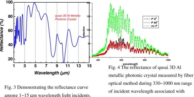
The reflectance spectrum of this device was measured by FTIR and shown as Fig. 3. From this curve, the obvious PBG was found at 3.5 to 7.5 µm regimes [3] and a couple of peaks and valleys among 1 to 3 µm. These behaviors under 1 ~ 3 µm in the reflectivity data is a result of Fabry-Perot type resonance related to the finite thickness of the metallic photonic crystal [11]. These resonances depend on the vertical component of the Bloch-wave vector in the structure and are sensitive to small change in the structure [11]. Note that in the wavelength range down to 1.15 µm (electronic band gap of bulk Si ) Si is
Fig. 2 Top view of qusai 3D MPC sample was observed with SEM instrument after etching away the passivation layer.
fully transparent. For wavelengths below 0.9 µm, the specular reflectivity decreases [11], which can be explained by a combination of diffraction and absorption by the Si in that spectral range.
Further, Cao and Lalanne [12] have argued that surface plasmons (SPs) are most strongly excited near the Wood–Rayleigh anomalies and play a negative role in the transmission anomalies in slit arrays in 2002. Treacy [13] explained the transmission anomalies in terms of a dynamical diffraction theory and indicated that SPs are an intrinsic component of the diffracted wave fields. So mechanisms of the optical transmission of the SP resonant mode (the first transmission peak defined by Porto et al. [14]) though array of slits are not clearly understood and have been a subject of debate.
400 600 800 1000 0 50 100 150 200 re le ct io n wavelength P Oo P 90o no P
Even though, the spectral reflectivity of these finite woodpile crystals can be calculated based on the generalization of the method of ‘‘exact eigenvalues and eigenfunctions’’ used in the study of lamellar gratings [11, 15]. The woodpile structure under consideration can be described as a stack of gratings [11]. In addition, the dip of reflectance around 8.2 µm within the stop band of AL MPC is result from the Carbon-Oxygen single bonds stretching which located in the region of 1200~1100 cm-1 (8.3~9 µm). The bands are generally strong and broad. This CO composition bonds are coming from the low-k dielectric using in 0.18 µm technology node. Similarly, the Si-O-Si oxygen stretching absorption band region is 940~1095 cm-1 (9.1~10.6 µm) which coincides with the second dipping behavior in curve. This silicon oxide bond is the main component of interlayer dielectric in multilayer metal
interconnecting fabrication.
We also observed the reflectance of the sample by fiber optical method at visible region, shown as Fig. 4. From this figure, the obvious grating effect is clear from 400 to 950 nm. The only difference between S and P polarizations is occurred at 550 ~ 620 nm region. This value of wavelength of incident light is almost about the periodic lattice constant of 3D qusai MPC. Therefore, the polarization effect is
1 3 5 7 9 11 13 15 20 40 60 80 100 qusai 3D Al Metallic Photonic Crystal R e fl ect ance ( % ) Wavelength (µµµµm)
Fig. 3 Demonstrating the reflectance curve among 1~15 µm wavelength light incidents.
Fig. 4 The reflectance of qusai 3D Al metallic photonic crystal measured by fiber optical method during 330~1000 nm range of incident wavelength associated with various polarized condition.
bigger while the incident light wavelength is comparable with the lattice constant of MPC. On the other hand, in this structure the polarization effect seems not obvious when the incident light wavelength away from the lattice constant. It means that the reflective light was only influenced by the collective effect of all five layers of Al metal grating.
4. Conclusion
We have made out the qusai 3 dimensional Aluminum metallic photonic crystals (MPC) from the semiconductor manufacture foundry under 180 nm technology node. This sample has shown an obvious PBG effect ranging from 3.5 to 7.5 µm and some other sharp period of transmission region. At the same time, a peculiar performance of grating effect at visible region was demonstrated and
exhibited a little difference during two modes of polarization condition. From this evaluating, we found these samples with certain outline and similar properties. That is no doubt on mass production once qualified MPC parameters being designed.
Acknowledgment
This work is funded and supported by National Science Council under contract 94-2215-E-492-006.
Reference
[1] Lin S Y, Fleming J G, and El-Kady I 2003 Optical Letts. 28 1683 [2] Noda S, 1999 J. Inst. Electron., Inf. Commun. Eng. 82 232 [3] Lin S-Y, Fleming J G, and El-Kady I 2003 Optical Letts. 28 1909 [4] Wijnhoven J E G.J and Vos W L 1998 Science 281 802
[5] Blanco A, et al. 2000 Nature 405 437
[6] Lin S-Y, Fleming J G, Hetherington D L, Smith B K, Biswas R, Ho K M, Sigalas M M, Zubrzycki W, Kurtz S R and Bur J 1998 Nature 394 251
[7] Noda S, Tomoda K, Yamamoto N, and Chutinan A 2000 Science 289 604
[8] Cheng C C, Scherer A, Arbet-Engels V, and Yablonovitch E 1996 J. Vac. Sci. Technol. B 14 4110 [9] E. Ozbay, B. Temelkuran, M. M. Sigalas, G. Tuttle, C. M. Soukoulos, and K. M. Ho 1996 Appl.
Phys. Lett. 69 3797
[10] R. deH¨aen, private communication, 1996
[11] de Dood M J A, Gralak B, Polman A and Fleming J G 2003 Physical Rev. B 67 035322 [12] Cao Q, Lalanne P 2002 Phys. Rev. Lett. 88 403
[13] Treacy M M J 2002 Phys. Rev. B 66, 105
[14] Porto J A, Garc´ıa-Vidal F J and Pendry J B 1999 Phys. Rev. Lett. 83 2845