Resistive switching properties of sol
–gel
derived Mo-doped SrZrO
3
thin films
Chih-Yang Lin
a, Chun-Chieh Lin
a, Chun-Hsing Huang
a, Chen-Hsi Lin
b, Tseung-Yuen Tseng
a,⁎
a
Department of Electronics Engineering and Institute of Electronics, National Chiao Tung University, Hsinchu 300, Taiwan
b
Winbond Electronics Corp., Hsinchu 300, Taiwan Available online 2 August 2007
Abstract
Hysteretic I–V characteristics of the SrZrO3(SZO) thin films with various Mo-doping concentrations were investigated in the study. The
0.2 mol% Mo-doping SZO-based memory device showed excellent resistive switching characteristics, and the resistive switching can be operated over 300 times during successive operation. Both high and low conductive states were stable over 104s. Multi-bit behavior was investigated by dc voltage sweeping with different spans of voltage scan for OFF-process and by various OFF-pulse voltages as well. The endurance test can be over 1000 times with no data loss found. The experimental results showed high potential for nonvolatile memory application.
© 2007 Published by Elsevier B.V.
Keywords: Sol–gel; SrZrO3; Nonvolatile memory; Resistive switching
1. Introduction
With the arrival of digital action life, nonvolatile memory (NVM) plays an important role for portable electrical products, such as mobile phone, digital camera, and notebook. Flash memory is the mainstream among the nonvolatile memory devices nowadays, but it has many drawbacks, including high operation voltage, low operation speed, and poor endurance. In addition, as continuously scaled down, the flash memory faces the challenge of tunneling oxide thinning that causes the unsatisfactory retention time. Consequently, there are many reports and researches for various kinds of nonvolatile memories. Resistance random access memory (RRAM) is one of the promising candidates for the next generation NVM application. Recently, much attention has been paid to development of RRAM devices due to their nonvolatility, simple device structure, and high operation speed[1]. Several research groups reported the experimental results for resistive
switching behavior of Cr-doped SrZrO3 (Cr:SZO) films
epitaxially grown on SrTiO3 (STO) single crystal substrates
by pulsed laser deposition (PLD)[2–4]. The sputtered method
was used for the first time to fabricate the Cr:SZO-based memory device, suggesting that the conduction mechanisms of high and low conductive states are Ohmic conduction and Frenkel-Poole emission, respectively[5]. Further, the resistive switching mechanism from low to high conductive states corresponds to the formation of current paths, and back to low conductive state by the rupture of current paths [6,7]. In this paper, we used the sol–gel method to deposited Mo-doped SZO (Mo:SZO) films to investigate the electrical characteristics. Sol–gel method has the advantages of low cost, easy stoichiometric control, and high uniformity. Various concentra-tions of Mo (0.1, 0.2, and 0.3%) doped SZO thin films were investigated and the possibility for multi-bit storage and the electric-pulse-induce resistance change of the Mo:SZO thin films were also demonstrated for future NVM application. 2. Experimental procedures
First, 150-nm-thick LaNiO3(LNO) conducting films were
deposited on SiO2/Si substrates at 250 °C by a radio-frequency
(rf) magnetron sputter system as the bottom electrodes. The
base pressure of the vacuum chamber was 3.0 × 10− 5 mTorr.
The power density was fixed at 3.3 W/cm2 and constant
working pressure of 10 mTorr which was maintained by a Available online at www.sciencedirect.com
Surface & Coatings Technology 202 (2007) 1319–1322
www.elsevier.com/locate/surfcoat
⁎ Corresponding author. Department of Electronics Engineering and Institute of Electronics, National Chiao Tung University, 1001 Ta-Hsueh Rd., Hsinchu, 300, Taiwan, ROC. Tel.: +886 3 5731879; fax: +886 3 5724361.
E-mail address:[email protected](T.-Y. Tseng).
0257-8972/$ - see front matter © 2007 Published by Elsevier B.V. doi:10.1016/j.surfcoat.2007.07.052
mixture of Ar and O2at a mixing ratio of 3:2 with a total flow of
40 sccm. The deposited LNO film with (100) and (200) preferred orientations was verified by X-ray diffraction (XRD), which was suitable as a template. Then, the LNO films were
annealed by the rapid thermal annealing (RTA) furnace in O2
ambient at 600 °C for 1 min. The SZO thin films with various Mo-doping concentrations, 0.1, 0.2, and 0.3 mol percent, were deposited on LNO bottom electrode by sol–gel method. The stoichiometric amount of the starting materials including strontium acetate (ALDRICH, 99.995%), zirconium n-prop-oxide (ALDRICH 70 wt.% solution in 1-propanol), and mo-lybdenum acetate powder (ALDRICH, 98%), were dissolved in acetic acid (FLUKA, 99.8%) and acetylacetone (FLUKA, 99.5%). Acetic acid was adopted as solvent and heated at 80 °C for 10 min to evaporate the water. Then, the strontium acetate and molybdenum acetate were added into the acetic acid. The mixture was stirred at 80 °C for 30 min to dissolve the solute into the solvent. Subsequently, the acetylacetone and the zirconium n-propoxide were added into the above solution followed by stirred at 80 °C for 60 min to react completely to form the final solution. The prepared 0.1 M precursor solution was spin-coated on the LNO/SiO2/Si substrates to form the sol–
gel film. After baked at 125 °C for 10 min, the as deposited layer was heat-treated at 200 °C for 10 min and then annealed at 400 °C for 30 min. The coating and heating steps were repeated
to obtain the desired film thickness. The thicknesses of Mo:SZO thin films are between 30 and 50 nm based on the observation of cross-sectional scanning electron microscope (SEM). The detailed sol–gel route is summarized in Fig. 1. Finally, a 300-nm-thick Al top electrode with an area of 4.9 × 10− 4 cm2was patterned through a metal mask to form sandwich structure by a thermal evaporator. The current–voltage (I–V) curves were measured by the semiconductor parameter analyzer (Agilent
Fig. 1. Sol–gel route for SZO-based film preparation.
Fig. 2. Schematic view of electrical measurement system.
Fig. 3. XRD patterns of Mo-doped SZO films annealed at various temperatures.
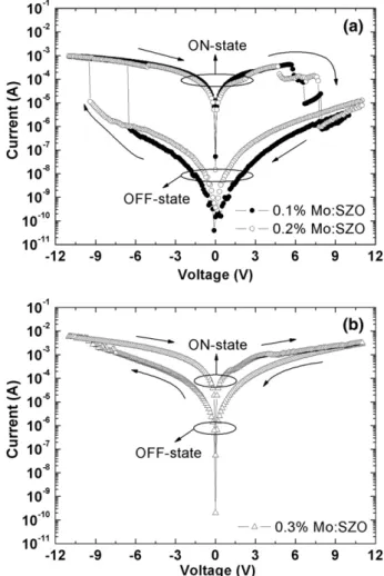
Fig. 4. I–V curves of various 0.1, 0.2, 0.3% Mo-doping SZO-based memory devices.
4155C). The multi-bit storage test and the endurance test of the memory devices were performed by the Agilent 4155C and 81110A. The Agilent 81110A, a pulse/pattern generator, was employed to generate voltage pulses to change the resistance of
the device and the Agilent 4155C was used to measure the leakage current of the device. The schematic view of electrical
measurements system was depicted in Fig. 2and all the
mea-surement were performed at room temperature. 3. Results and discussion
Fig. 3 shows the XRD patterns of the Mo:SZO thin films annealed at various temperatures, indicating that the LNO bottom electrodes have (100) and (200) preferred orientation. Besides, the peaks of SZO (200) thin films appear when the annealing temperature over 600 °C, demonstrating that the SZO thin films are crystallized.Fig. 4depicts the I–V curves of 0.1, 0.2, and 0.3% Mo-doping SZO thin films. While negative voltage is swept on the top electrode to−11V, the current rapidly increases and the device is switched from low conductive state (OFF-state) to high conductive state (ON-state). The state holds
on ON-state after sweeping the bias voltage from−11 to 0 V.
Subsequently, the bias voltage sweeps to positive and changes the device from ON-state to OFF-state after passing a transition region, showing the negative differential resistance (NDR), and the OFF-state is hold as sweeping back to 0 V. The resistance
ratio between ON- and OFF-state is over 103when the doping
concentrations of Mo are 0.1 and 0.2%. Moreover, the resistive switching behavior of the 0.2% Mo-doping SZO shows more reliable than that with 0.1% Mo-doping. The resistive switching behavior of the SZO memory film becomes worse for 0.3% of
Mo-doping SZO as shownFig. 4(b).
According to previous reports, Sawa et al. proposed a model of Schottky barrier altered by trapped charge carriers in the
interface, causing the resistance changed [8]. Chen et al.
suggested that small changes in oxygen concentration may result in large resistance change and the oxygen stoichiometry change induced by electric field might not be uniformly distributed in the interface region[9]. Lin et al. proposed that in the ON-process, the biased electrons found one or few conducting paths composed of possible point defects including oxygen vacancies, ionic, and electronic defects, and the OFF-process was caused by the defects would trapped electrons, thus
Fig. 7. Multi-bit storage test performed by different OFF-pulses with fixed ON-pulse.
Fig. 5. (a) The 1st, 10th, and 300th, I–V curves during successive resistive switching of the Al/0.2%–Mo:SZO/LNO device. (b) plot of current versus time for the device.
Fig. 6. The hysteretic I–V characteristics of the Al/0.2%–Mo:SZO/LNO device measured with different spans of voltage scan for OFF-process.
1321 C.-Y. Lin et al. / Surface & Coatings Technology 202 (2007) 1319–1322
leading to the rupture of conducting paths[6]. In our study, we assumed that the resistive switching behavior in the Al/0.2%– Mo:SZO/LNO device is due to the formation and rupture of conducting paths, where composed of various kinds of defects. The appropriate dopant species and concentration are used to control the defects within the SZO thin films[10,11]. Besides, the interface reaction between electrodes and SZO thin films might also influence the resistive switching characteristics[12]. However, the detailed resistive switching mechanism is still unclear, and further study is needed for elucidating the origin of the resistive switching mechanism and the doping effects.
The 1st, 10th, and 300th, I–V curves during successive resistive switching of the Al/0.2%–Mo:SZO/LNO device are
shown in Fig. 5(a), indicating the device can perform the
resistive switching up to 300 times.Fig. 5(b) demonstrates the
nondestructive readout property in the Al/0.2%–Mo:SZO/LNO
device and both ON- and OFF-state stressed at 0.5 V are very stable over 104s.
Due to the NDR phenomenon presented during OFF-process, the hysteretic I–V characteristics of the Al/0.2%–Mo:SZO/LNO device were investigated with different spans of voltage scan
for OFF-process. Bias voltage was swept as 0 V→−4 V (current
limited at 0.1A)→0 V→1 V (VOFF-1)→0 V→2.5 V (VOFF-2)
→0 V→5 V (VOFF-3)→0 V. As the VOFFincreased, the higher
resistance value of OFF-state increased, which demonstrating the possibility for multi-bit storage application and the result was shown inFig. 6. To further investigate this electrical property, different positive voltages with 5, 7, and 9 V were applied to switch the device into various OFF-states, while switching the device into ON-state was fixed at−5 V as shown in the inset of Fig. 7. All the pulse widths used here were 10 ns. The multi-bit storage was well demonstrated by various positive voltage pulses as shown inFig. 7.
The electrical-pulse-induced resistance change (EPIR)
property was performed by applying a −2 V, 10 ns voltage
pulse to switch the state into ON-state, and back into OFF-state
again by 5 V, 10 ns voltage pulse. The endurance test can be
operated over 1000 times as shown inFig. 8. Due to the EPIR
property, the Al/0.2%–Mo:SZO/LNO device shows high potential for future NVM application.
4. Conclusions
Resistive switching properties of various Mo-doping con-centrations SZO films were investigated in the study. The SZO-based memory device with 0.1 and 0.2% mole Mo-doping showed better resistive switching characteristics than that with 0.3%. The resistive switching of the Al/0.2%–Mo:SZO/LNO device can be operated over 300 times during successive operation. The nondestructive readout test of both ON- and OFF-state was stable over 104s. Multi-bit application of the Al/ 0.2%–Mo:SZO/LNO was investigated by dc voltage sweeping with different spans of voltage scan for OFF-process. As the
VOFF increased, the higher resistance value of OFF-state
increased. The different OFF-states were also obtained by various OFF-pulse voltages with fixed ON-pulse voltage. The endurance test would be over 1000 times with no data loss found. The Al/0.2%–Mo:SZO/LNO device shows high poten-tial for nonvolatile memory application.
Acknowledgement
This work was supported by the Winbond Electronics Corporation, Taiwan, and by the National Science Council, Taiwan, under project NSC 95-2221-E009-278.
References
[1] W.W. Zhuang, W. Pan, D.B. Ulrich, J.J. Lee, L. Stecker, A. Burmaster, D.R. Evans, S.T. Hsu, M. Tajiri, A. Shimaoka, K. Inoue, T. Naka, N. Awaya, K. Sakiyama, Y. Wang, S.Q. Liu, N.J. Wu, A. Ignatiev, Int. Electron Devices Meet. Tech. Dig. (2002) 193.
[2] A. Beck, J.G. Bednorz, Ch. Gerber, C. Rossel, D. Widmer, Appl. Phys. Lett. 77 (2000) 139.
[3] Y. Watanabe, J.G. Bednorz, A. Bietsch, Ch. Gerber, D. Widmer, A. Beck, S.J. Wind, Appl. Pyhs. Lett. 78 (2001) 3738.
[4] C. Rossel, G.I. Meijer, D. Bremaud, D. Widmer, J. Appl. Phys. 90 (2001) 2892.
[5] C.-Y. Liu, P.-H. Wu, A. Wang, W.-Y. Jang, J.-C. Young, K.-Y. Chiu, T.Y. Tseng, IEEE Electron Device Lett. 26 (2005) 351.
[6] C.C. Lin, B.C. Tu, C.C. Lin, C.H. Lin, T.Y. Tseng, IEEE Electron Device Lett. 27 (2006) 725.
[7] J.-W. Park, K. Jung, M.K. Yang, J.-K. Lee, D.-Y. Kim, J.-W. Park, J. Appl. Phys. 99 (2006) 124102.
[8] A. Sawa, T. Fujii, M. Kawasaki, Y. Tokura, Appl. Phys. Lett. 85 (2004) 4073.
[9] X. Chen, N. Wu, J. Strozier, A. Ignatiev, Appl. Phys. Lett. 89 (2006) 063507.
[10] Y.P. Wang, T.Y. Tseng, J. Appl. Pyhs. 81 (1997) 6762.
[11] C.-F. Chung, J.-P. Lin, J.-M. Wu, Appl. Phys. Lett. 88 (2006) 24909. [12] T.-N. Fang, S. Kaza, S. Haddad, A. Chen, Y.-C. Wu, Z. Lan, S. Avanzino,
D. Liao, C. Gopalan, S. Choi, S. Mahdavi, M. Buynoski, Y. Lin, C. Marrian, C. Bill, M. VanBuskirk, M. Taguchi, Int. Electron Devices Meet. Tech. Dig. (2006) 789.
Fig. 8. Endurance test over 100 times by voltage pulses.