指導教授:趙天生 博士
研 究 生:吳立盈
中華民國 一百零一 年 九 月
國 立 交 通 大 學
電子物理研究所
碩士論文
鍺基紅外光偵測器應用於光連接系統之
設計與建模
Design and modeling of Germanium based Photodetectors for
on-chip optical interconnects
鍺基紅外光偵測器應用於光連接系統之
設計與建模
Design and modeling of Germanium based Photodetectors
for on-chip optical interconnects
國立交通大學
電子物理所碩士班
碩士論文
Institute of Electrophysics
National Chiao Tung University
A Thesis Submitted to Department of Electronphysics College of
Science National Chiao Tung University in Partial Fulfillment of the
Requirements for the Degree of Master of Science in Electrophysics.
September 2012,
Hsinchu, Taiwan, Republic of China.
中華民國 一百零一 年 九 月
指導教授 :趙天生 博士 Advisor : Dr. Tien-Sheng Chao
Abstract
As one of the crucial components in optical interconnect system, germanium photodiodes (GePD) are promising due to its corresponding bandgap (0.66 eV) to absorb infra‐red light and the compatibility to silicon‐based photonics and electronics. However, many researchers have shown that the key issue of GePD is high dark current, and efforts were done to suppress the dark current and to increase gain‐bandwidth product by improving GePD efficiency and speed. This thesis aims to systematically find the photo‐electrical behavior based on the simplest P‐i‐ N germanium photodiodes. To investigate the main physical mechanism behind the dark current of germanium photodiode, analysis of temperature dependence ofexperimentally measured dark current is performed. After that, several guidelines toward the GePD structure are provided in this thesis with the aid of TCAD simulation, which can be a useful reference when fabricating high‐efficiency and low‐power consumption germanium photodetector with lateral P‐i‐N structure.
摘要
在取代積體電路銅導線的光連接傳輸系統中,紅外光偵測器是光學訊號接收端的重要
元件,其中,鍺的能隙(0.66 eV) 使得鍺基元件能夠有效吸收紅外光訊號,鍺基紅外
光偵測器近年來成為許多研究的題目。文獻指出,鍺基紅外光偵測器的主要缺點是暗
電流過高,造成訊號干擾以及額外功率消耗。本篇論文以水平 P-i-N 結構的鍺基紅外
光偵測器為研究對象,首先透過變溫量測與分析,得知在室溫以及小偏壓操作下,暗
電流來自於 Shockley-Read-Hall 載子產生過程 (SRH generation)。接著利用 TCAD 模
擬軟體,取用上述 SRH 模型,模擬不同幾何參數對於偵測器之暗電流、光電流以及傳
輸速度的影響,探討各參數的權衡與最佳化,為未來提供製造低雜訊、高效率以及高
頻寬的鍺基紅外光偵測器的方針。
Foreword
I’d like to acknowledge the contribution of two persons to this thesis. One is Prof. Marc Heyns, the thesis supervisor, whose advisement enables this thesis more physically logical. One is Dr. Geert Hellings, my daily supervisor; I deeply appreciate him for his generous teaching, continued guidance, and endless patience.
I am also grateful to members in KULeuven University and National Chiao‐Tung University who are in charge of the dual‐degree Master program, which provided me such a wonderful opportunity to study here. For the two‐year research days in Taiwan, I’d like to acknowledge Prof. Tien‐Sheng Chao, who is not only an encouraging teacher but also a supporting mentor. In the free and respectful research environment he provides, I am lucky to meet all the members in the Advanced Semiconductor Device Fabrication and Measurement Lab, and the times we spent together studying and doing experiments in the clean room are definitely memorable.
Finally a big thank you goes to my dear family, wherever in Taiwan or Belgium, I never stop feeling their immediate love and support.
Li‐Ying Wu
Table of Contents
Abstract ... v摘要 ... vii
Foreword ... ix
Table of Contents ... xi
List of figures and tables ... xiii
List of figures ... xiii
List of Tables ... xv
Chapter 1
Introduction... 1
1.1 Optical Interconnect: A System Overview ... 1
1.1.1 History ... 1
1.1.2 Photodiodes in optical interconnect system ... 2
1.2 Working principle of P‐i‐NGePD ... 3
Chapter 2
Experimental Investigation of Dark Current in Germanium photodiodes ... 5
2.1 Dark Current Mechanisms in Ge Photodiode ... 5
2.1.1 Diffusion Currents ... 5
2.1.2 SRH current ... 7
2.1.3 Tunneling and Impact Ionization ... 9
2.2 Measurements of Germanium photodiodes ... 10
2.2.1 Structure of GePD ... 10
2.2.2 Temperature dependence measurement ... 11
2.3 Temperature Dependence of dark current ... 13
2.4 Conclusion ... 19
Chapter 3
Dark Current in Germanium photodiodes: TCAD simulation ... 21
3.1 TCAD Models ... 21
3.1.1Default Models in TCAD (including Diffusion) ... 21
3.1.2 SRH: The Shockley‐Read‐Hall Model... 21
3.2 Base structure formed in TCAD ... 22
3.3TCAD Optimization of Dark Current ... 26
3.3.1 Alterations in thickness ... 26
3.3.2 Alterations in width ... 29
3.3.3 Alterations in implant energy ... 32
3.4 Conclusion ... 33
Chapter 4
Quantum Efficiency Optimization ... 35
4.1 Optical Generation and definition of Quantum Efficiency ... 35
4.1.1 Optical Generation Method ... 35
4.1.2 Definition of Quantum Efficiency (QE)... 37
4.2 QE in respect of Structural parameters ... 38
4.2.1 QE dependence on thickness and width of GePD ... 38
4.2.2 QE dependence on doping separation ... 40
4.3 QE improvement by Junction engineering ... 42
4.4 Conclusion ... 44
Chapter 5
Transient Response Optimization ... 45
5.1 The Role of Transient Response ... 45
5.2Speed in respect of structural parameters ... 47
5.3 Length effect ... 50
5.3.1 Capacitance in length direction ... 50
5.3.2 Absorption in length direction ... 51
5.4 Frequency response ... 53
5.4.1 Bit stream input ... 53
5.4.2 Eye diagram ... 53
5.5 Conclusion ... 55
Chapter 6
Conclusion ... 57
Appendices ... 61
Appendix A: Command codes in TCAD simulator ... 63
Sprocess ... 63
Sdevice for IV ... 67
Sdevice for C‐V ... 70
Sdevice for transient ... 72
Bibliography ... 75
List of figures and tables
List of figures
Fig. 1‐1 System overview of optical interconnection[4]. ... 2Fig. 1‐2Illustration and band diagram of a lateral PiN GePD in reverse bias. ... 3
Fig. 2‐1 Energy band diagram of p‐n junction in reverse bias. ... 6
Fig. 2‐2 Shockley‐Read‐Hall generation process[9]. ... 7
Fig. 2‐3 Band diagram and tunneling process of heavily doped diodes[9][15]. ... 9
Fig. 2‐4 Structure of germanium photodiode. ... 10
Fig. 2‐5 Large distribution of dark current vs. Length of GePD. ... 12
Fig. 2‐6 Temperature dependence of I‐V characteristics (with parasitic leakage)... 12
Fig. 2‐7 Temperature dependence of I‐V characteristics. ... 13
Fig. 2‐8 Activation energy versus reverse bias from experimental data. ... 14
Fig. 2‐9 Reverse Currents (A/µm) versus 1000/T(K‐1). ... 16
Fig. 2‐10 Total reverse current subtracted by diffusion current. ... 17
Fig. 2‐11 Variation of recombination lifetime versus effective dopant concentration[18]. ... 18
Fig. 3‐1 Simulated structure of germanium photodiode in TCAD, showing dopant profiles, meshing. ... 22
Fig. 3‐2 Simulated structure with exponential (top) and constant (bottom) defect distribution profile. ... 23
Fig. 3‐3 Dark current experiment data and results of Exponential defect profile (Top) simulation and constant defect profile (bottom) simulation. ... 24
Fig. 3‐4 Defect determined forward swing behavior indicated accuracy of the defect density level acquired from simulation of dark current. ... 25
Fig. 3‐5 Simulated dark current as a function of Total Ge thickness. ... 27
Fig. 3‐6 Trap number comparison between constant and exponential defects. ... 28
Fig. 3‐7 Effects of the width of germanium on dark current. ... 29
Fig. 3‐8Dark current of different diodes versus doping separation ratio. ... 30
Fig. 3‐9 Electric field distribution in diodes with different doping separation. ... 31
Fig. 3‐10 Dark current versus implant energy ratio. ... 32
Fig. 3‐11 Electric field distribution of diodes with different junction depth ... 32
Fig. 4‐1 The 2Dsingle‐modeinfrared light intensity distribution inside a 2D Germanium structure of 2‐μm‐wide and 0.2‐μm‐thick. ... 35
Fig. 4‐2 Two‐dim Gaussian optical signal in the TCAD simulator. ... 36
Fig. 4‐3
Light distribution in photodiodes with different width and thickness. ... 38
Fig. 4‐4 Effects of Ge thickness and width on QE. ... 39
Fig. 4‐5 QE dependence on doping separation. ... 41
Fig. 4‐6Dark current and QE as a function of implant energy. ... 42
Fig. 4‐7 Deep junctions and shallow junctions. ... 43
Fig. 4‐8 Effects of deep‐and‐shallow junctions on dark current and QE. ... 43
Fig. 4‐9 The optimum structure for low dark current and high QE. ... 44
Fig. 5‐1 Illustration of rise time definition... 45
Fig. 5‐2 Effective circuit of a PIN photodiode[20][21]... 46
Fig. 5‐3 C‐V characteristics of simulated photodiode with various structures. ... 48
Fig. 5‐4 Speed of GePD is inversely proportional to wGe. ... 48
Fig. 5‐5.Speed evaluation of GePDs with different Wi and wGe. ... 49
Fig. 5‐6Parasitic Capacitance CPDobtained with length of GePD. ... 50
Fig. 5‐7 Optical absorption coefficient of Si, Ge, and SiGe alloys[22]. ... 51
Fig. 5‐8 Absorption ratio versus length of germanium photodiode. ... 52
Fig. 5‐9 The bit stream input contains combinations three bits. ... 53
Fig. 5‐10 Eye diagram of the GePD with speed 30GHz. ... 54
List of Tables
Table 2‐1 Structural parameters of GePD. ... 11 Table 6‐1 Several Guidelines for designing GePD. ... 59 Table 6‐2 GePD equivalent circuit [19] [20]and acquired value of components. ... 60
Chapter 1
Introduction
The objective of this thesis is to find an optimum structure of the germanium photodiode inside the optical interconnect system. To start, a system overview of optical interconnect is introduced, and the working principal of a photodiode is given.
1.1 Optical Interconnect: A System Overview
1.1.1 History
Information processing relies on linear and non‐linear devices and circuits for logic and storage functions, and also requires interconnections to carry the signal from one place to another. As the counting reduction in feature sizes on electronic chips leads to a larger numbers of faster devices at lower cost per device, the scaling of electrical interconnections doesn’t keep up with the growth of electrical devices. The traffic in long‐distance is limited by various problems of electrical wiring, for example, high resistance and high parasitic capacitance of long wires. This degrades the speed improvement via devices researches, and global interconnects will become very difficult if people keep using conventional method[1].
The research for optical interconnects starting as early as semiconductor diode laser had been invented, and the first idea that optical interconnects can be utilized in very‐large scale‐integration (VLSI) was proposed and analyzed by Goodman, et al. in 1984. Same year, the quantum confined Stark effect was discovered in III‐V semiconductor quantum wells, which enables efficient high‐speed optical modulators. Integrated waveguide versions of such modulators are extensively today for high‐performance applications[2].
The advantages of using optical interconnects makes development attractive, such as less distance dependency on performance, ability to have 2‐D interconnects rather than connect from edge, and feasibility of wavelength division multiplexed interconnects without using any electrical multiplexing circuitry. More details were enumerated in literatures[1][3].
1.1.2 Photodiodes in optical interconnect system
Optical interconnects require the integration of various technologies. Fig. 1‐1 shows the overview of a simple set of photonic transceiver and receiver [4], where electrical‐optical signal transition happens. Left‐hand side of Fig. 1‐1 is a silicon modulator consists of optical ring resonators. The modulator takes electrical signals and monochromic laser lights as inputs and generates optical signals of infrared frequency as optical data, which then passages through a silicon waveguide routed on the chip and arrives at the destination chip. At right‐hand side, a germanium photodetector is there to capture transmitted optical data, and then transfer optical signals into pulses of electrical currents. Fig. 1‐1 System overview of optical interconnection[4].
As one of the crucial components in optical interconnect system, germanium photodetectors, or Germanium photodiodes (GePDs), have been broadly investigated due to its corresponding bandgap to absorb infrared light at 1.55‐μm wavelength and the compatibility to silicon‐based photonics and electronics. GePDs monolithically integrated with silicon transistor technology is viewed as the essential part of infrared optical interconnects system.
However, many researchers have shown that the issue technology issue of GePD is high dark current, due to the 4.2% mismatch between Ge and Si, and efforts were done to suppress the dark current by means of improving fabrication process [5][6]
To improve GePD efficiency and speed, advanced GePD are developed to increase the photocurrent in regular P‐i‐N GePD by utilizing multiplication of carriers, for example, Avalanche photodetector (APD) and separate‐absorption‐charge‐ multiplication (SACM) photodiode [7]. Literature [8] proposed that creation of non‐ uniform electric field in germanium APD via nanoelectric engineering increases the gain‐bandwidth product.
The purpose of this thesis is to systematically find the photo‐electrical behavior based on the simplest P‐i‐N germanium photodiodes but with various structural parameters, with the aid of TCAD simulator; so that a basic guideline can be provided for the future advanced researches. In next section, working principles of P‐i‐N
1.2 Working principle of P‐i‐N GePD
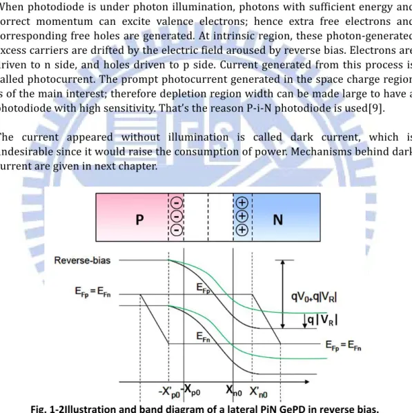
Fig. 1‐2 shows the illustration and the band diagram of a lateral P‐i‐N GePD in reverse bias. Green lines represent the conduction and valence band edge at equilibrium, and distance between ‐Xp0 and Xn0 represent the depletion width at
equilibrium. When a reverse bias is applied, depletion retrieves away from the center of diode (to –X’p0 and X’n0), and the exposed ionized dopants provide extra electric
fields, which can be seen from the increasing slope of band edges.
When photodiode is under photon illumination, photons with sufficient energy and correct momentum can excite valence electrons; hence extra free electrons and corresponding free holes are generated. At intrinsic region, these photon‐generated excess carriers are drifted by the electric field aroused by reverse bias. Electrons are driven to n side, and holes driven to p side. Current generated from this process is called photocurrent. The prompt photocurrent generated in the space charge region is of the main interest; therefore depletion region width can be made large to have a photodiode with high sensitivity. That’s the reason P‐i‐N photodiode is used[9].
The current appeared without illumination is called dark current, which is undesirable since it would raise the consumption of power. Mechanisms behind dark current are given in next chapter. Fig. 1‐2Illustration and band diagram of a lateral PiN GePD in reverse bias. In the following chapters, operation conditions are all considered under a reverse bias of absolute value 0.5 volt, and for short sometimes it is put as
‐
0.5V.Chapter 2
Experimental
Investigation of Dark Current in
Germanium photodiodes
In this chapter, dark currents mechanisms are enumerated. Next, the results of temperature dependence measurement of GePD dark currents and the analysis are presented.
2.1 Dark Current Mechanisms in Ge Photodiode
To start with, several components of photodiode dark current which result from different mechanisms are considered before analysis. They are respectively diffusion current, thermal generation current, tunneling current and impact ionization current[10].
A well‐performed photodiode needs to keep its dark current low enough, to avoid high power consumption at stand‐by stage and even noise when light signals turned on. Compared to silicon devices, germanium diode is more likely to be suffered from higher junction leakage due to its small band gap (0.66 eV). What’s more, high dark current leakage is the critical issue in Ge PDs technology as compared with III‐V based photodiodes. Therefore, clarifying of the main recombination mechanisms is indispensable for of Ge photodiode electrical behavior simulation, and further for Ge photodiode optimization. In this chapter, the physical mechanisms behind dark current are viewed, and the experimental investigation of dark current is performed.
2.1.1 Diffusion Currents
Diffusion current is proportional to the gradient of the carrier concentration evaluated at the interface between the depletion and the neutral region[11]. Energy band diagram of a p‐n junction in reverse bias is shown as Fig. 2‐1. For example, in p‐ type quasi‐neutral region areas, the equilibrium minority or electron concentration np0 is: Eq. 2‐1 where NA is acceptor concentration in p‐type region. Those electrons would diffuse
1 Eq. 2‐2 Eq. 2‐3 Since ni is positively correlated to temperature, we can tell from Eq. 2‐3 that diffusion current would increases when rising temperature with an activation energy equals to the band gap of germanium [12]. Fig. 2‐1 Energy band diagram of p‐n junction in reverse bias.
2.1.2 SRH current
Besides diffusion current, recombination‐generation current should also be concerned. Since basically photodiode operates in ‐0.5 volts, under this reverse condition, the electric field in depletion region sweeps holes to the p‐type region and electrons to n‐type region. Because of the reduction in carrier concentration (np « ni2), system is prone to generate more carriers to meet equilibrium.
Many researchers have found dark current is greatly depends on the quality of junction layers. This indicates that the generation process involves impurities or imperfections. Those imperfections disrupt the lattice of semiconductor and introduce energy levels into the band‐gap. In our case, most of the imperfections come from dislocations at the interface of silicon waveguide and germanium layer due to lattice mismatch. Fig. 2‐2illustrates this generation process, or so‐called Shockley‐Read‐Hall recombination.
Fig. 2‐2 Shockley‐Read‐Hall generation process[9].
The net generation‐recombination rate, U, of carriers through these intermediate centers has been successfully described by Hall, Shockley and by Read[13][14]. It can be shown that:
U σ σ v pn n N
σ n n exp σ p n exp Eq. 2‐4
where σp and σn are the capture cross‐sections for holes and electrons respectively,
vth is the thermal velocity, n is the electron concentration, p is the hole concentration,
Nt is the concentration of bulk generation‐recombination centers at the energy level
Et, Ei is the intrinsic Fermi level and ni the intrinsic carrier concentration.
To summarize, components of diffusion and thermal generation currents in a p‐n junction could be described as following equation [Sze, sensor]
∙ Eq. 2‐5
where q is elementary charge, Dn is the electron diffusivity, τn is the electron life time,
NA is the doping level of the p‐type region, ni is the intrinsic concentration of
semiconductor, in this case, germanium, τgen is the generation lifetime, and W is the
depletion width. A similar expression holds for holes.
The second term of Eq. 2‐5 states SRH recombination/generation current is dependent on carrier life time τgen; namely, this source of dark current is influenced
by the number of defects that served as recombination/generation sites[12]
More details will be discussed in section 2.3, while analysis of germanium dark current under different temperature and reverse bias based on experimental measurement is presented.
2.1.3 Tunneling and Impact Ionization
In a diode with degenerately doped p‐n junctions, tunneling can be determining when reverse bias is above a certain value, since depletion region is relatively narrow in highly doped diodes and hence smaller tunneling barrier. The process is shown in Fig. 2‐3. Tunneling current could be band‐to‐band tunneling (BTBT) and trap‐ assisted tunneling (TAT).
Fig. 2‐3 Band diagram and tunneling process of heavily doped diodes[9][15].
At higher applied voltages, impact ionization plays a role followed by avalanche breakdown. The avalanche breakdown process occurs when carriers moving across the space charge region, acquire sufficient energy from the electric field to create electron‐hole pairs by colliding with atomic electrons within the depletion region[9]. Analytical model describing reverse characteristics of a p‐n diode including tunneling current and avalanche breakdown was presented in [16].
However, in this thesis, the structure we discussed is a P‐i‐N junction, whose intrinsic width is at least 0.5 µm. With this sufficient large tunneling barrier, and the operation condition that only under low electric field, it’s reasonable to conclude that tunneling current and impact ionization currents are negligible.
2.2 Measurements of Germanium photodiodes
2.2.1 Structure of GePD
The structure GePD device used in this thesis looks like Fig. 2‐4,in Fig. 2‐4(bottom), silicon layer serves as an optical signal waveguide; it is recessed into trapezoidal shape by etch‐back process, and from Fig. 2‐4(right) we can see this trapezoidal shape is formed the (111), (113) and (100) facets of silicon. The taper angle (see (bottom)) is approximately 30°, which is used to increase the coupling efficiency for light to transmit through Si/Ge interface[17]. Lying on top of the silicon is the main body of photodetector, formed by germanium selective epitaxial growth. After annealing and CMP process, boron and phosphorus implantation is applied to form P+ and N+ side respectively, and after the process of oxide layer deposition and contact‐hole formation, tungsten electrodes are filled in. The cross‐section of GePD resembles a mushroom, and the “cap” of mushroom is called overlap region. Overlap region is designed to separate tungsten electrodes far away from light intensity, so that light intensity loss from metal absorption can be decreased. All the meanings of structural parameters are listed in Table 2‐1.
Fig. 2‐4 Structure of germanium photodiode.
(left)Top view of GePD; (right)TEM structure of GePD; (bottom) GePD Structure illustration with parameters
Terms Meanings hGe Total thickness of Germanium diode (=hov+hBody+hRec) hBody Thickness of Germanium body hov Thickness of overlap hRec Recession depth (= Si etched‐back thickness) wGe Width of Germanium diode Wi Doping separation; Width of intrinsic region θ Tapered angle formed when silicon etch‐back process tSi Thickness of silicon Table 2‐1 Structural parameters of GePD.
2.2.2 Temperature dependence measurement
To analyze dark current behavior, a series measurement of the current‐voltage characteristic with varying temperature has been done. The temperature dependence measurement is performed by HP4156 Semiconductor Parameter Analyzer. Fig. 2‐6shows the I‐V characteristics of photodiode measured under different temperature from ‐10°C to 125°C, sweeping anode (connect to P+ terminal
of GePD) voltage from ‐2V to 1V.
However in Fig. 2‐6, sets of curves is merging together as arrowed, which means that dark currents are interfered by exterior leakage path, for example, leakages that come along the edge of germanium. Furthermore, this parasitic current is difficult to be normalized with length because as we measured the leakage currents of diodes with 10, 20 and 50μmlongand there is no correlation between current and length. A large distribution is shown in Fig. 2‐5.This phenomenon is also diverse from sample to sample throughout the whole wafer.
It is more meaningful to analyze the intrinsic behavior of leakage currents in germanium photodiode; after a series of “searching for the best die,” measurement data that worthy discussing is put in the 2.3 section.
Fig. 2‐5 Large distribution of dark current vs. Length of GePD. Large distribution prevents accurate extract of dark current. Fig. 2‐6 Temperature dependence of I‐V characteristics (with parasitic leakage).
2.3 Temperature Dependence of dark current
The result of measuring “the best die” is shown in Fig. 2‐7, in which curves are more smooth compared to those interfered by parasitic leakages. And then, activation energy is estimated based on Arrhenius equation (Eq. 2‐6) by fitting data with exponential function in the plotting of measured dark current at a given reverse bias versus 1/T (not shown), and extracting the exponent to calculate activation energy Ea at each reverse bias point. Fig. 2‐7 Temperature dependence of I‐V characteristics.
Activation energy is the energy needed for electrons to overcome process barrier. The activation energy for diffusion process is germanium bandgap 0.66 eV, and for SRH process with deep traps Ea should be close to half bandgap, 0.33 eV. Activation energy versus reverse bias is shown in Fig. 2‐8.
k
Ae
/Eq. 2‐6
Fig. 2‐8 Activation energy versus reverse bias from experimental data.
Dark current is initially dominated by diffusion mechanism near zero volts, and continually Shockley‐Read‐Hall generation takes place in higher reverse bias.
Ea of five samples as a function of reverse bias are shown in Fig. 2‐8.Only the top curve (red solid triangles) maintains above Ge half bandgap (0.33 eV) until ‐2V, which is regarded behaving as intrinsic semiconductor leakage. Other four curves (small dots) reveal that these samples are more affected by leakages from parasitic conducting path.
Activation energy is dropping as reverse bias increases (goes to negative/left direction as arrowed). For the top curve, it starts with Ea ≈ 0.6 eV, which means that the average dark current over ‐10°C to 125°C is dominated by diffusion of minority carriers in small bias. As reverse bias gets higher, Ea gradually drops close to 0.3 eV, which means that at higher reverse bias, average dark current is subjected to SRH recombination process.
Another analysis shows this trend similarly. In Fig. 2‐9, the logarithm of the measured leakage current (curves with blue solid symbols) at different applied voltages are plotted versus 1000/T together with ni and ni² dependencies (straight lines with open symbols). The inset of Fig. 2‐9 is again Eq. 2‐5, with first term related to diffusion current and second term related to SRH generation current as indicated.
ni dependency on temperature is shown more clearly in Eq. 2‐7. Bandgap correction
with respect to temperature is taken into account when plotting of ni and ni² dependencies. 2 2 2 ∗ 2 2 ∗ 2 Eq. 2‐7
In Fig. 2‐9, it shows that SRH generation leakage has a stronger dependence on reverse bias compared to diffusion current. It is because with higher reverse bias, the diode is more depleted (depletion region gets wider), which means more traps are exposed out as generation sites, resulting in higher generation current. Sets of curves show a trend that dark current of measured GePD is in a combination behavior of diffusion and SRH generation. Judged from the slope and tangent line, SRH generation is the main component in dark current at room temperature 25°C, while the GePD is at its operation point ‐0.5V. Above 87°C, diffusion current plays a role.
Fig. 2‐10demonstrates this more clearly, which is the zoom in version of Fig. 2‐9, while Y‐axis is replaced as the amount of measured current subtracted by calculated diffusion current (first term of Eq. 2‐5), which should give SRH generation behavior. A neat fitting with SRH equation lines (five parallel yellow lines) could be seen in temperature below 25°C. Deviations in higher temperature and higher reverse voltage regime are supposed to attribute to extra current from diode edge, which is randomly distributed as shown before.
Fig. 2‐9 Reverse Currents (A/µm) versus 1000/T(K‐1).
Measured current (solid symbols) at different temperature as a function of 1000/T. Two straight lines with open symbols are plotted from Eq. 2‐5 as in the inset, with first term related to diffusion current and second term related to SRH generation current as indicated.
Fig. 2‐10 Total reverse current subtracted by diffusion current. Solid symbols are measured total current subtracted by pure calibrated diffusion current from Eq. 2‐5, and empty symbols are pure calibrated Shockley‐Read‐Hall current from equation.
Lifetimes of electrons are also roughly calculated to be 0.06 µs. Based on literature[18], the defect density of the best die is estimated around 1e19/cm3 from
Fig. 2‐11 Variation of recombination lifetime versus effective dopant concentration[18].
2.4 Conclusion
At the beginning of this chapter, we overviewed physical mechanisms behind dark current in a germanium photodiode. Section 2.2 describes the structure of germanium photodiode used in this thesis, and the temperature dependence measurement method. Severe parasitic leakage was observed on many devices. Due to this yield issue, a meaningful analysis could only be performed on well‐chosen devices.
Subsequently, in section 2.3, we show the investigation of dark current in germanium photodiode via experimental data.
Firstly, from the analysis of activation energy, when the bias is small, the average dark current over ‐10°C to 125°C is diffusion current; as bias gets more reversed, it would subject to SRH process. Secondly, it can be verified that dark current is in the combination behavior of diffusion current and SRH generation current. At room temperature, and at the bias ‐0.5V, SRH generation is the main component in dark current. There is a good qualitative agreement between formula trend and measured data. Thirdly, from a rough estimate of carrier lifetime, equivalent trap densities of our best samples are estimated to be around 1E19/cm3.This will be more precisely
estimated in Chap 3.
Chapter 3
Dark Current in
Germanium photodiodes: TCAD
simulation
In the previous chapter we concluded that diffusion and SRH generation current are mainly the leakage sources of germanium photodiode. In this chapter, TCAD simulation is involved. This chapter starts with an overview of models that are used in our simulation, and the base structure we build in TCAD, finally we make alteration in the base structure and show an optimum structure that has minimum dark current.
3.1 TCAD Models
3.1.1Default Models in TCAD (including Diffusion)
Physical models used to simulate germanium photodiode are presented. Diffusion current can be treated as the intrinsic behavior of semiconductor. It is standardly activated in the TCAD simulator.
3.1.2 SRH: The Shockley‐Read‐Hall Model
As mentioned in Chapter 2, SRH model describes recombination/generation through deep‐level defects in the semiconductor bandgap. The position of the dominating trap level in the bandgap is assumed at midgap energy level (0.33 eV) for Ge[19]. Basically, an expression of SRH is used in terms of minority carrier lifetimes (τn and
τp), dependent on the local defect concentration.
3.2 Base structure formed in TCAD
The ultimate purpose of this thesis is to find an optimized structure of germanium photodiode through simulation, so it is important to get a base structure which is close to the measured diode, including similar geometry and effective defect density, and then we can utilize this base structure to simulate the currents of photodiodes with alteration. The inclusion of TCAD enables us to get the approximate form of defect density in the measured samples.
To form a base structure, the fabrication flow which is identical to experimental samples is simulated via TCAD sprocess tool, and the final simulated structure is shown in Fig. 3‐1. Contacts are simulated as ideal ohmic contact, and in Fig. 3‐1 they are shown in boundary only. Note that simulations are done in a two‐dimensional GePD, so the current from electrical characteristic simulation is given by Ampere per µm (A/µm). That is, in simulation, the length of germanium (LGe) is always considered as 1 µm, only in Section 5.2 we would alter LGe to see the effects happen in length direction. Fig. 3‐1 Simulated structure of germanium photodiode in TCAD, showing dopant profiles, meshing.
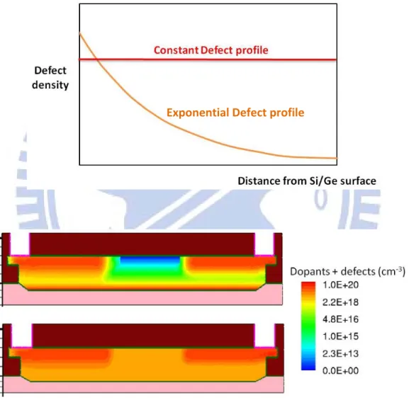
In order to estimate the defect density inside germanium photodiodes, a constant defect distribution is introduced into simulator. That is, we build up a simulated germanium photodiode in which defects are uniformly distributed. Subsequently, a defect concentration is chosen to achieve a good agreement with measurements of the dark reverse current.
On the other hand, since dislocations are mostly generated at Si/Ge interface, and tend to annihilate as the epitaxial film thickens[5], we also introduce an exponential defect profile into another branch of simulation, by assuming that defect concentration is spatially peaked at the hetero‐interface, and exponentially decayed as retreat away from the interface.
Fig. 3‐2 shows the simulation structure of GePD with defects distributed in exponential profile and constant profile. Experimental data is also normalized to the length of GePD to make it comparable with electrical stimulation.
Fig. 3‐3shows that simulation (black line) result fits nicely with experimental data (red open symbols) for the most part of reverse bias range. The density which fits best with measurement data is equal to 5e18/cm3 for constant defect profile, and
1e20/cm3 for exponential defect peak value. Fig. 3‐2 Simulated structure with exponential (top) and constant (bottom) defect distribution profile.
Exponential Defect profile
Fig. 3‐3 Dark current experiment data and results of Exponential defect profile (Top) simulation and constant defect profile (bottom) simulation.
Furthermore, consistency not only shows up in the reverse region, it also shows in the forward bias region by examining forward swing. A split of diodes with different defect density has been simulated, and their forward swing behavior is shown in Fig. 3‐4. Swing of experimental data is also calculated from measured I‐V curves (solid symbols), and it could be seen that experimental data and simulation results are on the same level at the defect density corresponding to the one we obtained from reverse dark current simulation, 5e18 cm‐3. Consistency shows up in two sets of
samples. This means defect density acquired from simulation is quite reliable. Fig. 3‐4 Defect determined forward swing behavior indicated accuracy of the defect density level acquired from simulation of dark current. To summarized, we have estimated the defect density of germanium photodiode via TCAD simulation tool. For constant defect profile assumption, defects are uniformly distributed with 5e18/cm3 concentration. For exponential defect profile assumption, defects have a peak value 1e20/cm3at the interface of Si/Ge, and exponentially decay towards top surface. The result is found reliable because the fitting of simulated value and experimental data are well in dark current and forward swing. The following section, we will see the simulations based on these two structures.
3.3TCAD Optimization of Dark Current
3.3.1 Alterations in thickness
This section describe show we alter the base structure of germanium photodiode obtained in last section, and the results of how is the dark current affected by the modification. Note that in following sections including this one, simulations will be only performed on the base structure with exponential defect profile, which is more physically sensible.
The terms that are frequently used are in table 2‐1 and Fig. 2‐4. (Show again for convenience). Terms Meanings hGe Total thickness of Germanium diode (=hov+hBody+hRec) hBody Thickness of Germanium body hov Thickness of overlap hRec Recession depth (= Si etched‐back thickness) wGe Width of Germanium diode Wi Doping separation; Width of intrinsic region θ Tapered angle formed when silicon etch‐back process tSi Thickness of silicon Table 2‐1 Structural parameter of GePD. Fig . 2‐4 Structure of germanium photodiode.
Fig. 3‐5 Simulated dark current as a function of Total Ge thickness.
In the simulation of defects uniformly distributed in Ge layer with constant density, a linear dependence between dark current at ‐0.52 volt and total Ge thickness is seen. This is because with thicker Ge layer, the number of uniformly distributed defects also increases, which results in more carriers generated through defects.
First, hBody, hov and hRec are altered, while holding doping energy, doping
concentration and doping separation (Wi) fixed. Results show in Fig. 3‐5. In Fig. 3‐5, we can see that for both constant and exponential case, dark current merely changed by a little amount as hBody, hov and hRec are altered; there are no huge difference as long as the total thickness of germanium is the same, i.e. hGe=hRec+hBody+hov is the
same. In other words, what really affects dark current is the total thickness of germanium, not the three individual parameters.
Besides, the slope of exponential defect profile data‐set is apparently smaller than the slope constant defect profile; however, two of them increase as germanium gets thicker. This is can be explained by that with larger thickness, the number of traps increases since the volume of germanium increases, so there are more SRH generation happen in that diode.
As for the reason that current grows slower in the diode with exponential defect profile, it can be seen in Fig. 3‐6, which shows that trap number is less in exponential density profile as hGe is over 0.6 µm.
Fig. 3‐6 Trap number comparison between constant and exponential defects.
3.3.2 Alterations in width
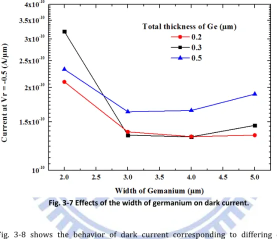
As to alterations in width parameters, the effects of width of germanium body (wGe) and doping separation (Wi) on dark current are discussed in this section. In Fig. 3‐7, it shows effects of width of germanium on dark currents in devices with three different thicknesses, while holding Wi and other parameters fixed. A trend can be seen that dark current is lower as wGe is at around 3 µm to 4 µm for each thickness. Fig. 3‐7 Effects of the width of germanium on dark current.Fig. 3‐8 shows the behavior of dark current corresponding to differing doping separations (Wi). Dark current increases as doping separation gets wider, and the change is much larger than the effect of thickness or width of germanium (wGe).Similar trends show in samples with different thickness. Note that x‐axis of Fig. 3‐8 is the ratio of Wi over wGe, so that effects of wGe is excluded.
Fig. 3‐8Dark current of different diodes versus doping separation ratio.
For a photodiode with fixed wGe, when Wi gets wider, traps in intrinsic region are uncovered by doping regions where carrier concentrations are very high. Although the peak value of electric field decreases as intrinsic region gets wider under same bias (see Fig. 3‐9), dark current still ramps up as long as more and more traps are exposed out and located at a rather high field region. To conclude, the location of traps is critical. When the number of traps that located at large electric field region is increased, not only the generation sites are increased, the generation process becomes more severely as well.
Fig. 3‐9 Electric field distribution in diodes with different doping separation.
3.3.3 Alterations in implant energy
Implant energy determines junction depth. Fig. 3‐10shows dark current of germanium photodiode as a function of implant energy (presented in E/E0 ratio,
where E0 is the original implant energy). Dark current becomes higher when
junctions become shallower. In Fig. 3‐11 it can be seen that as junction depth decreases, electric field spreads out more such that it promotes SRH generation process. Fig. 3‐10 Dark current versus implant energy ratio. Fig. 3‐11 Electric field distribution of diodes with different junction depth .
3.4 Conclusion
In this chapter, TCAD simulation is involved. In the beginning, models used in our simulation are introduced, including SRH model. Then base structures with estimated defect density are built via TCAD sprocess tool; the estimated defect densities are 5e18/cm3 and 1e20/cm3 for simulations of constant defect profile and
exponential defect profile respectively. Finally we make alteration in the base structure and show an optimum structure that has minimum dark current.
Generally speaking, to make a germanium photodiode with low leakage, a thin germanium layer is required to reduce the SRH volume (number of traps) as much as possible, a narrow doping separation is crucial to keep a small SRH volume within this large electric field region, and finally deep junctions are needed to circumvent the spreading electric field.
Chapter 4
Quantum Efficiency
Optimization
In this chapter, an optical signal in implanted into the base structure obtained in chapter 2 as an input to simulate the illuminated photodiode. Optical generation method and definition of quantum efficiency (QE) are given. And again, we make alteration in the base structure and show an optimum structure that has maximum quantum efficiency.
4.1 Optical Generation and definition of Quantum Efficiency
4.1.1 Optical Generation Method
As shown in Fig. 4‐1, a two‐dimensional single‐mode light intensity distribution of infrared optical signal at 1550 µm inside a two‐dimension Germanium structure of 2‐ μm‐wide and 0.2‐μm‐thick was obtained beforehand by using the commercial propagation tool FIMMWAVE by Photon Design (Photon Design, Inc., Oxford, U.K.). FIMMWAVE is a fully vectorial mode finder which provides rigorous solutions to the full Maxwell equations. It can quantitatively simulate the modal behavior and optical properties inside waveguides of arbitrary material and of almost any shape. Fig. 4‐1 The 2Dsingle‐modeinfrared light intensity distribution inside a 2D Germanium structure of 2‐μm‐wide and 0.2‐μm‐thick.
From the result obtained by FIMMWAVE, the intensity distribution is found to be a two‐dimensional Gaussian form with specific variance (
σ
x2,σ
y2). Then, opticalcommand codes expressed by two‐dimensional Gaussian are added in TCAD simulator (codes in appendix) to mimic one photon in GePD. and the number we use in the following optimization simulations is 1e15 (cm‐3s‐1).Fig. 4‐2 shows the
illustration of light intensity in 2D Gaussian form and the GePD cross‐section after optical signal is plugged in.
Fig. 4‐2 Two‐dim Gaussian optical signal in the TCAD simulator.
(Top) Illustration of light intensity in 2D Gaussian form; (bottom) GePD cross‐section after optical signal is plugged in.
4.1.2 Definition of Quantum Efficiency (QE)
Quantum Efficiency(QE), or external quantum efficiency (EQE), is defined by the ratio to the number of incident photons of a given energy over the number of electrons that collected by photodiode, which is shown at Eq. 4‐1.The value of quantum efficiency indicates the ability of a photodiode to transfer optical signal into electrical signal and collect them.
EQE number of electrons/sec
number of photons/sec Eq. 4‐1
Another type of quantum efficiency is internal quantum efficiency (IQE), which is not used in the evaluation of our simulated photodiodes. The value IQE indicates the photon transmission ability of photodiodes, which is not the issue concerned in this thesis.
4.2 QE in respect of Structural parameters
Alterations are done mainly in total thickness of germanium, width of germanium, and the doping separation.4.2.1 QE dependence on thickness and width of GePD
In Fig. 4‐3, light distribution in photodiodes with various geometries is shown. One can see in small GePD, light intensity concentrates in the middle of the photodiode, where electric field is the largest. This is beneficial because the generated carriers can be quickly swept to electrodes by the strong electric field before they recombine. However, there are also lost of lights since some of lights distribute into oxide and silicon. And in the case of wide devices, light distribution broadens out, so averagely the number of carriers generated by photons that experience large force is reduced. Fig. 4‐3 Light distribution in photodiodes with different width and thickness. As a result, we can expect an optimum happen at a specific germanium thickness and width. As shown in Fig. 4‐4, maximum value happens at thickness of 0.5 µm and total Ge width of 3.4 to 4.5µm.
Fig. 4‐4 Effects of Ge thickness and width on QE.
4.2.2 QE dependence on doping separation
In this section, photodiodes including different doping separation (Wi) are simulated with the GePD obtained in previous section that have lights mostly concentrate in the middle, and also be enclosed inside germanium layer. The width of doping separation determines firstly the window that enables electric field to act on generated electrons and holes, and secondly the strength of the electric field.
A large Wi indicates a large window to capture light, nevertheless we have shown in Fig. 3‐9(show again below)that electric field decreases as Wi increases. That is, we should make Wi large enough to capture sufficient light, but not so large that electric field becomes too weak to drive electrons and holes to electrodes before they recombine. Fig. 3‐9 Electric field distribution in diodes with different doping separation. Fig. 4‐5 shows how QE depends on doping separation. It can be seen that quantum efficiency reaches a maximum when Wi is 50% to 60% of the total width of germanium.
Fig. 4‐5 QE dependence on doping separation.
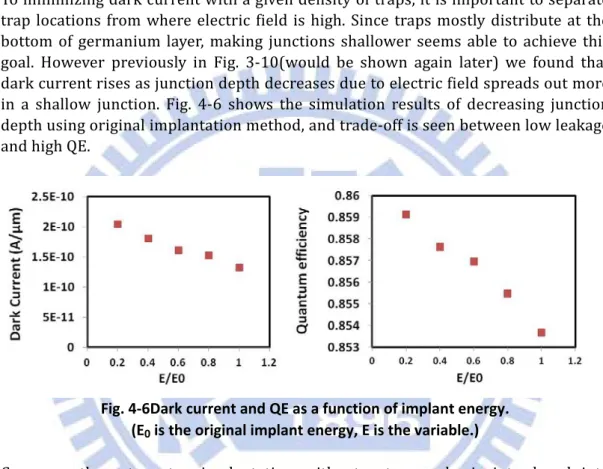
4.3 QE improvement by Junction engineering
From the results of chapter 3 and previous sections in this chapter, one sees there is inevitable trade‐off between low dark current and high QE. In this chapter, junctions engineering is performed and attempted to maintain or increase quantum efficiency at the same time keeping dark current at a low level. To minimizing dark current with a given density of traps, it is important to separate trap locations from where electric field is high. Since traps mostly distribute at the bottom of germanium layer, making junctions shallower seems able to achieve this goal. However previously in Fig. 3‐10(would be shown again later) we found that dark current rises as junction depth decreases due to electric field spreads out more in a shallow junction. Fig. 4‐6 shows the simulation results of decreasing junction depth using original implantation method, and trade‐off is seen between low leakage and high QE. Fig. 4‐6Dark current and QE as a function of implant energy. (E0 is the original implant energy, E is the variable.)Consequently, a two‐step implantation without extra masks is introduced into simulator, as the first implantation to form a deep junction with small doping concentration, and the second one to form a shallow junction with high doping concentration. The function of deep junction is to screen out the spreading electric field from the shallow junction, while it itself provides very small electric field so that SRH process through traps at the bottom of GePD wouldn’t be very strong. Illustration of deep‐and‐shallow doping and the simulated structure with E/E0 =0.2
are in Fig. 4‐7.
Fig. 4‐7 Deep junctions and shallow junctions.
Results of simulation of deep‐and‐shallow junctions are in the following. Fig. 4‐8 shows dark current and QE as a function of shallow doping dosages, and a set of curves differing by deep doping dosage is presented. Shallow doping concentration can be as heavy as activation maximum (for germanium is approximately 1e19/cm3),
since high QE is achieved without promoting dark current. Dark current is suppressed compared to that of structure without the second step deep doping, and implantation dose of 3e13/cm2is chosen to be the optimum doping concentration for deep junction. Doses as low as 5e12/cm2 for deep doping cannot sufficiently screen out the electric fields form shallow junctions, and deep junctions with doses larger than3e13/cm2might provide its own electric field and resulted in dark current rising, such as the behavior of devices with 5e13/cm2(red line with square). Fig. 4‐8 Effects of deep‐and‐shallow junctions on dark current and QE.
4.4 Conclusion
Here in chapter 4, we start to simulate the photocurrent of GePD with optical signals. Optical signal is generated by putting the Gaussian form calculated by waveguide modal solver.
To have high quantum efficiency, we have an optimum with the width of germanium equals to 3.4 µm, the thickness of germanium equals to 0.5 µm, and the doping separation equals to half of the width, that is 1.7 µm.
To maintain high quantum efficiency while keeping low level of dark current, deep‐ and‐shallow junction is proposed. Deep junction is doped slightly 3e13/cm2 to
suppress dark current, and shallow junction is degenerately doped to prompt photo currents.
The optimum structure is shown in Fig. 4‐9, where the color legend is for dopants and defect concentration, and round contours is illustrating the optical signal inside GePD. Fig. 4‐9 The optimum structure for low dark current and high QE.
Chapter 5
Transient Response
Optimization
In this chapter, the transient respond of photodiode to an optical pulse signal is presented, and the parasitic capacitance of our simulated photodiode without optical signal is obtained by C‐V simulation. In the following sections, an equivalent circuit of GePD is given, the issue of the length of the photodiode is discussed, and finally frequency response of simulated photodiode is shown respectively.
5.1 The Role of Transient Response
The significant growth in computer processing power due to microelectronics scaling requires a corresponding increase in communication bandwidth. For on‐chip applications, detectors with very small capacitance and high speed are crucial for low power, large bandwidth systems[17].
To estimate the transient behavior intrinsically from GePD device, an optical pulse signal is introduced into the TCAD simulator, while the simulated photodiodes are in the operation point ‐0.5V. Next we characterize the speed of simulated germanium photodetector in a unit of GHz by calculating the inverse of Rise Time, which is defined by: The time required for the response to rise from 10% to 90% of its final value. As shown in Fig. 5‐1. Fig. 5‐1 Illustration of rise time definition.
To estimate the input‐output transient respond from the system point of view, Fig. 5‐2 shows the equivalent circuit of a P‐i‐N photodiode.
A photodiode is regarded as a current source with parasitic leakage resistance and junction capacitance, and parasitic capacitance, resistance and inductance of interconnect would also contribute to RC time delay. As Iph is changing with the AC
optical signal, the voltage–drop across is Rs also changing, and this leads to the
charging/discharging behavior of CPD and CP.The ultimate goal is to acquire an
equivalent circuit model of GePD, and after seeing the intrinsic speed of GePDs with different geometry in section 5.2, the value of component CPD is obtained from C‐V
simulation in section 5.3. Fig. 5‐2 Effective circuit of a PIN photodiode[20][21].
5.2Speed in respect of structural parameters
In this section, the effects of doping separation (Wi) and width of germanium (wGe) on the photodiode capacitance and speed are discussed. C‐V characteristic simulation is first performed on photodiodes with different Wi and wGe without injecting optical signal. Subsequently, an optical input with pulse width equals to 1 nanosecond is introduced into the electrical characterization section in simulator, and then speed (GHz) is calculated via rise time of the responds corresponding to every device.
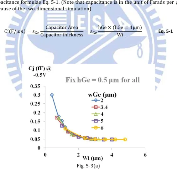
Fig. 5‐3 shows the C‐V characteristics of simulated photodiode with various structures, and one sees from Fig. 5‐3 (a) that capacitance increases dramatically as Wi decreases, and from Fig. 5‐3 (b) capacitance increases as hGe increases, while wGe plays little role in capacitance. It is quite reasonable when seeing a well‐known capacitance formulae Eq. 5‐1. (Note that capacitance is in the unit of Farads per µm, because of the two‐dimensional simulation) C F/μ ε Capacitor Area Capacitor thickness ε hGe LGe 1μm Wi Eq. 5‐1 Fig. 5‐3(a)
Fig. 5‐3(b)
Fig. 5‐3 C‐V characteristics of simulated photodiode with various structures.
However, in Fig. 5‐4speed dependencies on wGe appear to have an inverse linear relation despite the fact that wGe has little contribution to parasitic capacitance. (Note that Wi is fixed). It can be explained by the transition time for carriers to travel to electrodes, since there is a longer distance for electrons that generated in the middle of GePD to be driven to cathode in a rather wide photodiode, vice versa for holes. Fig. 5‐4 Speed of GePD is inversely proportional to wGe.
In Fig. 5‐5, speed above 30GHz is achieved in the device wGe equals to 2 µm, with doping separation equals to 1.2 µm. The photodiode with the structure which provides best quantum efficiency is indicated as well. Speed distribution over doping
separation is pretty sharp, and two machismos competing with each other. At region I, speed is affected by the large junction capacitance when Wi is small, In region II, speed is limited by the transition velocity of carriers since electric field decreases Wi increases. Fig. 5‐5.Speed evaluation of GePDs with different Wi and wGe.
5.3 Length effect
In previous chapters, simulations are all done in a two‐dimensional germanium photodiode; therefore in this section, we consider the effects of the length (LGe) on photodiode (L is shown inFig. 2‐4), including the capacitance and the absorption efficiency of lights in long and short devices.
5.3.1 Capacitance in length direction
First estimation of transient respond of germanium photodiode is required from a system level point of view. To reduce RC delay, the capacitance of germanium photodetector for interconnect system should always be minimized. Fig. 5‐6 shows the parasitic capacitance CPD at ‐0.5V. In the structure of GePD in this thesis, the
length of electrodes is approximately same with the length of implant junctions. Since capacitance is increasing with the GePD length, a short germanium photodiode is desirable for both lowering CPD and pad capacitance CP. Fig. 5‐6Parasitic Capacitance CPDobtained with length of GePD.
5.3.2 Absorption in length direction
From the transmission point of view, absorption coefficient measures how quickly the light signal would lose intensity due to the absorption of a material. But, as for photodiode, the more lights absorbed means the more photons can be utilize and contribute to carriers. In Fig. 5‐7, the optical absorption of crystalline Si1‐xGex and the corresponding index of refraction of each material are shown from the literature[22]. Fig. 5‐7 Optical absorption coefficient of Si, Ge, and SiGe alloys[22].
Based on Beer‐Lambert law (Eq. 5‐2), where I, I0, and α are intensity at L, input
intensity and absorption coefficient respectively, the absorption ration as a function of the length of germanium photodiode can be calculated, as shown in Fig. 5‐8. High absorption ration means that there are more number of photons that can be transferred into carriers, so photo‐current would increase. (Note that QE doesn’t change.)
I I ∙ e Eq. 5‐2
Fig. 5‐8 Absorption ratio versus length of germanium photodiode.
As a result, this section reminds that in realist case, although we prefer a short photodiode to avoid large capacitance, the length of germanium photodiode still needs to be compromised with the absorption efficiency of light signals.
5.4 Frequency response
5.4.1 Bit stream input
As an input, the bit stream below in Fig. 5‐9is pseudo random and has the most important transitions because it includes all the combinations of three bits. Fig. 5‐9 The bit stream input contains combinations three bits.
5.4.2 Eye diagram
To evaluate system speed, eye diagrams are often used. An open eye interprets the nice transient respond of an electronic device. In Fig. 5‐10, simulations of transients responds to the bit stream inputs with frequencies 1GHz, 10GHz, 20GHz, 40GHz, and 100GHz are performed. A regular trend can be seen that as the signal frequency is higher than the speed that GePD can handle with, signals distortion can be read as the “eye” getting closed. In realistic cases, eye diagrams needs to be extended with parasitic components, noises, and loads of amplifiers, depending on various interconnect systems.
Fig. 5‐10 Eye diagram of the GePD with speed 30GHz.
5.5 Conclusion
In this chapter, it is seen that the speed of GePD increases with the total width (wGe), while for each wGe there is an optimum doping separation (Wi) value. A maximum 32GHz is found at wGe equals to 2 µm, and Wi equals to 0.2 µm. For optimization in length direction, we should note that length of GePD needs to be compromised with the absorption efficiency of light signals and the junction capacitance.Value of junction capacitance of GePD with different length is obtained by C‐V simulation. The simulation of C‐V might seem redundant, since capacitance is of course increasing linearly with effective capacitor area (hGe × LGe), but it helps us to demonstrate the model of equivalent circuit of GePD, which would be shown in chapter 6.
Finally, frequency respond is shown in eye diagrams while a bit stream of optical signal with various frequencies.
Chapter 6
Conclusion
As one of the crucial components in optical interconnect system, germanium photodiodes are promising due to its corresponding bandgap to absorb infra‐red light and the compatibility to silicon‐based photonics and electronics. However, many researchers have shown that GePD is suffering from high dark current, and efforts were done to suppress the dark current and to increase gain‐bandwidth product by improving GePD efficiency and speed.
Several guidelines toward the GePD structure are provided in this thesis with the aid of investigation of measured dark current and TCAD simulation, to help fabricating high‐efficiency and low‐power consumption germanium photodetector with the structure resembles following figure. A table of guidelines is put at the end of this chapter after statements of conclusions chapter by chapter.
In chapter 2, we show the investigation of physical mechanisms behind the dark current in germanium photodiode via experimental data. It can be verified that dark current is in the combination behavior of diffusion current and Shockley‐Read‐Hall generation current. At room temperature, and at the bias ‐0.5V, SRH generation is the main component in dark current. There is a good qualitative agreement between formula trend and measured data.
In chapter 3, TCAD simulation is involved with inclusion of SRH model. We constructed base structures similar to measured photodiodes in TCAD sprocess tool with defect densities are estimated as 5e18/cm3 and 1e20/cm3 for simulations of
constant defect profile and exponential defect profile. Alterations were made in the base structures to find the structure that has minimum dark current. Generally speaking, to make a germanium photodiode with low leakage, a thin germanium layer is required to reduce the SRH volume, i.e. number of traps, as much as possible. A narrow doping separation is crucial to keep a small SRH volume within the large electric field region. Finally, deep junctions (junction depth ≈ hGe) are needed to circumvent the dark current arouse by the spreading electric field of shallow junctions.