國
立
交
通
大
學
材料科學與工程學系
博士論文
選擇性沉積碳奈米結構圖案之奈米操控
與場效發射研究
Nano-manipulation and field emission study of the
selectively grown carbon nanostructures pattern
研 究 生:林貞君
指導教授:郭正次 教授
潘扶民 教授
選擇性沉積碳奈米結構圖案之奈米操控與場效發射研究
Nano-manipulation and field emission study of the selectively
grown carbon nanostructures pattern
研 究 生:林貞君 Student: Chen-Chun Lin 指導教授:郭正次 教授 Advisors: Prof. Chen-Tzu Kuo
潘扶民 教授 Prof. Fu-Ming Pan
國立交通大學 材料科學與工程學系
博士論文
A Thesis
Submitted to Department of Materials Science and Engineering College of Engineering
National Chiao Tung University in partial Fulfillment of the Requirements
for the Degree of Doctor of Philosophy
in
Materials Science and Engineering
January 2009
Hsinchu, Taiwan, Republic of China
選擇性沉積碳奈米結構圖案之奈米操控與場效發射研究
研究生:林貞君 指導教授:郭正次 教授 潘扶民 教授 國立交通大學 材料科學與工程學系摘 要
操控碳奈米結構(CNSs)沉積的位置、密度與排列方向為目前碳奈米技術主要的研究 課題之一,本研究主要目的為開發在指定的區域沉積具有方向性排列的CNSs 製程,並 且量測其結構與性質特性,使用的三種製程包含陽極氧化鋁(AAO)模板及觸媒輔助方 法、無電鍍觸媒輔助法及電泳輔助沉積法。在CNSs 的結構與性質分析方面,包含 SEM、 EDS、TEM、HRTEM、Raman、AES,及場效發射電性量測;利用紫外可見光吸收光譜 (UV-Vis absorption spectroscopy)及界達電位量測(Zeta potential measurements)進行 CNSs 懸浮液之穩定性分析。 第一種製程是AAO 模板及觸媒輔助方法,首先在矽基材上沉積鋁膜,利用兩階段 陽極氧化處理製備出具有均勻孔洞大小直徑約80 nm、厚度約 550 nm 的奈米孔洞作為 模板,以電鍍法沉積鈷觸媒於 AAO 孔洞內,再以電子迴旋共振化學氣相沉積法合成 CNSs,為製作場發射陣列,SiO2介電層與Al 閘極層分別沉積於 CNSs 上,經黃光製程 後利用乾式與濕式蝕刻方法顯露出場發射區域。在模板輔助成長下,當電鍍鈷觸媒的時 間為45 s 時(高度約 48 nm),CNSs 的平均直徑約 22 nm,密度約 37 #/μm2;當鈷電鍍時 間增加為90 s 時(高度約 84 nm),CNSs 的直徑約 53 nm,密度約 162 #/μm2。為了解CNSs 在受限制的AAO 通道內如何成長,提出一個可能的成長機制。CNSs 大部份為頂端成長 模式,並且存在一個最佳的鈷觸媒電鍍時間60 s,CNSs 的平均直徑約 25 nm,密度約 45 #/μm2,具有較佳的場發射特性(起始電場為 5.1 V/μm),其相對應製作的 CNSs 場發 射陣列具有起始電壓8.1 V/μm 的場發射特性。此方法可以彰顯以 AAO 做為模板,可以 有效的控制CNSs 場發射陣列的結構與特性 第二種製程是無電鍍觸媒輔助法,其主要的目的為利用微波電漿化學氣相沉積系統 在具溝槽之圖案矽基材上,選擇性成長水平奈米碳管(CNTs)橫跨其溝槽。此製程之選擇 性是利用無電鍍法在觸媒於無晶矽層(a:Si)上析出觸媒金屬之化學反應性甚大於氮化矽 層(Si3N4),而 Si3N4層設計鍍在 a:Si 層上,可導引 CNTs 水平成長方向成長。結果顯示 CNTs 主要為竹節狀多壁結構,管壁石墨層數約 20~30。CNTs 的電導性可經由 760oC 的熱退火後,得到很大的改善。結果展現水平成長 CNT 之數目可藉由觸媒電鍍時間與 溝槽寬度來調控。本製程亦具有製造奈米元件導線之潛力。第三種製程是 CNSs 電泳輔助沉積法,利用電泳沉積法(EPD)及後續的退火處理將 單壁奈米碳管(SWNTs)選擇性沉積在各種材料或圖案上。此 EPD 製程首先將 SWNTs 與 三種分散劑或界面活性劑(SDS、TOPO、CTAB)配製成 CNTs 懸浮液。結果顯示就 SWNTs 的分散性及懸浮液穩定性而言,SDS 為最好的界面活性劑。EPD 製程參數中,除了 CNT 的濃度之外,對於薄膜場發射與附著性並無顯著的影響。然而要改善薄膜與基材間的附 著性需要施予較高的退火溫度加上適當的退火時間,並因而降低電阻,提高場發射特 性。高效率的退火薄膜具有小的內應力,其結構往往是由許多微米大小的島狀結構組 成,而小島間有許多水平排列的CNTs。另外,就應用 EPD 製程於不同基材的可行性, 例如導電玻璃,其圖案是由具有導電及不導電材料所組成(Al 和 SiO2),或在不同形狀 基材之可行性,例如彎曲的鋁箔紙,本製程可以成功的用來選擇性沉積CNTs 圖案。
Nano-manipulation and field emission study of
the selectively grown carbon nanostructures pattern
Student: Chen-Chun Lin Advisors: Prof. Cheng-Tzu Kuo Prof. Fu-Ming Pan
Department of Materials Science and Engineering National Chiao Tung University
Abstract
How to deposit or manipulate the carbon nanostructures (CNSs) with the desired orientation, number density and locations to form patterns is one of the key issues for fabricating the nanodevices. The purpose of this research is to develop nanofabrication processes to manipulate the CNSs patterns and to examine their structures and properties. The developed processes may be roughly divided into three categories, including the anodic aluminum oxides (AAO) template-catalyst-assisted, the electroless plating catalyst-assisted, and CNSs-electrophoresis-assisted processes. The structures and properties of the CNSs and their patterns were characterized by SEM. EDS, TEM, HRTEM, Raman, AES, and field emission I-V measurements. The stability of CNSs-suspensions was evaluated by UV-Visible absorption spectroscopy and Zeta potential measurements.
For the AAO template-catalyst-assisted process, nanoporous AAO template was first prepared by a two-step anodization process on the Si(100) substrate with 80 nm in diameter and 550 nm in depth, followed by Co catalyst and the vertically aligned CNSs deposition in AAO pore channels by electron cyclotron resonance chemical vapor deposition (ECR-CVD). The field emitter arrays were further prepared by directly depositing SiO2 dielectric and Al
gate layer on the CNSs. Reactive ion and wet etches were then used to open the field-emission area. The results show that the average diameters and the corresponding number density of the AAO-assisted CNSs vary from 22 nm, 37 #/μm2 to 53 nm, 162 #/μm2 for Co deposition times
of 45 s (~ 48 nm in height) and 90 s (~ 84 nm in height), respectively. A mechanism is first proposed to delineate the CNS growth in a confined pore channel space of the AAO template. The CNSs are mainly the tip-growth type in structure and there is existence of an optimum field emission turn-on field of 5.1 V/μm for AAO-assisted CNSs with ~ 25 nm in diameter and ~ 45 #/μm2, which is corresponding to the turn-on field of 8.1 V/μm for the emitter array.
The results had demonstrated that the structure and properties of CNSs emitter array can be effectively manipulated by this AAO template-assisted process.
For the electroless plating catalyst-assisted process, the main purpose was to selectively grow the horizontally-oriented carbon nanotubes (CNTs) across the trenches of the patterned Si wafer in a microwave plasma CVD system. The CNT selectivity of the process is based on
the greater chemical reactivity of the catalyst with a:Si than with Si3N4, where the Si3N4
barrier layer of the pattern was designed on top of the a:Si layer to guide the growth of CNTs in horizontal direction to bridge across the trenches of the pattern. The CNTs are mainly bamboo-like multiwalled CNTs (MWNTs) with a wall thickness of 20~30 graphene layers. Its electrical conductivity can be greatly improved by subjecting to 760oC heat treatment under nitrogen atmosphere. The results demonstrate that the amounts of the horizontally-oriented CNTs are tunable with the Ni catalyst plating time and the trench width. This process also demonstrates the potential for nano-connecter fabrication in nano devices.
For CNSs-electrophoresis-assisted method, electrophoretic deposition (EPD) followed by post air annealing treatment was developed to selectively deposit the single-walled CNTs (SWNTs) on various substrates or patterns. The EPD was conducted from a solution mixture of SWNTs and various dispersants or surfactants, including sodium dodecyl sulfate (SDS), hexadecyl trimethyl ammonium bromide (CTAB) and trictylphosphine oxide (TOPO). The results indicate that the SDS is the best surfactant in terms of SWNTs dispersion and solution stability, and the EPD parameters, except CNTs concentration in the suspension, have no significant effects on their field emission (FE) and adhesion properties of the deposited films. However, a higher post annealing temperature combined with an optimum annealing time is required to improve the film-substrate adhesion, so to reduce its electrical resistance and to enhance FE properties. The high performance annealed films with negligible internal stress are made of the micro-sized islands with the horizontally oriented SWNTs between them. On feasibility to apply the EPD process on other substrate materials such as ITO, the pattern made of conductive and nonconductive coatings (Al and SiO2), or the substrates with different
shapes like curved Al-foil, can be successfully used to selectively deposit CNTs pattern by EPD.
Acknowledgements (謝辭)
首先,學生由衷地感謝 郭正次教授與 潘扶民教授的耐心指導、論文寫作技巧方面的悉心教誨、提 供齊全的研究設備與資源,並且在待人處世方面給予提醒與啟發,使我受益匪淺,謹此致以最誠摯的謝 意。同時感謝考試委員成大機械系 李驊登教授、交大材料系 張立教授、逢甲材料系 何主亮教授、中興 材料系 呂福興教授、北科大機械系 林啟瑞教授的親臨指導,有了您的寶貴意見與指導,使得本論文更 具完整性。 家人的支持是我最重要的力量,首先感謝我的最佳智囊團帥爸爸還有俏皮可愛的媽媽,每當我在學 校遇到煩惱的事情或是身體不舒服的時候,最愛回到溫暖的家了,也希望爸爸媽媽的身體健康,我終於 要出去賺錢了,你們可以多安排一點休閒活動,好好享受一下;跟我一起住的體貼型男弟弟保鏢,每當大 風大雨或是太晚回家的時候就變成我的司機,真的我幫了不少忙,希望你的學業還有以後的工作都能順 順利利;生活多采多姿又越來越漂亮的妹妹,少了愛打扮的妳時時叮嚀我,我都變醜了啦!也祝你學業順 利還有天天快樂阿!給我最想念的外公,常常懷念博一住在外公家的日子,祖孫倆一起分享偷偷吃挫冰 的滿足感,每次出國參加研討會您一定舉雙手贊成,還會給我紅包當旅費哩;最時髦最有品味的外婆,您 總是關心我的身體還有近況,絕頂的廚藝、風趣的談吐總是讓大家充滿歡樂,希望您的身體健康,永遠 美麗。還有感謝最多鬼點子的阿姨還有最愛玩的小舅,每次的家庭聚會總是獨一無二歡樂無窮,是最好 的放鬆劑了。 感謝好朋友們的鼓勵與陪伴,首先是最捨不得的好朋友澎澎,本來說好要來參加我的畢業典禮的, 我們總是分享生活中大大小小的事情,一起經歷快樂還有傷心,你也總是給我最大的鼓勵,要我克服困 難,謝謝妳,我永遠都會想念妳的;最喜歡給我驚喜的小倩,雖然平常大家各忙各的,但是你就是三不五 時會來看看我這個老朋友,讓我知道你一直有在關心我,我每次都很感動的,也祝你早日畢業,我也會 三不五時幫你加油的喔!給有著堅強毅力的 Shally,你是我的力量加油站,也是最會叮嚀我的造型顧問, 希望你趕快學成歸國阿;還有一同從碩士開始奮鬥的心心與庭庭,有你們的相挺,研究的路上不孤單,也 希望你們都能一切順利,還有趕快找到另一半囉;還有重要的 Kaoming,總是在我身邊照顧我、給我力量, 是我的一大精神支柱阿,希望你能天天開心、心想事成啦! 感謝一起作實驗打拼的伙伴,凱鈞、盈君還有全雯,有了你們大力的幫忙,我的論文才能完整。同 窗副修體育系的室長必愷,肩負著設備工程師的使命,也帶領著固定運動的氣氛,我們可是每年都有得 到環校路跑的運動衫呢!希望你身體健康,還有早日畢業喔!最仔細、貼心的伊茹,不管在學業或是生 活中,總是感受到你的體貼,我們的葡西之旅還有每年的生日心機都是令人難忘的一段回憶,祝福你趕 快實現夢想!旅遊伙伴的第一人選還有購物達人淑筠,每次跟你出去玩怎麼覺得就是特別的瘋狂好玩, 要買東西或是學校裡面大大小小的事情問你就對了,真是太高興有你這麼好的助理與朋友!才剛開始熟的 泰瑞,你的熱情開朗還有真誠是我覺得最難得的,希望你能繼續保持下去,並且一切順利啦。另外,感 謝柏林學長、兆焄學長、威翔學長、德銘學長在實驗上的建議,謝謝協宗、岳翰、玉容、祐君、土狼、 峻愷、國銘、奕同、詩容、淑幸、蝗蟲、文綬、立群、碩傑、宜學、怡萱等等在實驗與生活上的協助。 同時要感謝華映與莫處長提供產學合作的機會與獎學金,並謝謝劉梅、美昭的照顧。 最後,再一次跟大家說聲謝謝,很高興在交大這段期間,可以認識大家,讓我的生活更豐富。Contents
Abstrate in Chinese (摘要)...I Abstract in English ...III Acknowledgements in Chinese (謝辭)... V Contents ...VI List of Symbols... VIII Table Caption... X Figure Caption ...XI
Chapter 1 Introduction...1
Chapter 2 Literature Review ...3
2.1 Overview of the CNSs...3
2.2 Applications of the CNSs ...7
2.3 Selective deposition methods for the nanostructures ...17
2.4 Fabrication methods for the oriented CNSs ...23
2.5 Analysis methods of the CNSs ...26
2.5.1 Morphologies, and lattice image analyses...26
2.5.2 Bonding and crystal structure analyses ...27
2.5.3 Electrical, optical and thermal properties measurements ...28
Chapter 3 Experimental Methods...30
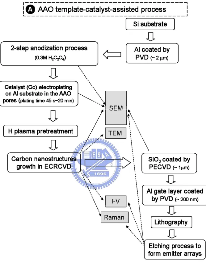
3.1 Experimental flowcharts...30
3.2 AAO template-catalyst-assisted process...34
3.2.1 AAO-template preparation by anodization process...34
3.2.2 Catalyst deposition in the nanopores of AAO template by electroplating ...36
3.2.3 CNSs deposition by ECR-CVD...36
3.2.4 Fabrications of the emitter arrays on the AAO-assisted CNSs...37
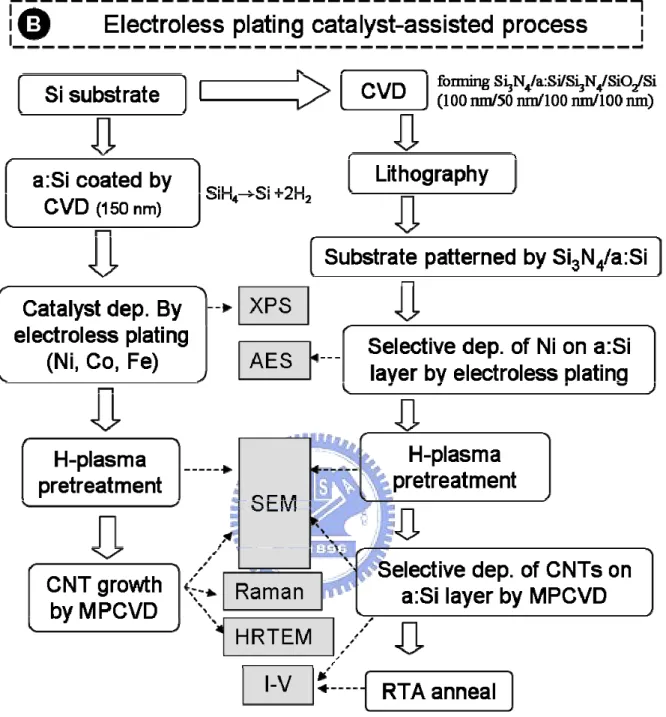
3.3 Electroless plating catalyst-assisted process ...40
3.3.1 Substrate preparation for selective deposition of catalyst ...40
3.3.2 Catalyst deposition by electroless plating ...41
3.3.3 CNTs deposition by MPCVD ...42
3.3.4 RTA heat treatment ...43
3.4 CNSs-electrophoresis-assisted process...45
3.4.1 Substrate preparation for selective deposition...45
3.4.2 Suspensions preparation for CNTs dispersion...46
3.4.3 The electrophoretic processes with CNT suspensions...46
3.4.4 Post-annealing ...46
3.5 Structures and properties characterization...48
3.5.2 AES...48
3.5.3 Raman spectroscopy...48
3.5.4 XPS...49
3.5.5 Electrical properties measurement...49
3.5.6 UV-Vis spectroscopy and Zeta potential measurement ...50
Chapter 4 Results and discussion for the AAO template-catalyst-assisted CNSs emitter arrays ...52
4.1 Morphologies of AAO template and Co catalysts in nanopores ...52
4.2 Effects of the Co plating time on the AAO template-catalyst- assisted CNSs ...54
4.2.1 On morphologies of the CNSs...54
4.2.2 On Raman spectra and TEM images of the CNSs...55
4.2.3 On number density of the CNSs and growth mechanism discussion...59
4.2.4 On field emission properties of the CNSs ...63
4.3 Effects of the processing parameters of the field emitter arrays ...64
4.3.1 Effect of the CNSs growth time on SiO2 film morphology...64
4.3.2 Effect of the etching times and methods on emitter morphology and CNSs Raman spectra ...65
4.4 Field emission properties of the emitter arrays ...69
4.5 Summary...70
Chapter 5 Results and discussion for the electroless plating catalyst-assisted process...71
5.1 Compositions of the catalyst films by XPS and EDS...71
5.2 Morphologies and lattice images of the catalyst nanoparticles and the as-deposited CNTs...74
5.3 Auger spectra at different positions on the Ni catalyst-deposited pattern ...78
5.4 Morphologies at trench on the pattern with the Ni-assisted CNTs...79
5.5 I–V curves of the pattern with the horizontally-aligned CNTs across trenches ...82
5.6 Summary...83
Chapter 6 Results and discussion for the CNSs-eletrophoresis-assisted process...84
6.1 Raman spectrum of the raw SWNTs ...84
6.2 Effect of the surfactant type on stability of SWNT suspensions ...85
6.3 Effect of post annealing on morphologies and field emission properties of the CNSs-EPD-assisted films...88
6.4 CNSs deposition selectivity of the pattern components by EPD ...91
6.5 Substrate diversifications of the EPD process...92
6.6 Summary...93
Chapter 7 Conclusions...94
Chapter 8 Future Prospects...96
List of Symbols
A Absorbance AAO Anodic aluminum oxide
a:C Amorphous carbon
AES Auger electron spectroscopy AFM Atomic force microscope
a:Si Amorphous silicon
BE Binding energy
BOE Buffered oxide etchant
CNFs Carbon nanofibers
CNSs Carbon nanostructures
CNT-FETs Carbon nanotube -field effect transistors
CNTs Carbon nanotubes
CTAB Hexadecyl trimethyl ammonium bromide CVD Chemical vapor deposition
DSSC Dye-sensitized solar cells
ECR-CVD Electron cyclotron resonance chemical vapor deposition EDS Energy dispersive spectroscopy
EF Energy level of the free electrons
Eto Turn-on field
EPD Electrophoretic deposition φ Work function
FE Field emission
FIB Focused ion beam F-N Fowler-Nordheim
HDP-RIE High density plasma reactive ion etching
HRTEM High resolution transmission electron microscopy
I The intensity of light passing through a sample
Io The intensity of light before it passes through the sample
I / Io or %T Transmittance or express in percentage (%T)
LPCVD Low-pressure CVD
Mion Metallic ions
MPCVD Microwave plasma chemical vapor deposition MWNTs Multi-walled carbon nanotubes
OPVs Organic photovoltaic devices PL Photoluminescence
RIE Reactive ion etching
RTA Rapid thermal annealing RBM Radial breathing mode
STM Scanning tunneling microscopy SDS Sodium dodecyl sulfate
SEM Scanning electron microscopy SWNTs Single-walled carbon nanotubes TEM Transmission electron microscopy
TGA Thermogravimetric analysis
TOPO Trioctylphosphine oxide UV-Vis Ultraviolet-visible
Table Caption
Table 3-1 Specimen designations of the AAO-assisted CNSs and their deposition conditions ...39 Table 3-2 The compositions of the electroless solutions...41 Table 3-3 Specimen designations of the electroless plating catalyst-assisted CNTs and their
deposition conditions...44 Table 3-4 Suspension designations and their compositions. ...46 Table 3-5 Specimen designations of the CNSs-EPD-assisted films and their deposition
parameters...47 Table 5-1 Comparison of the features of the electroless plating catalyst-assisted carbon
Figure Caption
Fig. 2-1 Eight allotropes of carbon: (a) Diamond, (b) Graphite, (c) Lonsdaleite, (d) C60, (e)
C540, (f) C70, (g) Amorphous carbon, and (h) Single-walled carbon nanotube
[http://en.wikipedia]. ...3
Fig. 2-2 Ternary ‘phase’ diagram of carbon allotropes. P/H corresponds to the ratio of
pentagonal/hexagonal rings [Heinmann 1997-1654]...5 Fig. 2-3 The three structural forms of carbon nanofibers, classified by the angle of the
graphene layers/platelets with respect to the filament axis [Rodriguez 1995-3862]. ...6 Fig. 2-4 Structures of a graphene sheet, single-walled carbon nanotube and multi-walled
carbon nanotube [http://www.personal.psu]. ...7 Fig. 2-5 Potential-energy diagram illustrating the effect of an external electric field on the
energy barrier for electrons at a metal surface [Cheng 2003-1021]...8 Fig. 2-6 A prototype 4.5 field emission display fabricated by Samsung using carbon
nanotubes [Choi 1999-399]. ... 11 Fig. 2-7 Demonstration of field emission light source using carbon nanotubes as the
cathodes [Saito 1998-L346]. ... 11 Fig. 2-8 Nanoelectronic devices. (a) Schematic diagram for a CNT-FET. The
semiconducting nanotube, which is on top of an insulating aluminum oxide layer, is connected at both ends to gold electrodes. (b) Scanning tunneling microscope (STM) picture of a SWNT field-effect transistor made using the design of (a)
[Bachtold 2001-1317]...12
Fig. 2-9 Use of a MWNT as an AFM tip At the center of the VGCF is a MWNT which forms the tip. The VGCF provides a convenient and robust technique for mounting the MWNT probe for use in a scanning probe instrument [Ajayan 2001-391]. ...14 Fig. 2-10 SEM micrographs showing growth of carbon nanotube obelisks on an array of
submicron nickel dots [Ren 1999-1086]...17 Fig. 2-11 A SEM image of a patterned SiO2/Si substrate exposed to the precursor. Carbon
nanotubes have grown selectively on the SiO2 patterns, with no observable growth
on the Si areas [Zhang 2000-3764]. ...18 Fig. 2-12 (a) Three stages of AAO pore formation (b) The reactions involved in Al
anodization process (c) The size of the pores or their interpore distance versus the applied voltage [Thamide 2002-240; Li 1998-2470; Li 1998-6023]...20 Fig. 2-13 Approaches to carbon nanotube organization: (a) Aligned growth under external
forces, (b) Template approaches, (c) Crowding effect,(d) Postgrowth aligned deposition from liquid dispersions, and (e) Epitaxial approaches [Joselevich 2002-1137; Li,
Fig. 3-1 Experimental flowchart for the AAO template-catalyst-assisted process...31
Fig. 3-2 Experimental flowchart for the electroless plating catalyst-assisted process. ...32
Fig. 3-3 Experimental flowchart for the CNSs-electrophoresis-assisted process. ...33
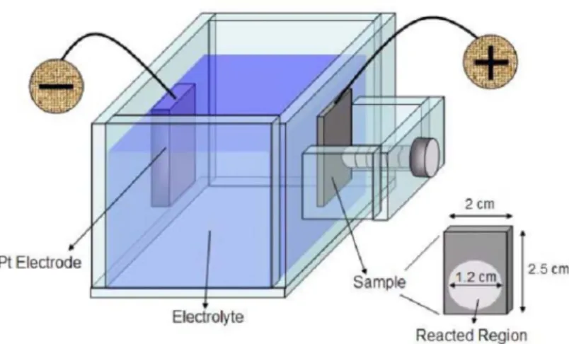
Fig. 3-4 Schematic diagram of the two-step anodization process. ...35
Fig. 3-5 Schematic diagram of experimental setup for the Al anodization. ...35
Fig. 3-6 Schematic diagram of the ECR-CVD system...37
Fig. 3-7 The fabrication scheme of the emitter arrays on the AAO-assisted CNSs: (a) preparation of the AAO layer on the Si wafer, (b) CNS growth by ECR-CVD deposition, (c) SiO2 dielectric and Al gate electrode depositions on the CNSs, and (d) RIE and BOE etches to open the field-emission area...38
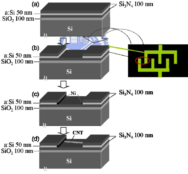
Fig. 3-8 Schematic diagrams showing the electroless plating catalyst-assisted CNTs grown across trenches of a pattern...40
Fig. 3-9 Schematic diagram of the MPCVD system. ...43
Fig. 3-10 Square-shaped pattern made of Al and SiO2 components for EPD process. ...45
Fig. 3-11 Schematic diagram of the field emission measurement setup. ...50
Fig. 4-1 SEM image of the AAO template after two-step anodization process. ...52
Fig. 4-2 Cross-section view of SEM images of the Co-deposited AAO template under different Co electroplating duration: (a) 45, (b) 60, (c) 75, (d) 90, (e) 600 and (f) 1200 s. (For SP. #A2, A3, A4, A5, A7 and A8, respectively.) ...53
Fig. 4-3 The curves showing features of morphologies as a function of the Co plating time in AAO template catalsyt-assisted process: (a) the deposited Co height in AAO, (b) tube diameter of CNSs, and (c) number density of the CNSs. ...54
Fig. 4-4 Top-view SEM images of the as-deposited CNSs under different Co electroplating times: (a) 45, (b) 60, (c) 75 and (d) 90 s. (For SP. # A2, A3, A4 and A5, respectively) ...55
Fig. 4-5. Raman spectra of the as-deposited carbon nanostructures under different Co electroplating times. (SP. #A2-5)...56
Fig. 4-6 Cross-sectional SEM images of the as-deposited CNSs in nanopores of AAO template under different Co electroplating times: (a) 60, (b) 90 and (c) 0 s. (For SP. # A3, A5 and A1, respectively)...58
Fig. 4-7 TEM images of the Co-assisted CNSs: prepared by different sampling techniques: (a) FIB and (b) ultrasonic agitation. (SP. #A6, and A5, respectively) ...58
Fig. 4-8 HRTEM images of CNFs near the tip under different Co electroplating times: (a) 60 and (b) 90 s. (For SP. # A3 and A5)...59
Fig. 4-9 Schematic illustration of carbon nanostructure growth mechanism in the AAO pore channel with different Co plating time: (a) 90 s and (b) 60 s, respectively...62
Fig. 4-10 (a) J-E curves of the as-deposited AAO-assisted CNSs under different Co electroplating times. (SP. #A2, A3, A4, A5, respectively) and (b) is the F-N plot of the SP. #A3. ...64
Fig. 4-11 SEM side view images of the SiO2-coated CNSs for different CNS growth times
(a) 30, and (b) 35 min, respectively. ...65 Fig. 4-12 SEM images of the SiO2-coated CNSs after RIE etch for (a) 240 s, (b) 300 s, (c)
360 s, (d) 420 s, (e) 480 s and (f) higher magnification of (e). (SP. #A9, A11, A12, A13 and A14 respectively) ...66 Fig. 4-13 SEM images of the as-prepared AAO-assisted emitter arrays: (a) top-view of
emitters, (b) higher magnification of (a), (c) side-view of (b), and (d) higher
magnification of (e), respectively. (SP. #A10)...67 Fig. 4-14. Raman spectra of (a) the as-deposited CNSs and (b) the as-prepared
AAO-assisted emitter arrays. (SP. #A3 and A10)...68 Fig. 4-15 (a) J-E curve of the AAO-catalyst-assisted CNSs emitter arrays and (b) is its
corresponding F-N plot. (SP. #A10) ...69 Fig. 5-1 EDS spectrum of the as-plated Ni catalyst films on a:Si/Si substrate by electroless
plating (SP. #B3)...72 Fig. 5-2 XPS spectra of the as-plated catalyst films on a:Si/Si substrates for different
catalyst materials: (a) Co, (b) Fe and (c) Ni. (SP. # B1, B2 and B3, respectively) 73 Fig. 5-3 SEM micrographs of nanoparticles after H-plasma pretreatment for different
catalyst materials: (a) Co, (b) Fe and (c) Ni. (SP. # B1, B2 and B3, respectively) 74 Fig. 5-4 SEM micrographs of the as-deposited CNTs for different catalyst materials: (a) Co,
(b) Fe and (c) Ni. (SP. # B1, B2 and B3, respectively) ...76 Fig. 5-5 Raman spectra of the as-deposited CNTs for different catalyst materials: (a) Co, (b)
Fe and (c) Ni. (SP. # B1, B2 and B3, respectively). ...76 Fig. 5-6 TEM micrograph showing morphology of the as-deposited bamboo-like CNT with
discrete Ni catalyst particles split from one original particle in the tube. (SP. #B3) ...78 Fig. 5-7 HRTEM lattice image of a compartment of the tube around the Ni catalyst. (SP. #
B3) ...78 Fig. 5-8 (a) Schematic diagram showing the AES analytical positions on the patterned
substrate, (b) the corresponding Auger spectra of Ni catalyst at Position 1 or 2, and (c) Position 3, respectively. (SP. #B7) ...79 Fig. 5-9 SEM micrographs of the as-deposited CNTs on the substrate patterned by
Si3N4/a:Si under different catalyst electroless plating times: (a) 10, (b) 15 (c)20
(d)30 and (e) 60 s. (SP. # B4, B5, B6, B8 and B9, respectively)...81 Fig. 5-10 (a) and (b) are two typical SEM micrographs of the as-deposited CNTs across
trenches of the Ni-coated patterns at two different positions of SP. #B7. ...82 Fig. 5-11 I-V curves of the horizontally-oriented CNTs patterns, (a) the as-deposited, and (b) the post-annealed conditions. (SP. #A7)...82 Fig. 6-1 Raman spectrum of raw SWNTs materials, the inset is the corresponding detail of
Fig. 6-2 Pictures of (a) the as-agitated suspensions, and (b) corresponding suspensions after 2 week precipitation. (Suspension designation: S1: SWNTs and D.I. water, S2: SWNTs, SDS and D.I. water, S3: SWNTs, CTAB and D.I. water, and S4: SWNTs and TOPO and butyl alcohol) ...86 Fig. 6-3 UV-Vis absorption spectra of the as-sonicated suspensions (black line) and the
corresponding suspensions after 2 weeks precipitation (grey line) for different suspensions: (a) S1, (b) S2, (c) S3 and (d) S4, respectively. ...86 Fig. 6-4 (a) HRTEM image of the SWNT sonicated for 3 hours in SDS aqueous suspension
(with schematic inset to show the SDS striations), and (b) the corresponding EDS spectrum. ...87 Fig. 6-5 SEM micrographs of the deposited and 3-min-annealed films under same EPD
deposition conditions but different post annealing temperatures: (a) 100oC, (b) 200oC, (c) 300oC (SP. #C6, C8 and C11, respectively) and (d) is the corresponding image of (c) at higher magnification. ...89 Fig. 6-6 J-E curves of the deposited and annealed films on Al-coated Si substrate under
same annealing time (5 min) but different annealing temperatures: (a) as-deposited, (b) 100oC, (c) 200oC and (d) 300oC. (SP. #C5, C7, C9, and C2, respectively) ...90 Fig. 6-7 J-E curves of the deposited and annealed films on Al-coated Si substrate under
same annealing temperature (300oC) but different annealing times: (a) 1, (b) 3, (c) 5, (d) 10 and (e) 15 min. (SP. #C10, C11, C2, C12 and C13, respectively) ...90 Fig. 6-8 SEM morphologies of the EPD-prepared SWNTs pattern made of Al and SiO2
coatings: (a) at Al/SiO2 interface (with schematic inset to show the interface
position on the pattern), and (b) on the Al region of the pattern. (SP. #C15)...91 Fig. 6-9 (a) SEM morphology of the EPD-deposited film on ITO, (b) is the higher
magnification SEM morphologies of the sections marked in (a). (SP. #C16)...92 Fig. 6-10 Pictures of the EPD-deposited films on Al foil with varies shapes and higher
Chapter 1
Introduction
Intrinsic small dimensions and remarkable unique properties make carbon nanostuctures (CNSs) promising building blocks for molecular or nanoscale devices, which may overcome fundamental physical and economic limitations of conventional Si-based VLSI (very large scale integration) fabrication techniques. CNSs need to be assembled into hierarchical arrays over large-scale areas for them to be used as active components (such as transistors or sensing elements), which often need to be interfaced with other device components (such as electrodes). Therefore, how to place the nanotubes at desired locations, directions, and densities for fabricating functional devices has been one of the longstanding unsolved problems of CNS-based nanodevices.
Carbon nanotubes (CNTs) have many desirable properties as a source of field electron emitters, such as high aspect ratio, small radius of curvature, high mechanical strength and chemical stability. Therefore, CNTs have attracted wide interest in the development of field-emission flat panel displays (FED) using them as field emitters. For FED applications, it is necessary to grow vertically aligned CNT arrays on a large area with suitable tube density and tube diameters [Wong 2006-334, Choi 2006-1556, Kim 2005-2084]. The CNTs can behave metallic or semiconducting properties, depending on their rolling helicity or chirality [Lambin 2000-1713, Yamabe
2001-61]. Because of their unique electrical properties and nanoscale dimensions, CNTs are
good candidates for nanoscale electronic devices. For example, CNTs have been used as circuit components to be modulated to generate carbon nanotube field-effect transistors (CNT-FETs) [Fuhrer 2000-494, Rochefort 2001-2521, Han 2001-5731.]. However, until now the industrial application of CNTs for electronic devices has not been realized because of difficulty in the
assembly and integration with the well-established silicon IC technology. Therefore, it would be desirable from both scientific and technological points of view to control not only the size and chirality of CNTs, but also their position and orientation. Single-walled carbon nanotubes (SWNTs) have many potential applications in nanoscale devices but it remains a challenge to uniformly disperse SWNTs for their applications, because as-synthesized SWNTs generally exist as tube bundles or aggregates bound tightly by strong Van der Waals attractions between tubes. There are some methods have been proposed by using both organic and aqueous media as solvents [Hilding 2003-1, Du 2005-548], functionizing the tubes [Marsh 2007-5490] and adding surfactants
[Islam 2003-269, Kim 2006-1541].
The goal of this study is to develop nanofabrication processed to manipulate the CNSs patterns and to examine the structures and properties. The developed processes include the AAO template-catalyst-assisted, electroless plating catalyst-assisted, and CNSs- electrophoresis-assisted methods. The experimental flowcharts, the detail experimental procedures and structure-property-analyses methods for each process will be illustrated in the Chapter 3. The results and discussion of the AAO template-catalyst-assisted, electroless plating catalyst-assisted, and CNSs-electrophoresis-assisted processes will be presented in the Chapter 4, 5 and 6, respectively. Chapter 7 summarizes the results of these three processes, while Chapter 8 provides directions for future research.
Chapter 2
Literature Review
2.1 Overview of the CNSs
Carbon, a group IV element like Si, is associated with a rich and diverse chemistry. However, a new era in carbon materials began when in the mid-1980s the family of buckminsterfullerenes (“buckyballs”) was discovered [Kroto 1985-162] and followed by the discovery of fullerene nanotubules (“buckytubes”) [Iijima 1991-56]. The discovery of these structures set in motion a new world-wide research boom that seems still to be growing. The entire range of dimensionalities is represented in the nanocarbon world, beginning with zero
Fig. 2-1 Eight allotropes of carbon: (a) Diamond, (b) Graphite, (c) Lonsdaleite, (d) C60, (e)
dimension structures (fullerenes, diamond clusters) and includes one-dimensional structures (nanotubes), two-dimensional structures (graphene), and three-dimensional structures (nanocrystalline diamond, fullerite). Eight allotropes of carbon: (a) diamond, (b) graphite, (c) lonsdaleite (hexagonal diamond), (d) C60 (Buckminsterfullerene or buckyball), (e) C540, (f)
C70, (g) amorphous carbon, and (h) single-walled carbon nanotube (SWNT or buckytube) are
shown in Fig. 2-1 [http://en.wikipedia].
An interesting discussion of carbon allotropy and a scheme for classifying existing carbon forms is proposed [Heinmann 1997-1654]. The classification scheme is based on the types of chemical bonds in carbon, with each valence state corresponding to a certain form of a simple substance. Elemental carbon exists in three bonding states corresponding to sp3, sp2, and sp hybridization of the atomic orbitals, and the corresponding three carbon allotropes with an integer degree of carbon bond hybridization are diamond, graphite, and carbyne.All other carbon forms constitute so-called transitional forms that can be divided to two big groups. The first group comprises mixed short-range order carbon forms of more or less arranged carbon atoms of different hybridization states, for example, diamond-like carbon, vitreous carbon, soot, carbon blacks, etc., as well as numerous hypothetical structures like graphynes and ‘superdiamond’. The second group includes intermediate carbon forms with a non-integer degree of carbon bond hybridization, spn. The subgroup with 1<n<2 includes various monocyclic carbon structures. For 2<n<3, the intermediate carbon forms comprise closed-shell carbon structures such as fullerenes (the degree of hybridization in C60 is ~ 2.28 [Haddon 1993-53]), carbon onions and nanotubes, hypothetical tori, etc. The fractional degree of
hybridization in this group of carbon structures is due to the curvature of the framework. A tentative ternary carbon allotropy diagram based on carbon valence bond hybridization is shown in Fig. 2-2. The value of the suggested scheme is that any form of carbon substance is included in the classification.
Carbon filaments have been found, most often by accident, inside furnaces containing hydrocarbon gases or carbon monoxide, as reported by several authors as far back as 50 years ago. These filaments, which are typically several nanometers in diameter and several micrometers long, have a tubular microstructure and are conventionally referred to as vapor-grown carbon fibers (VGCFs). CNTs or buckytubes can be considered as a derivative of both the carbon fibers and fullerenes. However, the main difference between CNTs and carbon nanofibers (CNFs) consists in the lack of a hollow cavity for the latter. There are mainly three types of CNFs which differ for the disposition of the graphene layers: in ribbon-like CNF the graphene layers are parallel to the growth axis, the platelet CNF display graphene layers perpendicular to the growth axis and finally herringbone CNF have layers stacked obliquely in respect to the growth axis (see Fig. 2-3) [Rodriguez 1995-3862]. The diameters of CNF are generally higher than the ones presented by nanotubes and can easily reach 500 nm.
Fig. 2-2 Ternary ‘phase’ diagram of carbon allotropes. P/H corresponds to the ratio of pentagonal/hexagonal rings [Heinmann 1997-1654].
Since CNTs were discovered by Iijima in 1991 [Iijima 1991-56], their synthesis methods, structures and properties have been studied and CNTs can be divided essentially into two categories: SWNT and multi-walled carbon nanotube (MWNT) as displayed in Fig. 2-4. Ideally, a SWNT is made of a perfect graphene sheet, i.e. a polyaromatic mono-atomic layer made of a hexagonal display of sp2 hybridized carbon atoms that genuine graphite is built up with, rolled up into a cylinder and closed by two caps (semi-fullerenes). The internal diameter of these structures can vary between 0.4 and 2.5 nm and the length ranges from few microns to several millimeters. MWNT can be considered as concentric SWNT with increasing diameter and coaxially disposed. The number of walls present can vary from two (double wall nanotubes) to several tens, so that the external diameter can reach 100 nm. The concentric walls are regularly spaced by 0.34 nm similar to the intergraphene distance evidenced in turbostratic graphite materials.
Fig. 2-3 The three structural forms of carbon nanofibers, classified by the angle of the graphene layers/platelets with respect to the filament axis [Rodriguez 1995-3862].
2.2 Applications of the CNSs
In the past decade, a significant amount of work has been done on the CNSs to reveal their unique structural, mechanical, chemical and electronic properties and many potential applications have been proposed, including field emission display, conductive or high-strength composites, nanometer sized device, sensors and probes, energy storage, interconnect and drug delivery. Some of these applications are now realize in products and others are demonstrated in early to advanced devices. The applications and related properties were classified and described as follows.
(a) Field emission Devices
Electron field emission is a quantum process where, under a sufficiently high external electrical field, electrons can escape from the metal surface to the vacuum level by tunneling. The basic physics of field emission is summarized by the Fowler-Nordheim equation, which states that the emission current increases exponentially with increasing electric field. When a sufficient electric field is applied on the emitter surface as shown schematically in Fig. 2-5
[Cheng 2003-1021], electrons will tunnel through the surface-potential barrier across the
metal-vacuum interface and escape from the emitter surface, even under a very low Fig. 2-4 Structures of a graphene sheet, single-walled carbon nanotube and multi-walled carbon nanotube [http://www.personal.psu].
temperature. This potential barrier is called the work function which corresponds to the potential difference between Fermi level (EF, energy level of the free electrons) of the emitter
and the field-free vacuum. Work function (φ) is a surface property of material and correlates with the electronic structure and orientation of the crystal plane. For an atomically smooth molybdenum surface, the work function is 4.36 eV for the (112) plane and 4.95 eV for the (110) plane. In order to obtain high emission currents at low voltages, one desires to have an as low as possible work function and the carbon has a low work function about 5 eV [CRC
2008-12.]. Besides, CNTs have others desirable properties as a source of field electron emitters,
such as high aspect ratio, small radius of curvature, high electrical conductivity, high mechanical strength, and chemical stability.
The potential barrier is square when no electric field is present. If an external electric field is applied, the potential barrier at the surface becomes thinner and the vacuum energy level is reduced as shown schematically in Fig. 2-17 [Cheng 2003-1021]. The top of the barrier is rounded due to image force. The decrease in barrier width allows the electrons having energy Fig. 2-5 Potential-energy diagram illustrating the effect of an external electric field on the energy barrier for electrons at a metal surface [Cheng 2003-1021].
less than vacuum level to tunnel through. The decrease in barrier height (Δφ) can be descried by the following relation:
2 / 1 0 4 ⎟⎟⎠ ⎞ ⎜⎜ ⎝ ⎛ = Δ πε qE ϕ (2.1) where φ is the work function, E is the applied electric field, q is electron charge, and ε0 is
permittivity of free space. The applied electric field decisively affects the barrier height and thus the emitted current. Fowler and Nordheim [Fowler 1928-173] in 1928 derived a relationship between the field-emission current density (J) from a pure metal and the applied electric field. The widely quoted Fowler-Nordheim (F-N) equation can be expressed as [Fowler 1928-173]
⎥ ⎥ ⎦ ⎤ ⎢ ⎢ ⎣ ⎡ − = E v B t AE J exp (y) ) y ( 2 / 3 2 2 ϕ ϕ (2.2) where A = 1.54×10⁻⁶ (A V-2 eV), B = 6.83×10⁷ (V eV-3/2 m-1), y = 3.7947×10⁻⁴E1/2/φ,
t2(y) ~ 1.1, and v(y) can be approximated as ) y 5 . 0 cos( ) y ( v = π or v(y)=0.95−y2 (2.3) Generally, the field emission current (I) is measured as a function of the applied voltage (V). Substituting relationships of J = I/α and E = βV/d into Equation (2), where α is the emitting area, β is the local field enhancement factor at the emitting surface, and d is the distance between cathode and anode, following equation can be obtained:
⎥ ⎥ ⎦ ⎤ ⎢ ⎢ ⎣ ⎡ − = βV v Bd t d V Aα I exp (y) ) y ( 2 / 3 2 2 2 2 ϕ ϕ β (2.4) In addition, the Napierian logarithm form of Equation (2.4) can be expressed as
βV v Bd t d Aα V I (y) ) y ( ln ) ln( 2 2 22 ϕ3/2 ϕ β − ⎥ ⎥ ⎦ ⎤ ⎢ ⎢ ⎣ ⎡ = (2.5) using v(y) ~ 1 in Equation (2.16), it gives
βV Bd t d Aα V I 3/2 2 2 2 2) ln (y) ln( ϕ ϕ β − ⎥ ⎥ ⎦ ⎤ ⎢ ⎢ ⎣ ⎡ = (2.6) Here, a plot of ln(I/V2) versus 1/V yields a linear curve. This plot is the well known F-N plot. From Equation (2.6), the slope (S) of the F-N plot is given by
β Bd
S =− ϕ3/2 (2.7) The value of field enhancement factor can be estimated from the slope of the measured F-N curve if the work function of the emitter is known. All the field emission sources rely on the field enhancement due to sharp tips or high aspect ratio of protrusions, so emitters tend to have smaller virtual source sizes because of the primary role of the β factor. The larger the β, the higher the field concentration, and therefore the lower the effective threshold voltage for emission. For a thin cylinder, the β value is roughly proportional to the height-diameter ratio (aspect ratio) [Utsumi 1991-2276]. For electron emission to occur, the electric field at the emitting surface must be on the order of 1-3 V/nm, which at reasonable applied voltages requires larger values of β. It should be noted that the F-N model is valid only for flat metal surfaces at 0 K, and is in many case not satisfactory. However, the model is simple and widely used. One can only hope that efforts that aim to extend the model or to develop numerical approaches will soon supplement it.
Research on field emission properties using carbon nanostructures have been investigate extensively such as field emission electron sources [De Heer 1995-270] for flat panel displays [Lee
2001-265.], lamps [Saito 2000-169], gas discharge tubes providing surge protection[Rosen 2000-1668], and
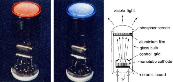
X-ray [Sugie 2001-2578] generators and microwave amplifiers [Brodie 1992-395]. Flat panel displays are one of the more lucrative applications of carbon nanotubes but are also the most technically complex. Nanotubes are at an advantage over liquid crystal displays since they have low power consumption, high brightness, a wide viewing angle, a fast response rate and a wide operating system. A 4.5 inch diode-type field emission display has been fabricated by
Samsung (Fig. 2-6), with SWNT stripes on the cathode and phosphor-coated ITO stripes on the anode running orthogonally to the cathode stripes [Choi 1999-399].
Cathode ray lighting elements with carbon nanotube materials as the field emitters have been fabricated by Ise Electronic Co. in Japan [Saito 1998-L348]. As illustrated in Fig. 2-7, these nanotube-based lighting elements have a triode-type design.
Fig. 2-6 A prototype 4.5 field emission display fabricated by Samsung using carbon nanotubes [Choi 1999-399].
Fig. 2-7 Demonstration of field emission light source using carbon nanotubes as the cathodes
(b) Nanometer sized device
Electronic circuits cannot continue to shrink by orders of magnitude and provide corresponding increases in computational power, unless radically different device materials, architectures, and assembly processes are developed. Dramatic recent advances have fueled speculation that nanotubes will be useful for downsizing circuit dimensions. Research toward nanoscopic CNT-FETs aims to replace the source-drain channel structure with a nanotube. A more radical approach is to construct entire electronic circuits from interconnected nanotubes. Because the electronic properties depend on helicity, it should be possible to produce a diode, for example, by grafting a metallic nanotube to a semiconducting nanotube. As shown in Fig. 2-8, Bachtold et al. [Bachtold 2001-1317] reported a nanotube transistor using integrated nanotubes which may lead to large scale integration.
Fig. 2-8 Nanoelectronic devices. (a) Schematic diagram for a CNT-FET. The semiconducting nanotube, which is on top of an insulating aluminum oxide layer, is connected at both ends to gold electrodes. (b) Scanning tunneling microscope (STM) picture of a SWNT field-effect transistor made using the design of (a) [Bachtold 2001-1317].
(c) Sensors
CNTs have some advantages for sensing applications such as their small size with larger surface; high sensitivity, fast response and good reversibility at room temperature enable them as a gas molecule sensor; enhanced electron transfer when used as electrodes in electrochemical reactions; and easy protein immobilization with retention of activity as potential biosensors are among some of the desirable applications. The main advantage of these sensors are the nanoscopic size of the nanotube sensing element and the corresponding nanoscopic size of the material required for a response [Baugham 2002-787].
The electrical resistivity of SWNTs has been found to change sensitively on exposure to gaseous ambients containing NO2, NH3, and O2. By monitoring this change the presence of
gases could be detected. Results showed are at least an order of magnitude faster than those currently available and that they could be operated at room temperature or at higher temperatures for sensing applications [Ajayan 2001-391].
(d) Probes
With extremely small sizes, high conductivity, high mechanical strength and flexibility (ability to easily bend elastically), nanotubes may ultimately become indispensable in their use as nanoprobes. The mechanical robustness of the nanotubes and the low buckling force increase the probe life along and minimizes damage during repeated hard crashes into substrates [Wang 2001-883]. The cylindrical shape and small tube diameter also allow for imaging in narrow deep crevices and improve resolution in comparison to conventional nanoprobes, especially for high sample feature heights [Hafner 1999-761]. Since MWNTs are conducting they can be used as scanning probes on microscope tips in instruments such as a STM, atomic force microscope (AFM) and electrostatic force microscopes (Fig. 2-9).
On an AFM tip they can be controlled like tweezers to pick up and release nanoscale structures. Nanoscopic tweezers have been made that are driven by the electrostatic interaction between two nanotubes on a probe tip [Kim 1999-2148]. They may be used as
nanoprobes for assembly. These uses may not have drastically impact of other commercial applications, however they increase the value of measurement systems for characterization and manipulation on the nanometer scale.
(e) Energy storage
Graphite, carbonaceous materials and carbon fiber electrodes have been used for decades in fuel cells, batteries and several other electrochemical applications. Carbon nanotubes are now being considered for energy storage and production because of their small dimensions, a smooth surface topology, and perfect surface specificity since only the graphite planes are exposed in their structure.
Fuel cells will most likely be the energy source of the future, for vehicles, local off-grid power supply, and power sources for small and handheld electronic devices. Pure MWNTs Fig. 2-9 Use of a MWNT as an AFM tip At the center of the VGCF is a MWNT which forms the tip. The VGCF provides a convenient and robust technique for mounting the MWNT probe for use in a scanning probe instrument [Ajayan 2001-391].
and MWNTs deposited with metal catalysts (Pd, Pt, Ag) have been used to electro-catalyze an oxygen reduction reaction, which is important for fuel cells [Britto 1999-154, Che 1998-346, Planeix
1994-7935]. It is seen from several studies that nanotubes could be excellent replacements for
conventional carbon-based electrodes.
The basic working mechanism of rechargeable lithium batteries is electrochemical intercalation and de-intercalation of lithium between two working electrodes. MWNTs consist of more than two graphitic sheets rolled into closed and concentric 1D cylinders. The graphitic sheets have an inter-planar spacing of ca. 0.34 nm, which allows the intercalation/deintercalation of Li ions. Several different approaches have been used to incorporate MWCNTs as the anode material in Li-ion batteries [Yang 2001-7, Yang 2005-347, Claye
2000-2845]. The MWNT-based batteries show reversible capacities of 80– 540 mAh g-1 and very
high irreversible capacities. As a result, there has been much recent effort devoted to improving these capacities and the Coulombic efficiency to meet the power requirements of microelectronic and telecommunication devices.
The area of hydrogen storage in CNTs remains active and controversial. Extraordinarily high and reversible hydrogen adsorption in SWNT containing materials [Dillon 1997-377, Chen-1999-91,
Liu 1999-1127, Nutenadel 1999-30] has been reported and has attracted considerable interest in both
academia and industry. However, many of these reports have not been independently verified. There is also a lack of understanding of the basic mechanism(s) of hydrogen storage in these materials.
(f) Photovoltaic application
Organic photovoltaic devices (OPVs) are fabricated from thin films of organic semiconductors, such as polymers and small-molecule compounds, and are typically on the order of 100 nm thick. Combining the physical and chemical characteristics of conjugated polymers with the high conductivity along the tube axis of CNTs provides a great deal of incentive to disperse CNTs into the photoactive layer in order to obtain more efficient OPV
devices [Miller 2006-133117, Ago 1999-1281, Miller 2006-123115, Miller 2007 -023105]. The interpenetrating bulk donor–acceptor heterojunction in these devices can achieve charge separation and collection because of the existence of a bicontinuous network. Along this network, electrons and holes can travel toward their respective contacts through the electron acceptor and the polymer hole donor. Photovoltaic efficiency enhancement is proposed to be due to the introduction of internal polymer/nanotube junctions within the polymer matrix. The high electric field at these junctions can split up the excitons, while the SWNT can act as a pathway for the electrons. Another benefit is that SWCNT films exhibit a high optical transparency in a broad spectral range from the UV-visual far into the near IR range. Only a few materials retain reasonable transparency in the infrared spectrum while maintaining transparency in the visible part of the spectrum as well as acceptable overall electrical conductivity, so CNTs could be used as a transparent electrode. SWCNT films are highly flexible, do not creep, do not crack after bending, theoretically have high thermal conductivities to tolerate heat dissipation, and have high radiation resistance.
Due to the simple fabrication process, low production cost, and high efficiency, there is significant interest in dye-sensitized solar cells (DSSCs). With recent progress in CNT development and fabrication [Kongkanand 2007-676, Jang 2004-9807, Lee 2007-513115], there is promise to use various CNT based nanocomposites and nanostructures to direct the flow of photogenerated electrons and assist in charge injection and extraction. To assist the electron transport to the collecting electrode surface in a DSSC, a popular concept is to utilize CNT networks as support to anchor light harvesting semiconductor particles. Other researchers fabricated DSSCs using the sol-gel method to obtain titanium dioxide coated MWNTs for use as an electrode. Because pristine MWNTs have a hydrophobic surface and poor dispersion stability, pretreatment was necessary for this application
2.3 Selective deposition methods for the nanostructures
(a) Patterning by photo- or electron-beam lithography
In most selective deposition process, the location of CNSs is defined by patterning the catalyst materials or substrates using photo- or electron-beam lithography. Growth of a single freestanding MWNTs on each nano-nickle dot was first proposed by Ren’s group. [Ren 1999-1086] As known in Fig. 2-10, they fabricated the array of individual MWNTs onto a grid of patterned nickel to investigate array of MWNTs for applications of flat panel field emission displays. Using the similar idea of constructing periodic arrays of nickel dots prepared by polystyrene nanosphere lithography was reported by Huang’s group. Patterned CNTs were fabricated by pre-patterning catalysts on the substrate depending on lithography technique. The idea of the substrate-dependent site-selective growth of aligned CNTs on the SiO2/Si was
reported by Zhang’s group by using the precursors of ferrosene and xylene, as shown in Fig. 2-11 [Zhang 2000-3764]. Later, the method continues to arrange into well-defined configuration in order to build integrated system by Wei’s group by using pre-patterning the SiO2/Si substrate [Wei 2000-3586].
Fig. 2-10 SEM micrographs showing growth of carbon nanotube obelisks on an array of submicron nickel dots [Ren 1999-1086].
(b) Template-based method
Porous structures such as zeolite [Hernadi 1996-416], anodic aluminum oxide (AAO) or porous Si are often used as the template for nanostructures. AAO has advantages of the uniform pore diameter, highly ordered pore arrangement, high packing density, low cost …are often used as templates, stencils, or masks, a number of approaches for fabricating a variety of nano-superstructures. The structure of the AAO consists of close-packed hexagonal cells, each with a straight pore channel perpendicular to the aluminum substrate and a thin Al2O3 barrier
layer lies adjacent to the aluminum substrate with a hemispherical, scalloped geometry at the pore bottom. The porous oxide growth consists of three stages that can be identified by the characteristic behavior of current versus time for potentiostatic anodization or potential versus time for galavanostatic anodization. These stages of pore formation are schematically shown in Fig. 2-12(a). When an anodic voltage is applied, the current decreases linearly with time, implying a linear increase in resistance or a linear growth of aluminum oxide on the surface of aluminum and high-resistance oxide (stage I). Tiny cracks appear at the oxide/electrolyte interface and they widen to form pores (stage II). Further anodization causes the pores to accelerate and attain a constant dissolution speed (stage III) [Thamide 2002-240].
Fig. 2-11 A SEM image of a patterned SiO2/Si substrate exposed to the precursor. Carbon
nanotubes have grown selectively on the SiO2 patterns, with no observable growth on the Si
The reactions involved in Al anodization process are described in Fig. 2-12(b). When aluminum is oxidized to alumina, the oxidation takes place at the entire metal/oxide interface, aluminum ions are formed due to charge transfer or electrochemical reaction:
− ++ →Al e Als 3 3 ) ( (2.8) The metal/oxide interface moves away from the interface of the electrolyte and the oxide was due to interaction of diffusing oxygen species with aluminum ions produced anodically at the Al2O3/Al interface: + − + + OH → Al O + H Al 3 3 2 3 2 3 (2.9) At the oxide/electrolyte interface, aluminum oxide grows according to the outward migration of aluminum ions (mainly by a place-exchange mechanism) and their reaction with oxygen-containing electrolyte species:
+ −
+ + OH → Al O + H
Al 3 3
2 3 2 3 (2.10) This aluminum oxide is also dissolved as a result of field-stimulated interaction of electrolyte species with the oxide surface:
O H Al H O Al 3 2 3 2 +6 + →2 + +3 (2.11) The oxide/electrolyte and metal/oxide interface are moving boundaries and the local electric field is the key variable along the interfaces that determines the reaction rate or speed of the interface [Li 1998-2470].
A number of researches have been reported that the geometric dimension and size of these pores are strongly related to the anodizing conditions (applied voltage, acid concentration of the electrolyte, and temperature). Most of these experimental data were obtained for sulfuric, oxalic, and phosphoric acids in the range of 0 < pH < 1 and with the applied voltage of 20–160 volts. Fig. 2-12(c) shows that the size of the pores or their interpore distance could be varied linearly with the applied voltage and the thickness of the porous
oxide film could be also controlled by the anodization time [Li 1998-6023].
(a) (b)
(c)
(c) Electrophoretic deposition (EPD)
EPD [Boccaccini 2006-3149] is a colloidal process wherein a direct current (DC) electric field is Fig. 2-12 (a) Three stages of AAO pore formation (b) The reactions involved in Al anodization process (c) The size of the pores or their interpore distance versus the applied voltage [Thamide 2002-240; Li 1998-2470; Li 1998-6023].
applied across a stable suspension of charged particles attracting them to an oppositely charged electrode. One electrode (cathode) consists of the substrate to coat, the anode being either an aluminum foil or stainless steel. The thickness of the coating depends on the distance between the two electrodes, the voltage (can vary from 10 to 300 V), the properties of the suspension (e.g. pH) and the duration.
(d) Self-assembly
Self-assembly is a term used to describe processes in which a disordered system of pre-existing components forms an organized structure or pattern as a consequence of specific, local interactions among the components themselves, without external direction. Self-assembly can be classified as either static or dynamic. In static self-assembly, the ordered state forms as a system approaches equilibrium, reducing its free energy. However in dynamic self-assembly, patterns of pre-existing components organized by specific local interactions are not commonly described as "self-assembled" by scientists in the associated disciplines. These structures are better described as "self-organized".
(e) Electroless plating
Electroless (autocatalytic) plating involves the presence of a chemical reducing agent in solution to reduce metallic ions to the metal state. There are no external electrodes present, but there is electric current (charge transfer) involved. Instead of an anode, the metal is supplied by the metal salt; replenishment is achieved by either adding salt or an external loop with an anode, of the corresponding metal, that has higher efficiency than the cathode. There is therefore, instead of a cathode to reduce the metal, a substrate serving as the cathode, while the electrons are provided by a reducing agent. The process takes place only on catalytic surfaces rather than throughout the solution (if the process is not properly controlled, the reduction can take place throughout the solution, possibly on particles of dust or of catalytic metals, with undesirable results).
the mere immersion in a suitable aqueous solution. A chemical reducing agent in solution supplies the electrons for converting metal ions to the metal form.
M 2+ + 2e - (supplied by reducing agent) catalytic (up) / surface (down) → M 0 (2-12) The important point is that the catalytic surface is the only place where this simplified reaction occurs. Once the deposition starts on a surface, the deposited metal must also be catalytic for the deposition to continue. The progress of electroless deposition is linear in time. As deposition progresses, islands are formed around these nucleation sites. These islands grow in size until they merge and a continuous film results. It was also established that the film mass thickness growth rate in electroless deposition is linear in time once film continuity has been reached. The mass thickness of a deposit is the deposited film’s volume pre unit area. This thickness factor refers to the total material deposited as a continuous film of even thickness, and it is compared to electrodeposition under conditions of constant current density.
(f) Electroplating
For the electroplating process an electrical current is used to coat a substrate or to fill a mould with a metal or an alloy on a conductive substrate. The substrate to be plated is the negative electrode, the cathode, as it is called. The positive electrode is the anode made from the material to be plated on the cathode. Anode and cathode are connected to an external power supply. The electrodes are immersed in a solution called electrolyte containing metallic ions. If a current is applied the ions will conduct the current. The positively charged ions are transported by the field lines to the cathode where they are reduced to metal by the electrons of the cathode. If the electrolyte contains metallic ions being different from the material of the anode an alloy will be deposit. At the cathode the chemical reaction is given as:
Mion + e - → M (2-13)
The anode dissolves and provides the metallic ions. The dissolution reaction is as follows: M → Mion + e - (2-14)
solutions):
at the cathode: 2H ++ 2e - → H2 (2-15)
at the anode: H2O → 1/2 O2 + 2H+ + 2e - (2-16)
The hydrogen gas is an unfavourable product because it is incorporated in the deposited material and reduces its quality.
2.4 Fabrication methods for the oriented CNSs
(a) Aligned growth under external forces
Directed assembly under external forces such as by flow and electric fields[Huang 2003-1651,
Chen 2001-3714, Zhang 2001-3155]. In particular, the approach using electric-field assisted assembly has
been actively explored as a viable integration strategy for lateral alignment of CNTs. The use of electric field can be applied postgrowth [Krupke 2003-1019, Nagahara, I. 2002-3826]. or during growth
[Ural 2002-3464, Joselevich 2002-1137]. In the Fig. 2-13(a), the growth is defined by patterning the
catalyst nanoparticles, while the direction of growth is defined by a local electric field parallel to the substrate. Statistical analysis of the nanotube angular distribution indicates that field-directed growth can discriminate between metallic and semiconducting nanotubes during their formation [Joselevich 2002-1137].
(b) Template approaches
Another method of aligned growth of nanostructures is to use a nanoporous template. In this method, porous alumina produced in an aluminum anodization process is used as a template for nanotube growth. The anodic alumina has a porous structure with nanopores (30–50 nm) self-organized in a hexagonal pattern. Catalyst is electrodeposited into the nanopores and then nanotubes are synthesized by CVD. The porous template may be etched away after nanotube synthesis. An array of aligned nanotubes prepared using this fabrication process is shown in Fig. 2-13(b) [Li, 1999-367].
(a) (b)
(c) (d)
(e)
(c) Crowding effect
Most frequently found in the literature are nanotubes grown in a very dense organization with vertical alignment due to the crowding effect. Fan et al.[Fan 1999-512] used porous silicon Fig. 2-13 Approaches to carbon nanotube organization: (a) Aligned growth under external forces, (b) Template approaches, (c) Crowding effect,(d) Postgrowth aligned deposition from liquid dispersions, and (e) Epitaxial approaches [Joselevich 2002-1137; Li, 1999-367; Fan 1999-512; Ago 2005-433;
substrates with evaporated iron catalyst pattern to produce nanotube blocks by thermal CVD that grew perpendicular to the substrate. As shown in Fig. 2-13(c), the high density of nanotubes within each block confined the nearest neighbors and attracted the outermost nanotubes to their neighbors via van der Walls forces, resulting in the oriented growth.
(d) Postgrowth aligned deposition from liquid dispersions
Several approaches have been explored to laterally align CNTs such as controlled
directed deposition through chemical modification of the surfaces of nanotubes or substrates
[Burghard 1998-584, Meitl 2004-1643]. Postgrowth aligned deposition from liquid dispersions at specific
locations and directions on the surface, by means of chemical modifications on either or both surface and nanotubes under external forces generated by flow, magnetic, or electric fields, and surface acoustic waves. However, the dispersion of nanotubes in liquid is difficult, normally requiring sonication or acid treatment. Moreover, the intrinsic electrical and mechanical properties of the SWNTs are often damaged by both sonication and chemical modification.
Poulin and co-workers have made important progress in this direction through their flow-induced alignment method [Vigolo, 2000-290]. The method starts with a macroscopically stable nanotube suspension, which is made by dispersing SWNTs in an aqueous solution of sodium dodecyl sulfate (SDS). As shown in Fig. 2-13(d), the suspension is injected through a 0.5-mm-diameter syringe needle into a 5 wt% polyvinylalcohol solution, which is in a cylindrical container rotated at speeds ranging from 30 to 150 rpm. CNT alignment induced by the shear or elongational flow takes place at the tip of the needle. The alignment is maintained by the polyvinylalcohol solution because it allows the nanotubes to rapidly stick together as they emerge from the needle. Long ribbons (Fig. 2-13(d)) are thus formed in the solution and SWNT bundles are preferentially aligned along the main axis of the ribbons.
(e) Epitaxial approaches
(lattice-directed epitaxy), atomic steps (ledgedirected epitaxy), and nanofacets (graphoepitaxy) on single-crystal surfaces [Ago 2005-433, Ismach 2006-1706].
2.5 Analysis methods of the CNSs
In nanoscale science and technology, the characterization of products represents a persistent problem and the experimental techniques that have been used for the qualitative and quantitative characterization of CNSs in the current literature are presented briefly.
2.5.1 Morphologies, and lattice image analyses
High-resolution microscopes are indispensable instruments for the characterization of CNSs due to their ability to directly visualize the outcome of the experiments. Transmission electron microscopy (TEM), scanning electron microscopy (SEM), and atomic force microscopy (AFM) have been the most widely employed techniques. In TEM, a thin sample (normally several tens of nanometers or less in thickness) is required to ensure that an accelerated electron beam can pass through it. The sample size is very small, normally no more than 50 mm. The focused ion beam, also known as FIB, is also commonly used to prepare samples for the transmission electron microscope. The nanometer-scale resolution of the FIB allows the exact thin region to be chosen. This is vital, for example, in integrated circuit failure analysis. If a particular transistor out of several million on a chip is bad, the only tool capable of preparing an electron microscope sample of that single transistor is the FIB. However, the drawback to FIB sample preparation is the surface damage and implantation, which produces noticeable effects when using techniques such as high-resolution “lattice imaging” TEM or electron energy loss spectroscopy. This damaged layer can be minimized by FIB milling with lower voltages or by further milling with a low voltage argon ion beam after completion of the FIB process. In SEM, there is no limit on
![Fig. 2-1 Eight allotropes of carbon: (a) Diamond, (b) Graphite, (c) Lonsdaleite, (d) C 60 , (e) C 540 , (f) C 70 , (g) Amorphous carbon, and (h) Single-walled carbon nanotube [http://en.wikipedia]](https://thumb-ap.123doks.com/thumbv2/9libinfo/8744029.204582/19.892.157.791.539.1083/allotropes-diamond-graphite-lonsdaleite-amorphous-single-nanotube-wikipedia.webp)
![Fig. 2-2 Ternary ‘phase’ diagram of carbon allotropes. P/H corresponds to the ratio of pentagonal/hexagonal rings [Heinmann 1997-1654] .](https://thumb-ap.123doks.com/thumbv2/9libinfo/8744029.204582/21.892.273.716.118.498/ternary-diagram-carbon-allotropes-corresponds-pentagonal-hexagonal-heinmann.webp)
![Fig. 2-10 SEM micrographs showing growth of carbon nanotube obelisks on an array of submicron nickel dots [Ren 1999-1086]](https://thumb-ap.123doks.com/thumbv2/9libinfo/8744029.204582/33.892.125.808.525.1042/micrographs-showing-growth-carbon-nanotube-obelisks-submicron-nickel.webp)