高介電氧化鋁閘極於下世代深次微米技術的應用
High-K Al
2O
3gate dielectrics on next generation VLSI technology
計畫編號:NSC 89-2215-E-009-099
執行期限:89 年 8 月 1 日至 90 年 7 月 31 日
主持人:
荊鳳德學生:
陳晞白交通大學電子工程系
一、中文摘要 藉由直接氧化沈積在矽晶片上的鋁 膜,可以成長出氧化鋁薄膜。K 值為 8.5 的 21Å 及 36 Å 氧化鋁具有等效氧化層厚 度約 9.6Å 及 16.5Å。21 Å 氧化鋁在 1V 的 偏壓下漏電流密度為 0.4 A/cm2 ,介面缺陷 密度約在 2~3×10¹¹ eV-1 /cm2 ,而 3,600 秒 2.5V 的偏壓下,仍有很好的可靠度,以上 證明了氧化鋁薄膜具有好的介電特性。 關鍵詞:閘極介電質、氧化鋁、介電性質 A b s t r a c tWe have investigated the gate dielectric integrity of Al2O3 formed by a simple
process using direct oxidizing the deposit Al on Si. The 21Å and 36 Å Al2O3 gate
dielectric have a K value of 8.5 that is equivalent to an oxide thickness of 9.6Å and 16.5Å. Good dielectric integrity is evidenced by the very low leakage current density of 0.4 A/cm2 at 1V for 21 Å Al2O3, low
interface-trap density of 2~3×10¹¹ eV-1/cm2, and good reliability measured by the small SILC after 2.5V stress for 3,600s.
K e y w o r d s : gate dielectric, Al2O3,
dielectric integrity 二、緣由與目的
By continuously scaling down the CMOS technology, ultra-thin gate dielectrics with equivalent oxide thickness below 10-15Å will soon be needed for sub-0.1µm devices. Although recently Si3N4 gate dielectric has
been studied extensively for replacing thermal SiO2 [1]-[2], the marginal
improvement is due to the relatively lower K and slightly higher leakage current. Thus, Si3N4 might be used only for one or two
generations of device scaling. Therefore, the search for alternative gate dielectric with higher dielectric constant than Si3N4 is
urgently required for future VLSI generation [1]-[4]. In addition to high K value, this alternative gate dielectric must also have low leakage current, good interface property, good thermal stability, small stress-induced leakage current (SILC), good reliability, and process compatibility to existing VLSI technology. Recently, we have developed the Al2O3
material [5]-[6] as another candidate for high K gate dielectric that has a K value of ~ 9 higher than Si3N4. Further, the Al2O3
gate dielectric can satisfy almost all the above requirement except that the relatively high interface-trap density and slightly large dielectric thickness [8]. In this paper, we have further improved the dielectric integrity of Al2O3. We have
achieved a low leakage current density of 10-6 A/cm2 at 1V with an equivalent oxide thickness of 18Å and 0.4 A/cm2 at 1V for 21 Å with an equivalent oxide thickness of 9.6Å Al2O3. The interface-trap density is about
2~3 × 10¹¹ eV-1/cm2. Good reliability is evidenced by the small SILC after 2.5V stress for 3,600s.
Standard p-type Si wafers with resistivity of ~10 Ω–cm were used in this study. After device isolation, amorphous Al layer is deposited by ultra-high vacuum molecular beam epitaxy (MBE) system. A HF-vapor passivation [7]-[8] is used to reduce the desorption temperature of native oxide in MBE before Al deposition. The deposited Al is first oxidized at a temperature of 500oC for 1 hour by oxygen followed by a 900oC furnace annealing for 30 min in nitrogen ambient. In comparison with chemical-vapor deposited (CVD) or sputtering deposited Al2O3, the direct
oxidation process is simpler and may have better gate dielectric property because it is well known that thermal SiO2 has better
integrity than CVD SiO2. MOS devices
were formed after a 3000Å poly-Si deposition and subsequent patterning.
四、結果與討論
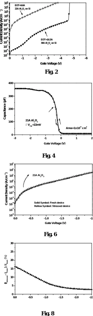
In order to get accurate K and EOT, the oxide thickness is carefully examined by both ellipsometer and TEM in Fig. 1. The very uniform oxide and smooth interface are due to native oxide free surface and high thermal stability as contact with Si. Fig. 2 shows the J-V characteristics of 21Å and 36Å Al2O3 capacitor. Good
Flower-Nordheim (F-N) tunneling behavior is observed that suggests relatively low defect concentration. A breakdown electric voltage of ~4V for 36Å Al2O3 is measured that is
high enough for sub-µm devices application. A low leakage current density of 10-6 A/cm2 is measured at 1V; to our best knowledge, this is the lowest reported value for high K gate dielectric with an equivalent oxide thickness of 16.5Å. Fig. 3 shows the cumulative values for 21Å Al2O3, and
leakage current of 0.4 A/cm2 are obtained. The related dielectric constant is measured by C-V characteristics in Fig. 4, and a value of 8.5 is obtained.
In order to apply Al2O3 gate dielectric to
current CMOS technology, good
interface-trap density is unavailable because it is directly related to low frequency noise of MOS transistor [9]. We have therefore measured the interface-trap density for the 36Å Al2O3 that is obtained from the
quasi-static and high frequency C-V curves. Fig. 5 shows the measured interface-trap density. A minimum interface-trap density of 2~3× 10¹⁰ eV-1/cm2 is obtained that is close to conventional thermal SiO2. It is also
important to notice that further reduction of interface-trap density is possible using forming gas annealing. However, the weak hydrogen-Si bond at interface may degrade the device reliability [10]. The lower interface-trap density for 36Å Al2O3 than our
previous work may be due to the thinner thickness for oxygen penetration and additional SiO2 formed beneath Al2O3. This
is evidenced by the slightly lower K value as compared to our previous report.
Gate dielectric reliability is another important factor for practical VLSI application. We have measured Al2O3
reliability under a constant voltage stress of 2.5V for 3,600s. Fig. 6 plots the SILC to show the difference between fresh and stressed devices, and Fig. 7 is the current variation during stress. No soft breakdown can be found even after a charge injection of 2.5 C/cm2. Excellent reliability is evidenced from the tiny current change during stress and very small SILC after stress as shown in Fig. 8. The excellent SILC resistance may be important for certain device application such as flash memory. Therefore, the Al2O3 gate
dielectric is suitable for continuous operation at VLSI generations of 2.5V and beyond.
五、計畫成果自評
We have studied the gate dielectric integrity of Al2O3 formed by direct oxidizing
the deposit Al on Si. The 38Å Al2O3 gate
dielectric have a K value of 8.5 that is equivalent to an oxide thickness of 18Å.
Good dielectric integrity is evidenced by the very low leakage current density of 10-6 A/cm2 at 1V, low interface-trap density of 2~3 × 10¹¹ eV-1/cm2, and good reliability measured by the small SILC after 2.5V stress for 3,600s. In addition to high K value, these dielectric properties are very close to conventional thermal SiO2.
六、參考文獻
[1] S.C. Song, H.F. Luan, Y.Y. Chen, M. Gardner, J. Fulford, M. Allen, and D. L.
Kwong, “Ultra thin (<20Å) CVD Si3N4 gate
dielectric for deep-sub-micron CMOS devices,” in IEDM Tech. Dig., 1998, pp. 373-376.
[2] H.-H. Tseng, D. L. O'Meara, P. J. Tobin, V. S. Wang, X. Guo, R. Hegde, I. Y. Yang, P. Gilbert, R. Cotton, and L. Hebert, “Reduced gate leakage current and boron
penetration of 0.18 µm 1.5 V MOSFETs
using integrated RTCVD oxynitride gate dielectric,” in IEDM Tech. Dig., 1998, pp. 793-796.
[3] X. Guo, T. P. Ma, T. Tamagawa, and B.L
Halpern, “High quality ultra-thin
TiO2/Si3N4 gate dielectric for giga scale
MOS technology,” in IEDM Tech. Dig., 1998, pp. 377-380.
[4] C. Hobbs, R. Hegde, B. Maiti, H. Tseng, D. Gilmer, P. Tobin, O. Adetutu, F. Huang, D.
Weddington, R. Nagabushnam, D.
O’Meara, K. Reid, L. La, L. Grove and M. Rossow, “Sub-quarter micron CMOS
process for TiN-gate MOSFETs with TiO2
gate dielectric formed by titanium oxidation,” in Symp. on VLSI Tech.,1999, pp. 133-134.
[5] C. C. Liao, A. Chin,and C. Tsai, “Electrical
Characterization of Al2O3 on Si from
MBE-grown AlAs and Al ,” 10th International
Conf. on Molecular Beam Epitaxy (MBE),August 1998; J. Crystal Growth,
201/202, 652 (1999).
[6] A. Chin, C. C. Liao, C. H. Lu, W. J. Chen, and C. Tsai, “Device and Reliability of
High-K Al2O3 Gate Dielectric with Good
Mobility and Low Dit,” in Symp. on VLSI
Tech., 1999, pp. 135-136.
[7] Y. H. Wu, W. J. Chen, S. L. Chang, A. Chin, S. Gwo, and C. Tsai, “Improved Electrical
characteristics of CoSi2 Using HF-Vapor
Pretreatment,” IEEE Electron Device Lett., vol. 20, no. 5, pp. 200-202 (1999).
[8] A. Chin, W. J. Chen, T. Chang, R. H. Kao, B. C. Lin, C. Tsai, and J. C.-M. Huang, “Thin Oxides with in-situ Native Oxide Removal,” IEEE Electron Device Lett. vol. 18, no. 9, pp. 417-419 (1997).
[9] H. Kimijima, T. Ohguro, B. Evans, B. Acker, John. Bloom, H. Mabuchi, D. L. Kwong, E. Morifuji, T. Yoshitomi, H. S. Momose, M. Kinugawa, Y. Katsumata, and H. Iwai “Improvement of I/f noise by using VHP (Vertical High Pressure) oxynitride gate insulator for deep-sub micron RF and analog CMOS,” in Symp. on VLSI
Tech.,1999, pp. 119-120.
[10] B. C. Lin, Y. C. Cheng, A. Chin, T. Wang, and C. Tsai, “The Deuterium Effect on SILC,” Extended Abstract in Int. Solid
State & Materials, 110 (1998).
F i g u r e C a p t i o n s :
Fig. 1. Cross-section TEM of 21Å Al2O3. Very
smooth interface is due to the high thermal stability and native oxide free surface.
Fig. 2. J-V characteristics for 21Å and 36Å Al2O3
capacitors.
Fig. 3. Cumulative distribution of leakage current and for 21Å Al2O3 gate
dielectrics.
Fig. 4. Hysteresis curves for 21Å Al2O3 gate
dielectrics.
Fig. 5. Interface state density of Al2O3 on Si.
Min Dit of 3x10¹⁰ eV-1/cm2 is obtained for
both dielectrics and close to SiO2/Si.
Fig. 6. Stress induced leakage current and
current variation for Al2O3 under
-2.5V for 1hr.
Fig. 7. Time evolution of Ig under -2.5V for 1hr
with Qinj of 1.5x10⁵ C/cm2 for Al2O3.
Fig. 8. The leakage current difference for 21Å Al2O3.
0 -1 -2 -3 -4 -5 -6 10-9 10-8 10-7 10-6 10-5 10-4 10-3 10-2 10-1 100 101 102 103 EOT=16.5A 36A Al 2O3 on Si EOT=9.6A 21A Al2O3 on Si Gate Voltage (V)
Current Density (A/cm
2 ) -3 -2 -1 0 1 2 0 100 200 300 400 Area=1x10⁻⁴ cm2 21A Al2O3 △VFB=22mV Gate Voltage (V) Capacitance (pF) -0.6 -0.5 -0.4 -0.3 -0.2 -0.1 0.0 0.1 0.2 1010 1011 1012
EOT=16.5A 36A Al2O3/Si
Dit (ev -1 /cm 2 ) Energy (ev) 0 500 1000 1500 2000 2500 3000 3500 0.1 1 10 100 Time (second)
Current Density (A/cm
2 )
21A Al2O3 CVS under -2.5V for 3600sec
0.0 -0.5 -1.0 -1.5 -2.0 -2.5 10-6 10-5 10-4 10-3 10-2 10-1 100 101 102 103
Current Density (A/cm
2 )
21A Al2O3
Gate Voltage (V)
Solid Symbol: Fresh device Hollow Symbol: Stressed device
0.1 1 0 20 40 60 80 100 Cumulative Failure (%)
Leakage Current Density @ -1V (A/cm2
) Al2O3 21A 0.0 -0.5 -1.0 -1.5 -2.0 -2.5 0 5 10 15 20 25 30 (Istressed - I Fresh ) / I fresh (%) Fig. 2 Fig. 1 Fig. 4 Fig. 3 Fig. 6 Fig. 5 Fig. 8 Fig. 7 10nm G l u e S i A l2O3 Fig. 1