Characterization ofA High Quality and UVTransparent
PECVD Silicon Nitride Film
for
Non-Volatile Memory Applications
C.K.Wang, *T.L.ying, *C.S.Wei, *L.M.Liu, H.C.Cheng and *MSLjII
Department ofElectronics Engineering and Institute of Electronics, National Chiao Tung University. Taiwan, R.O.C.
*Taiwan
Semiconductor Manufacturing Company,
No.121, Park Ave. 3 Science Based Industrial Park Hsin-Chu. Taiwan, R.O.C.
ABSTRACT
A high quality and UV-transparent plasma enhanced chemical vapor deposition (PECVD) silicon nitride film is well developed to form passivation layer for non-volatile momery devices. The dependence of the film properties on process parameters has been studied by factorial designed experiments. The deposition rate, uniformity, stress, refractive index, wet etching rate, density, step coverage and UV-transmittance are the items used to evaluate the film properties. Rutherfold backside scattering (RBS) and hydrogen forward scattering (HFS) are used to measure the film
composition and total hydrogen composition, respectively. Comparing to the
tranditional PECVD nitride (PE-SiN) film known to have tensile stress and opacity to ultra-violet light (UV light), the developed PE-SiN film with very low compressive stress (< 1 E9 dynes/cm*2) and excellent UV-transmittance (>70% for 1 .6um-thick film) can be achieved. The developed film has higher density, lower hydrogen content
and high N/Si inside film. Based on RBSIHFS, UV-transmittance and Fourier
Transform Infrared Spectrum (FTIR) results, the material and optical properties of the
developed PE-SiN film is well investigated. This developed PE-SiN film is
successfully applied to EPROM devices, and very good electrical and reliability performances have been demonstrated.
Keywords PE-SiN, UV-transmittance, EPROM
282/SPIE Vol. 2335
2. INTRODUCTION
Silicon nitride films have been widely used in semiconductor device fabriaction for various purposes. For the application of passivation layer, the silicon nitride film is used to protect underlying device structures. PECVD approach is usually adopted to minimize backend thermal process. Amorphous silicon nitride (a-SiN:H) is one of the popular films for passivation. However, conventional PECVD silicon nitride film possesses relatively high internal stress. The excessive tensile or compressive stress easily causes cracking or peeling of the deposited film. Therefore, PECVD silicon nitride is often used together with PECVD silicon dioxide (PE-OX), TEOS (tetraethoxysilane) based silicon dioxide (PE-TEOS) or phosphorus doped silicon glass (PSG) to form passivation layer. On the other hand, the opacity to ultra-violet light (LIV light) ofconventional PE-SiN film also limits the application for
non-volatile devices such as EPROM. PE-OX, PE-TEOS and PSG are the general
passivation layers used for non-volatile, memory devices such as EPROM/FLASH EPROM/EEPROM. However, these films can not effectively block the penetration of moisture and mobile ions. As a result of this, more reliability issues are induced by using these oxide-based films.
In this paper, one high quality and UV-transparent PECVD silicon nitride film is well developed. The film stress can be controlled below 1E9 dynes/cm*2 compressive. Dense film characteristics is identified by pin-hole test. Meanwhile, the
UV-transmittance is comparable to that of PE-OX. The physical properties are
detailedly characterized by means of factorial design experiments to understand the correlations between various process parameters (temperature, pressure, RF power, spacing and SiH4INH3 flow ratio) and system responses (deposition rate, uniformity,
stress, refractive index, wet etching rate, density, step coverage and
UV-transmittance).' The film composition and total hydrogen concentration are measured by Rutherfold backside scattering (RBS) and hydrogen forward scattering (HFS), respectively. From the RBSIHFS, UV-transmittance and Fourier Transform Infrared Spectrum (FTIR) results, the optical properties of this developed PE-SiN film is investigated as well. Finally, the implementation of this PE-SiN film into EPROM
devices is performed Good electrical performance, device reliability and
3. EXPERIMENT
. ThePESiN films descriled in this paper have been deposited in a parallel
plate RF plasma enhanced CVD reactor at 400C and at a total pressure of 5 ton. The RF frequency is 13.56 MHz. A gas mixture of SiH4INH3IN2 was used as reactant gas. Factorial design experiements are conducted to characterize the deposition process.
Film stress at room temperature was calculated from wafer curvature. The refractive index is measured with an ellipsometer. The step coverage was observed with SEM. For pin-hole decoration, KOH solution was used. Regarding UV4ight transmission, the developed PE-SiN films were deposited on quartz wafers and measured in UV-2000 spectrometer. The UV-erasability was analyzed by monitoring the reduction of threshold voltage with erase time. For device reliability evaluation, high temperature baking and pressure cooking tests were performed.
4. RESULTS AND DISCUSSIONS
Table 1 shows the correlation between process parameters and output responses. The chamber pressure, RF power input, electrode spacing and SiH4INH3 gas flow ratio are critical process parameters for deposition rate. The SiH4INH3 gas flow ratio expresses significantly positive effect; deposition rate increases with SiH4INH3 flow ratio. On the other hand, chamber pressure, RF power input and electrode all show negative effect on deposition rate. For uniformity response, the electrode spacing is the only significant factor. There are two influential factors observed for film stress. One is the SiH4/NH3 gas flow ratio which shows a positive effect. This indicates that as the ratio increases the stress tends to be tensile. The other factor, the RF power input, shows a negative effect on film stress. It is necessary to pay more attention that stress is extremely sensitive to RF power. As for refractive index, it can be affected by chamber pressure, electrode spacing and SiH4INH3 gas flow ratio. As for film density, the dominated process parameter is RF power. Finally, the UV-transmittance is more related to chamber pressure and SiH4/NH3 gas flow ratio. The pressure has a significant positive effect to UV-transmittance; on the contrary, the SiH4INH3 ratio shows a drastically negative effect.
For the application of passivation layer of non-volatile memory devices, the low compressive film stress and good UV-transmittance are required. As shown
in figure 1, the dependence of film stress on RF power is characterized.
Apparently, low compressive stress less than 1E9 dynes/cm*2 can be obtained by properly adjusting RF power input. It is obviously that the film stress is very sensitive to RF power. The proposed explanation is that the RF power input dominates the ion bombardment in plasma CVD system. More ion bombardment is achieved by raising
power input. Denser film is therefore resulted and the stress tends to be compressive, due to the incorporation of bombarding ions in the film. For the change of every one watt in RF power, around 1E8 dynes/cm*2 stress shift is observed.
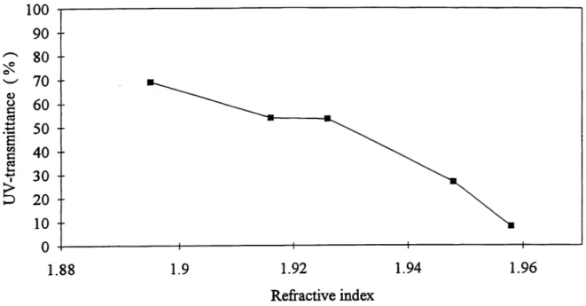
The optical properties of developed PE-SiN film was investigated by
correlating the UV-transmission with refractive index, film density and film
composition. As shown in figure 3, the UV4ransmittance degrades with increasing refractive index. For refractive index higher than 1 .93, the UV-transmission of
PE-SiN film decreases drastically. This is the reason why tranditional PE-PE-SiN with refractive index around 2.00 shows UV-opacity. The UV-transmittance was also
correlated to film density. As shown in figure 3, denser film achieves higher
transmission performance. The increase of UV-transmittance with the N/Si ratio is expressed in figure 4. This is because that a-SiN:H films with lower N/Si ratio have the microstructure closer to that of a-Si:H. The energy band gap is so narrow that it absorbs most of the incident UV-light. On the contrary, films with higher N/Si ratio have microstructure closer to that of high energy n-phase Si3N4 and hense possess better UV-transparency.2'3'4 The denser film generally has tighter bonding, therefore results in larger energy band gap and good UV-tranparency.
From the analysis of hydrogen forward scattering (HFS), the hydrogen content ofdeveloped PE-SiN film is about 25%lowerthan that oftranditional PE-SiN film. From the FTIR spectra of the developed PE-SiN before and after a 30 minute annealing at 410C, we observed larger change in the N-H peak than that of the Si-H peak. Similar observation has also been reported.5'6
The device performance of EPROM processed with developed PE-SiN as
passivation layer showed comparable result to that of EPROM with PE-OX
passivation. To study the erasability of UV-light, a 1 .6um-thick developed PE-SiN film was deposited on EPROM device wafers. One wafer with O.7um PE-OX film was used as a reference. On initially programmed devices, the threshold voltage (Vt)
was measured before and after a UV-light exposure (
intensity of 70 mw/cm*2,wavelength of 254nm). The erasability was evaluated from the relationship between Vt and exposure time. The two curves of 1 .6um developed PE-SiN and O.7um PE-OX films are shown in figure 5. They are nearly overlap with each other, indicating comparable UV-transmittance between the two films. The charge retention tests on EPROM devices had also been conducted. The Vt drop of a programmed EPROM cell after a 26 hours, 250C oven baking is shown in figure 6. The Vt drop of device wafers with developed PE-SiN are smaller than those with PE-OX. The pressure cooking test was performed at 121 C, 30 psia for 48 hours. The experimental results shown in figure 7 indicate that the use of developed PE-SiN as passivation layer can effectively block the attack of moisture.
5. CONCLUSIONS
A high quality and UV-transparent PECVD silicon nitride film has been developed and characterized as a passivation layer for non-volatile devices. Low compressive stress of PE-SiN film is easily controlled by adjusting BY power and good UV-transmittance is achieved by decreasing SiH4INH3 gas flow ratio. The
relationship of UV-transmission and refractive index, film density and film
composition is characterized as well. With the implementation of the developed PE-SiN film into EPROM devices, good UV-erasability and charge retention results are demonstrated.
6. ACKNOWLEDGMENTS
The authors would like to thank Dr. C.S. Lo for his support on device performance measurement. The useful discussions on experimental design and data analysis from Dr. C.S. Yoo are also greatly appreciated.
7. REFERENCES
1. C.S. Yoo and A.G. Dixon, The solid Films, 135, Vol. 167 (1989)
2. A. Morimoto, Y. Tsujimura, M. Kumeda and T. Shimizu, Japanese Journal of Applied Physics Vol. 24, No 11, November (1985) pp. 1394-1398
3. K. Maeda and I. Umezu, J. Appl. Phys. 70(5), 1 September (1991) pp. 2745-2754 4. Z. Yin and F.W. Smith, Phys. Rev., B42 (1990) pp. 3658-3664
5. E.A. Davis, N. Piggins and S.C. Bayliss, J. Phys. C: Solid State Phys. 20(1987) pp. 4415-4427
6. Z. Yin and F.W. Smith, Phys. Review B42 (1990) pp. 3666-3675
Temperaturel Pressure I RF power lElectrode spacing SiH4INH3 flow ratio
Deposition rate (A/mm) 0 -- - - +++
Uniformity (%)
0
0 0 -- 0Stress (dynes/cm*2) 0 0 --- 0 +
Refractive index 0 -- 0 - +
BOE etching rate (A/mm) 0 + 0 0 0
Density (g/cm*3) 0
0
+++ 0 -Step coverage (%) 0 +0
0 0 UV-transmittance (%) 0 +++ + 0 ---20 100
-50 420 Table 1: The relationship between process parameters and system responses+
:positive effect - negativeeffect 0 nearly no effect (The number of symbol represents the degree of sensitivity)*
C.) C)-20
-30 C)-40
360 370 380 390 400 410 R.F power (watt)Refractive index
Figure 2 : The correlation of UV..transmittance and refractive index. The deposited PESiN thickness is 1 6000A.
Density(g/cm*3)
Figure 3 The relationship between UV-transmittance and film density. The deposited thickness is 16000A.
1.9 1.92 1.94 1.96 100 90 80 70 60
.50
Er30
20
10 0 1.88100 —
90 70 20 100—
2.6 288/ SPIE Vol. 2335 2.65 2.7 2.75 2.8 2.85 2.9 2.95 3100 90
80
s...' 70 C.).50
E (12i30
20 10o
1.1 1.2N/Si Ratio
1.8 1.9Figure 4 The relationship of UV4ransmittance versus film composition (N/Si ratio). The deposited PE-SiN thickness is 16000A.
Time (sec)
•-— 16K UV-SiN
—s)-— 7K PE-OX
Figure 5 TheUV-erasability of developed PE-SiN (16000A) and PE-OX (7000A) was evaluated by monitoring the reduction of threshold voltage (Vt) with erase time.
1.3 1.4 1.5 1.6 1.7 V t V 0 1 t 1— : —i F
ó 10
20 30 40 50 60 70 80 90 1Ô0 110 120 130 140 150 160 170 180 190 200V t D
r
0 p m V Vt
D r 0 p m V 290/SPIEVol. 2335 • 16K UV—SiN —0— 7K PE—OXFigure6 : Charge retention test by measuring the Vt drop of a programmed
EPROM cell after 250C oven baking for 26 hours.
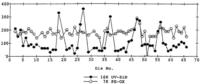
Die No.
_____- 16K UV—SiN
—0— 7K PE—OX
Figure 7 : Charge retention test by measuring the Vt drop after 121C, 30 psia pressure cooking for 48 hours.
65 Die No. 1 -t 1 I