IEEE ELECTRON DEVICE LETTERS, VOL. 31, NO. 12, DECEMBER 2010 1413
Analysis of Degradation Mechanism in SONOS-TFT
Under Hot-Carrier Operation
Te-Chih Chen, Ting-Chang Chang, Shih-Ching Chen, Tien-Yu Hsieh, Fu-Yen Jian, Chia-Sheng Lin,
Hung-Wei Li, Ming-Hsien Lee, Jim-Shone Chen, and Ching-Chieh Shih
Abstract—This letter investigates the degradation mechanism of
polycrystalline silicon thin-film transistors with a silicon–oxide– nitride–oxide–silicon structure underOFF-state stress. During the electrical stress, the hot hole generated from band-to-band tun-neling process will inject into gate dielectric, and the significant
ON-state degradation (more than 1 order) indicates that the inter-face states are accompanied with hot-hole injection. In addition, the asymmetric I–V characteristics indicate that the interface states are located near the drain side. Moreover, the ISE-TCAD simulation tool was utilized to model the degradation mechanism and analyze trap states distribution. Although both the vertical and lateral electrical fields are factors for degradation and hot-hole injection, the degradation is mainly affected by the lateral electrical field over a critical point.
Index Terms—Hot carriers, nonvolatile memory, thin-film
tran-sistors (TFTs).
I. INTRODUCTION
R
ECENTLY, significant advances have been made in system-on-panel (SOP) display technology with high-performance polycrystalline silicon thin-film transistors (poly-Si TFTs) designed as functional controller and memory devices [1]. Unlike conventional nonvolatile floating gate memory, silicon-oxide-nitride-oxide-silicon (SONOS)-type memory hasManuscript received August 3, 2010; revised September 5, 2010; accepted September 12, 2010. Date of publication November 1, 2010; date of current ver-sion November 24, 2010. This work was supported in part by the National Sci-ence Council of the Republic of China under Contracts NSC-98-3114-M-110-001 and NSC-97-2112-M-110-009-MY3, and part of the work was performed at AU Optronics Corporation. The review of this letter was arranged by Editor T. San.
T.-C. Chen, S.-C. Chen, and T.-Y. Hsieh are with the Department of Physics, National Sun Yat-Sen University, Kaohsiung 80424, Taiwan (e-mail: a49136@ yahoo.com.tw; [email protected]; [email protected]). T.-C. Chang is with the Department of Physics, National Sun Yat-Sen Uni-versity, Kaohsiung 80424, Taiwan, and also with the Center for Nanoscience and Nanotechnology and Department of Electro-Optical Engineering, Na-tional Sun Yat-Sen University, Kaohsiung 804, Taiwan (e-mail: tcchang@mail. phys.nsysu.edu.tw).
F.-Y. Jian is with the Department of Electro-Optical Engineering, National Sun Yat-Sen University, Kaohsiung 804, Taiwan (e-mail: [email protected]).
C.-S. Lin is with the Department of Electrical Engineering, National Sun Yat-Sen University, Kaohsiung 804, Taiwan (e-mail: [email protected]).
H.-W. Li is with the Department of Photonics and Institute of Electro-Optical Engineering, National Chiao Tung University, Hsinchu 30050, Taiwan (e-mail: [email protected]).
M.-H. Lee, J.-S. Chen, and C.-C. Shih are with the AU Optron-ics Corporation, Hsinchu 30078, Taiwan (e-mail: [email protected]; [email protected]; [email protected]).
Color versions of one or more of the figures in this letter are available online at http://ieeexplore.ieee.org.
Digital Object Identifier 10.1109/LED.2010.2079912
become a promising candidate for SOP applications because it is fully compatible with poly-Si TFTs processes [2], [3].
The poly-TFTs with oxide-nitride-oxide (ONO) dielectric studied in this letter can act not only as display backplane electronics, including the in-pixel switches and the peripheral circuits, but also as a nonvolatile memory device. Because functional devices are frequently operated in the OFF-state (Vg < 0, Vd> 0), the degradation behavior inOFF-state stress
is worth studying in detail for reliability issues [4], [5]. Fur-thermore, theOFF-state operation can induce band-to-band hot-hole injection, which is utilized for erase in a nonvolatile memory device. In general, the memory state was identified by the threshold voltage (Vt) shift, but the gate-induced drain
leakage (GIDL) current was verified to be more sensitive to charges stored locally within the gate dielectric for the memory state identification in recent studies [6]–[9]. Both the band-to-band hot-hole (BBHH) injection and reading for the GIDL current are operated in theOFF-state. Therefore, the degradation under OFF-state operation is an important issue for practical application. In this experiment, we observed an apparent ON-state degradation and asymmetric I–V character-istics afterOFF-state stress, indicating that the hot-hole injection induced considerable interface trap states. To clarify the degra-dation mechanism, we utilized ISE-TCAD software to simulate the I–V current with various trap states distribution and trap density. In addition, the different gate bias and drain bias were performed to distinguish the influence between the vertical and the lateral electrical fields duringOFF-state stress.
II. EXPERIMENT
In this letter, top gate n-channel SONOS-TFTs with chan-nel width/length of 30 um/6 um and an overlap structure of 0.75 um were fabricated on a glass substrate. The silicon oxide buffer layer and a 50-nm-thick undoped amorphous-Si film were deposited by PECVD at 380 ◦C, followed by dehydrogenation via furnace annealing process at 450◦C. Next, the amorphous-Si film was crystallized by a 308-nm XeCl excimer laser with a line-shaped beam power of 350 mJ/cm2. The source/drain regions were defined and formed by mass-separated ion implanter technique. Then, the 70-nm-thick ONO multilayer gate dielectric consisting of bottom oxide (10 nm)/ silicon nitride (20 nm)/top oxide (40 nm) was deposited by PECVD. MoW was then sputtered and patterned as a gate metal. The Ion was defined as the drain current measured at Vg= 10 V and Vd= 0.1 V. Here, the normalized drain current
is defined as Id/(W/L).
1414 IEEE ELECTRON DEVICE LETTERS, VOL. 31, NO. 12, DECEMBER 2010
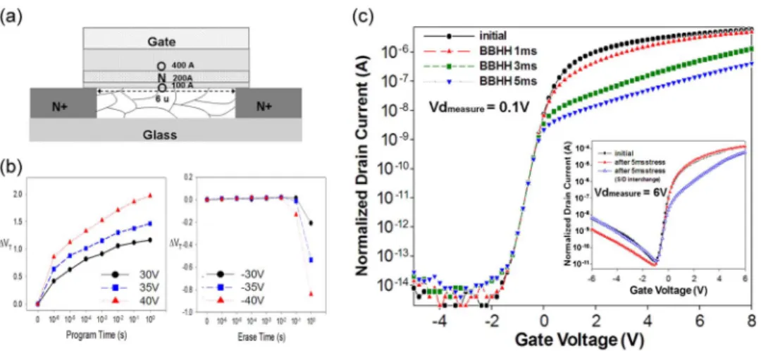
Fig. 1. (a) Schematic cross section diagram of SONOS TFTs. (b) FN program/erase characteristics with various operation bias. (c) Normalized Id–Vg
characteristics measured with Vd= 0.1 V after stress of Vgs=−15 V, Vds= 10 V for 5 ms. The inserted diagram shows saturation I–V characteristics
measured with Vgsweep from−6 ∼ 6 V and Vd= 6 V with S/D interchange and without S/D interchange before and after stress.
III. RESULT ANDDISCUSSION
Fig. 1(a) shows the schematic cross section diagram of the SONOS-TFTs and the corresponding memory characteristics utilizing FN program/erase operation are shown in Fig. 1(b). As the memory device operates inOFF-state (Vgs=−15 V and Vds= 10 V in this experiment), holes generated by the band-to-band tunneling can obtain kinetic energy in the depletion region due to the lateral field and then are injected into the nitride layer due to the vertical field [10]. Furthermore, the apparentON-state degradation after the 5-ms BBHH operation in linear region (Vd= 0.1 V) shown in Fig. 1(c) illustrates
that hot-hole injection causes interface states generation. In addition, the inset in Fig. 1(c) shows the BBHH stressed Id–Vg
characteristics in the saturation region (Vd= 6 V) with the
forward and reverse modes. For the forward mode, the S/D def-inition is the same as stress condition, but the source and drain are exchanged for the reverse mode. Clearly, the forward mode
ON-state degradation caused by the interface states is absent since the current has already spread to the bulk in the pinch-off region [11]; this is different from the reverse mode I–V characteristics. In addition, theOFF-current is suppressed in the forward mode due to the electrical field reduction resulting from the hot-hole injection near the drain side. The above results reveal that the interface state generation and hot-hole injection are asymmetric.
To clarify the asymmetric characteristics, Fig. 2 shows the initial Id–Vd characteristics and the forward/reverse modes’ Id–Vd characteristics after BBHH stress with Vgs=−15 V and Vds= 10 V for 5 ms. After stress, significant current crowding effect was observed in the smaller Vdregion for both
measurement modes because interface states induced parasitic resistance during the hot-hole injection operation near the drain side [12]. Generally, the parasitic resistance effect can be ig-nored as the device is measured in the saturation region due to the presence of the pinch-off region, as shown in the inset in Fig. 1(b). However, the Id–Vd curves show that the
for-ward mode drain current after stress starts to exceed the initial drain current as the drain bias increases to a critical value. This result suggests that the current increase can be attributed
Fig. 2. Id–Vdcharacteristics measured with Vg= 6 V and 8 V with S/D
interchange and without S/D interchange before and after stress of Vgs=
−15 V and Vds= 10 V for 5 ms.
to the trapped holes which assist electron accumulation in the SiO2/poly-Si channel interface and cause the effective channel length to decrease [13].
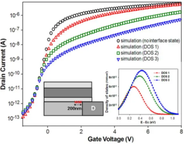
To verify that the seriousON-state degradation is caused by the interface states and analyze the trap state distribution, we utilized ISE-TCAD simulation tool to model the degradation mechanism after hot-hole injection. In this letter, the location of trap states was assumed at bottom oxide/Poly-Si interface with a 200-nm width near the drain (the diagram is shown in the inset in Fig. 3). Fig. 3 shows the simulation I–V curves with various trap density and distribution. Apparently, the degrada-tion tendency agrees closely with the experimental data shown in Fig. 1(a). In general, theON-state degradation in n-type
poly-TFTs relates to the acceptor-like states in the upper half of the energy band gap. Therefore, we adjusted the trap density and distribution, as shown in the inset of Fig. 3, and the results of the corresponding I–V curves prove that the interface states not only increased but also moved to the deep level in the upper half of band gap after continuous hot-hole injection.
Fig. 4(a) and (b) shows the relation ofON-state degradation rate between the gate stress voltage and drain stress voltage. The hole injection into the ONO layer is dependent on two fac-tors; one is the hole generation rate and the other is the energy of holes necessary to overcome the Si-SiO2barrier, which strongly
CHEN et al.: ANALYSIS OF DEGRADATION MECHANISM IN SONOS-TFT 1415
Fig. 3. Simulation Id–Vgcharacteristics with three kinds of trap states density
and distribution in the band gap. The inserted diagrams show the interface states location and the corresponding density of states distribution.
Fig. 4. Relative Ion variation, [Ion(i)− Ion(f)]/Ion(i) versus stress gate volt-age of−5, −7.5, −10, −12.5, −15 V (fixed Vds= 10 V). (b) [Ion(i)−
Ion(f)]/Ion(i) versus stress drain voltage of 0, 2.5, 5, 7.5, 10 V (fixed Vgs=
−15 V). The Ion(i) and Ion(f) are the on current, before and after stress,
measured at Vg= 10 V and Vd= 0.1 V.
depends on the vertical and lateral electrical fields, respectively. Compared with Fig. 4(a) and (b), even though the correspond-ing gate-to-drain voltage drops (Vg,stress− Vd,stress) remain
the same, the degradation rate for a fixed Vd,stressof 10 V is
much serious than that with a fixed Vg,stressof−15 V. Fig. 4(a)
shows that theON-state degradation increases with stress gate voltage and that the degradation of 40% was easily achieved after 5-ms stress with 10-V drain bias and −5-V small gate
bias. However, as shown in Fig. 4(b), the apparent degradation occurs until the drain voltage is over 9 V, even at a gate bias of
−15 V. This suggests that the degradation is more sensitive to
drain voltage because the generated holes must obtain enough energy to trigger hot-hole injection.
IV. CONCLUSION
This letter has investigated the degradation of poly-Si TFTs with SONOS structure after OFF-state stress. The apparent
ON-state degradation (more than 1 order) and the asymmetric
I–V characteristics after stress indicate the interface states
generation during the BBHH injection process. In addition, the consistent simulation result indicates that the trap states not only increased but also moved to the deep level in the upper half of band-gap after continuous hot-hole injection. Furthermore, the distinct ON-state degradation rate under different gate and drain voltages reveals that the lateral electrical field plays a more important role than the vertical electrical field during BBHH stress.
REFERENCES
[1] K. Yoneda, R. Yokoyama, and T. Yamada, “Development trends of LTPS TFT LCDs for mobile applications,” in Proc. Symp. VLSI Circuits, 2001, pp. 85–90.
[2] A. J. Walker, S. Nallamothu, E. H. Chen, M. Mahajani, S. B. Herner, M. Clark, J. M. Cleeves, S. V. Dunton, V. L. Eckert, J. Gu, S. Hu, J. Knall, M. Konevecki, C. Petti, S. Radigan, U. Raghuram, J. Vienna, and M. A. Vyvoda, “3D TFT-SONOS memory cell for ultra-high density file storage applications,” in VLSI Symp. Tech. Dig., Jun. 2003, pp. 29–30. [3] S. C. Chen, T. C. Chang, P. T. Liu, Y.-C. Wu, P.-S. Lin, B.-H. Tseng,
J.-H. Shy, S.M. Sze, C.-Y. Chang, and C.-H. Lien, “A novel nanowire channel poly-Si TFT functioning as transistor and nonvolatile SONOS memory,” IEEE Electron Device Lett., vol. 28, no. 9, pp. 809–811, Sep. 2007.
[4] Y. H. Tai, S. C. Huang, and P. T. Chen, “Degradation mechanism of poly-Si TFTs dynamically operated in OFF region,” IEEE Electron Device
Lett., vol. 30, no. 3, pp. 231–233, Mar. 2009.
[5] R. Daniel, Y. Shaham-Diamand, and Y. Roizin, “Interface states in cycled hot electron injection program/hot hole erase silicon–oxide-nitride–oxide–silicon memories,” Appl. Phys. Lett., vol. 85, no. 25, pp. 6266–6268, Jul. 2004.
[6] A. Padilla, S. Lee, D. Carlton, and T. J. K. Liu, “Enhanced endurance of dual-bit SONOS NVM cells using the GIDL read method,” in VLSI Symp.
Tech. Dig., 2008, pp. 142–143.
[7] K. R. Han, M. K. Jeong, I. Cho, and J. H. Lee, “5-bit/cell characteristics using mixed program/erase mechanism in recessed channel non-volatile memory cells,” Current Appl. Phys., vol. 10, no. 1, pp. e2–e4, Jan. 2010. [8] F. Y. Jian, T. C. Chang, and A. K. Chu, “A 2 bit nonvolatile memory device
with a transistor switch function accomplished with edge-FN tunneling operation,” Electrochem. Solid-State Lett., vol. 13, no. 5, pp. H166–H168, Mar. 2010.
[9] T. Wang, T. E. Chang, L. P. Chiang, C.-H. Wang, N.-K. Zous, and C. Huang, “Investigation of oxide charge trapping and detrapping in a MOSFET by using a GIDL current technique,” IEEE Trans. Electron
Devices, vol. 45, no. 7, pp. 1511–1517, Jul. 1998.
[10] I. Bloom, P. Pavan, and B. Eitan, “NROM—A new technology for non-volatile memory products,” Solid State Electron., vol. 46, no. 11, pp. 1757–1763, Nov. 2002.
[11] C. W. Chen, T. C. Chang, P. T. Liu, H. Y. Lu, T. M. Tsai, C. F. Weng, C. W. Hu, and T. Y. Tseng, “Electrical degradation of N-channel poly-Si TFT under AC stress,” Electrochem. Solid-State Lett., vol. 8, no. 9, pp. H69–H71, Jul. 2005.
[12] C. F. Weng, T. C. Chang, Y. H. Tai, S. T. Huang, K. T. Wu, C. W. Chen, W. C. Kuo, and T. F. Young, “Thermal analysis on the degradation of poly-silicon TFTs under AC stress,” Mater. Chem. Phys., vol. 116, no. 2/3, pp. 344–347, Aug. 2009.
[13] K. C. Moon, J. H. Lee, and M. K. Han, “The study of hot-carrier stress on poly-Si TFT employing C–V measurement,” IEEE Trans. Electron