國
立
交
通
大
學
電子工程學系 電子研究所碩士班
碩
士
論
文
適用於多核心 PlayStation 3 平台之基於多層級管線
模型的多媒體平行處理技術
Parallelizing Multimedia Applications Using Multistage
Pipeline Model on PlayStation 3
研究生: 洪正堉
指導教授: 劉志尉
適用於多核心 PlayStation 3 平台之基於多層級管線模型的多媒體
平行處理技術
Parallelizing Multimedia Applications Using Multistage Pipeline
Model on PlayStation 3
研 究 生:洪正堉
Student: Cheng-Yu Hung指導教授:劉志尉 博士
Advisor: Dr. Chih-Wei Liu國 立 交 通 大 學
電子工程學系 電子研究所碩士班
碩士論文
A Thesis
Submitted to Department of Electronics Engineering & Institute of Electronics College of Electrical and Computer Engineering
National Chiao Tung University
In partial Fulfillment of the Requirements for the Degree of Master of Science
in
Electronics Engineering November 2008
Hsinchu, Taiwan, Republic of China
適用於多核心 PlayStation 3 平台之基於多層級管線模
型的多媒體平行處理技術
研究生:洪正堉
指導教授:劉志尉 博士
國立交通大學
電子工程學系 電子研究所
摘要
未來的多媒體應用傾向採用極為複雜的演算法來處理大量資料,如高解析影像。純 軟體解決方案可以因應多樣化的多媒體標準。以處理器為主的平台可透過軟體更新以跟 上最新的多媒體標準,如此可以大大的降低研發費用並延長產品在市場的壽命。然而傳 統的單一核心處理器架構並沒有辦法提供足夠的運算能力以滿足多媒體應用的即時運 算需求。多核心處理器可以提供優異的運算能力以及彈性來處理未來高複雜度的多媒體 應用。但是相較於單核心處理器只需處理單一指令流,多核心處理器的程式撰寫非常困 難。多核心處理器程式撰寫非常花費時間而且容易出錯。多核心處理器為程式撰寫帶來 許多挑戰,包含核心間的資料傳輸、同步化以及工作負載平衡。在本論文中,我們在 PlayStation 3 多核心平台上實現可滿足高解析即時需求的 H.264 解碼。我們採用了許多 有效的策略來解決多核心處理器程式撰寫的問題。其中包括利用多層級管線模型來幫助 簡化同步問題、MFC 感知排程來減低資料傳輸問題,以及反覆程序搬移來幫助達成工 作負載平衡。經過這些方法,可節省超過 70%的傳輸處理問題,核心的使用率亦可超過 85%。我們的 H.264 解碼器效能與原始版本相比提昇了 28.13 倍,該 H.264 解碼器每秒 可以解碼超過 25 張的 1080P 高解析度影像。Parallelizing Multimedia Applications Using
Multistage Pipeline Model on PlayStation 3
Student: Cheng-Yu Hung Advisor: Dr. Chih-Wei Liu
Department of Electronics Engineering Institute of Electronics
National Chiao Tung University
ABSTRACT
Future multimedia applications tend to adopt extremely complex algorithms to process vast amount of data such as high-definition video. Software solutions are preferred, for they can rely on software patches to keep up with latest multimedia standards. The development cost can be reduced and time-in-market can be extended. However, conventional single core processors fail to meet real-time requirements. Multicore architectures provide sufficient computing power and great flexibility for tomorrow’s complex applications. However, multicore programming is far more difficult compared to conventional programming which consider only single instruction stream. Multicore programming is time-consuming and error-prone. It brings new challenges including inter-core communication, synchronization and load balancing. In this thesis, we fulfill real-time high-definition H.264 decoding on PlayStation 3 multicore platform. Several effective strategies are adopted to deal with multicore programming issues. Multistage pipeline model are utilized to simplify synchronization, MFC-aware scheduling help reduces communication overhead, while iterative task migration balance workload among processors. As a result, over 70% of communication overhead is hided; processor utilization is raised over 85%. Finally, 28.13 times performance gain is achieved compared to original JM source decoder, which can decode more than 25 1080p high-definition frame per second.
誌 謝
研究生涯轉眼即逝,兩年來受到許多人幫助及鼓勵,才能順利完成碩士學業,在此致上 最深的感激。 感謝劉志尉教授自大學專題以來的指導和照顧,老師的豐富學養及學者風範,令我受益 良多,也使我在專業知識及研究態度上更臻成熟。特別感謝李政崑教授、石維寬教授及 蔡淳仁教授,謝謝你們在百忙之中,撥冗參與論文口試,並對我的研究給予寶貴的意見, 讓此篇論文更加完備充實。 感謝陳信凱學長,學長不厭其煩地對我的研究工作步步導引,有他的指導與協助,才能 有今日的成果。學長亦師亦友,研究所生涯中與學長相處的點點滴滴,都是求學階段最 美好的回憶。 感謝實驗室學長及學弟妹們。感謝歐、阿圳、郭、國強在研究生涯中的各項指導以及協 助。感謝小黑、阿甘等學弟妹,感謝學弟妹們在研究工作上的一切幫忙。 感謝實驗室一起打拚的好兄弟:阿德、阿 VAN、HANK、電七以及李岳泰。這兩年我們 經歷了無數場挑燈夜戰的努力,也共同分享研究成果的喜悅。 感謝與我同住的室友們,感謝龜董、yij 及昭曄、謝謝你們讓我在從實驗室回到住所後, 有一份家的感覺。此外,特別感謝 Bug,在我研究遇到瓶頸時給我鼓勵與開示。你們的 存在,大大減輕了我的研究壓力以及心理負擔。 感謝所有在我研究期間給予關心與打氣的好朋友們,衷心地感謝並祝福你們。 最後,謹將本論文獻給於本月初仙逝的祖父。以及祖母、父親、母親等我最親愛的家人。 沒有你們的栽培,就沒有今日的我。希望我的表現沒有讓你們失望。 正堉 謹誌於 新竹 2008 冬C
ONTENTS
1 INTRODUCTION... 1 1.1 Multimedia Application ... 1 H.264 Standard ... 2 1.2 Multicore Architecture ... 10 1.3 Multicore Programming ... 101.4 Streaming Programming Models... 12
Parallel Stages Model... 12
Multistage Pipeline Model ... 12
1.5 Thesis Organization ... 14
2 CELL PROCESSOR... 15
2.1 Cell Architecture ... 15
PowerPC Processor Elements ... 16
Synergistic Processor Elements ... 19
Element Interconnect Bus ... 22
Inter Processor Communication ... 23
2.2 Cell Programming Environment ... 25
2.3 Related work ... 28
3 CELL PROGRAMMING USING MULTISTAGE PIPELINE MODEL... 32
3.1 Multistage Pipeline Design Flow ... 32
3.2 Multistage Task Allocation... 36
3.3 MFC-aware Scheduling ... 36 3.4 Task Migration ... 38 3.5 Pipeline Modulating ... 40 4 H.264DECODER IMPLEMENTATION... 41 4.1 Kernel Optimization... 42 PPE Profiling ... 42 Data Alignment ... 43 Motion Compensation... 44 4.2 Task Allocation... 51 4.3 Scheduling Effect ... 53 4.4 Processor Utilization ... 54 4.5 Performance Analysis... 56
5 CONCLUSIONS AND FUTURE WORK... 59
L
IST OF
F
IGURES
Figure 1-1 H.264 Decoder Block Diagram... 3
Figure 1-2 Scanning Order of Residual Blocks within a Macroblock ... 4
Figure 1-3 4x4 Luminance Prediction Modes... 5
Figure 1-4 16x16 Luminance Prediction Modes... 5
Figure 1-5 Inter Prediction of Luminance Integer-Pixel, Half-Pixel and Quarter-Pixel Positions... 7
Figure 1-6 Inter Prediction of Chrominance samples ... 7
Figure 1-7 Edge Filtering Order in a Macroblock ... 8
Figure 1-8 Dependencies in Intra Prediction Mode ... 9
Figure 1-9 Dependencies in Inter Prediction Mode ... 9
Figure 1-10 Dependencies in Deblocking Filter ... 9
Figure 1-11 Parallel Stages Model... 12
Figure 1-12 Multistage Pipeline Model ... 13
Figure 1-13 Hybrid Pipeline Parallel Model... 13
Figure 2-1 Block Diagram of Cell Broadband Engine ... 16
Figure 2-2 PPE Block Diagram ... 17
Figure 2-3 PPE Functional Units ... 17
Figure 2-4 SPE Block Diagram ... 19
Figure 2-5 SPE Functional Units ... 20
Figure 2-6 Element Interconnect Bus (EIB) ... 22
Figure 2-7 Dataflow Planning for Motion JPEG decoding on CBE processor... 29
Figure 2-8 Performance with Combinations of Optimization Techniques... 30
Figure 3-1 Strict Multistage Pipeline Model... 33
Figure 3-2 Data Flow would be Complicated after Several Migrations ... 33
Figure 3-3 Design Flow ... 34
Figure 3-4 Generalized strict multistage pipeline model ... 36
Figure 3-5 Hiding DMA Latency... 37
Figure 3-6 MFC-aware Scheduling ... 38
Figure 3-7 Filling unhided DMA latency... 39
Figure 3-8 Identifying Critical SPE for Task Migration ... 39
Figure 3-9 Task Migration for Adjusting Load Balance ... 40
Figure 3-10 Buffering between arbitrary two Processors ... 40
Figure 4-1 Modified Process Network of H.264 Decoder ... 42
Figure 4-2 Sunflower and RushHour 1080P Test Sequence ... 42
Figure 4-3 Profiling Result after granularity adjustment of H.264 Decoder... 43
Figure 4-5 Un-aligned access for arbitrary 9x9 pixels... 44
Figure 4-6 Six Registers for Eight FIRs ... 45
Figure 4-7 Byte-Shuffle Operation ... 45
Figure 4-8 9x9 Pixels Arrangement for 4x4 Luminance Submacroblock Interpolation ... 46
Figure 4-9 Inter Prediction of Luminance Sub-Pixel Cases... 46
Figure 4-10 Perform SIMD with Register A-F directly ... 47
Figure 4-11 Pack Procedure for Computing i, j, k, l, m, n, o, p ... 47
Figure 4-12 Pack Procedure for Computing c, q, s, u, d, r, t, v... 48
Figure 4-13 Pack Procedure for Computing 1, 2, i, m, 3, 4, 5, 6 ... 48
Figure 4-14 16 Cases of Luminance Interpolation... 49
Figure 4-15 16 Pixels in 2 Registers of a 4x4 Submacroblock ... 49
Figure 4-16 Unpack Procedure of a 16x16 Macroblock... 50
Figure 4-17 Computation Optimization Results of Each Kernel ... 50
Figure 4-18 Profiling Results on SPE... 51
Figure 4-19 Communication/Computation Ratio of each Kernels... 52
Figure 4-20 Task Allocation Result ... 52
Figure 4-20 MFC-aware Scheduling Result of H.264 Decoder... 53
Figure 4-21 MFC-scheduling Results... 54
Figure 4-22 Processors Utilization in Sunflower Sequence... 55
Figure 4-23 Processors Utilization in RushHour Sequence... 55
L
IST OF
T
ABLES
Table 2-1 PPE and SPE SIMD-Support Comparison ... 26 Table 4-1 Instructions Needed for Packing Procedure in 16 Cases of Luminance Interpolation... 49 Table 4-2 Performances with Different Sequences of Our Optimized H.264 Decoder ... 56
1 I
NTRODUCTION
The software-only solutions for media-rich consumer-electronics devices get more and more popular because of its low development cost and long time-in-market. Traditional computing performance gain is depending on single core development. However, single core development is diminishing nowadays because of the limitations of power consumption, memory latency, and circuit complexity. Most new processors architectures are branching into more cores rather than better cores. Multicore architectures have become the mainstream rather than the exception in computing landscape. The problem is how to exploit the parallelism and make full utilization of all cores to reach the expected performance gain with efficiency.
1.1 Multimedia Application
The data rate and compression ratio of multimedia processing are improved as the complexity of algorithm grows. In multimedia decoding applications, the high-definition (HD)
resolution is a basic requirement in many markets, such as DTV, multimedia games, and multimedia playing on monitors. The even higher performance pursued by consumers make engineers design more powerful devices while keeping the price low.
The high-end consumer electronics need to run versatile multimedia applications. For examples, audio standards are AAC, MP3, Dolby Digital (AC3), etc. And multimedia standards are M-JPEG, MPEG-1, 2, and 4, H.263, H.264, etc. Thus the implementation of multimedia coding by software is a cost-effective solution. Processor-based architectures can use software patches to keep up with new multimedia applications. However, conventional single-core processor architectures are unable to provide sufficient computing power for advanced real-time multimedia processing. Thus the parallelisms in multimedia applications should be exploited by processor-based system with high performance to meet the real-time specifications. We take H.264, the latest multimedia standard available for example and as our target. H.264 standard is introduced as following.
H.264 Standard
H.264 / MPEG-4 Part 10 is the latest video compression standard developed by the ITU-T Video Coding Experts Group (VCEG) together with the ISO/IEC Moving Picture Experts Group (MPEG). The final drafting work on the first version of the standard was completed in May 2003.
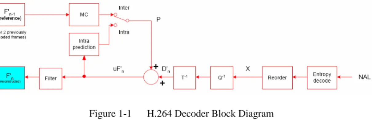
H.264/AVC provides high compression efficiency with lower bit rates. Figure 1-1 shows the H.264 decoder block diagram. The decoder receives compressed bitstream from the NAL. The data are entropy decoded and reordered to produce a set of quantized coefficients X. These are rescaled and inverse transformed to give Dn’. Using the header information decoded from the bitstream, then the decoder constructs a prediction macroblock P. P is added to Dn’ to produce uF’n which this is filtered to create the decoded macroblock F’n. The
characteristics of each block are addressed as following.
Figure 1-1 H.264 Decoder Block Diagram
z Entropy Decoding
To eliminate the syntax redundancy, the arithmetic coding is applied. The syntax above the slice layer is encoded as fixed- or variable-length codes. At the slice layer and below, H.264 standard specifies two types of entropy coding. Elements are coded using Content Adaptive Variable Length Coding (CAVLC) or Content Adaptive Binary Arithmetic Coding (CABAC) according to the entropy encoding mode.
z Quantization and Transformation
H.264/AVC uses three transforms depending on the type of residual data that is to be coded: a Hadamard transform for the 4x4 array of luminance DC coefficients in 16x16 intra-prediction macroblocks, a Hadamard transform for the 2x2 array of chrominance DC coefficients and a DCT-based transform for all other 4x4 blocks in the residual data.
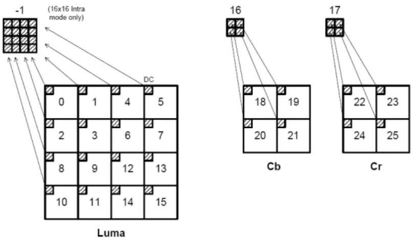
Data within a macroblock are transmitted in the order shown as Figure 1-2. If the macroblock is coded in 16x16 intra-prediction, then the block labeled ‘-1’, containing the transformed DC coefficient of each 4x4 luminance block, is transmitted first. Next, the luminance residual block 0-15 are transmitted in the order shown as Figure 1-2 (the DC coefficient in a macroblock coded in 16x16 intra-prediction mode are not sent). Block 16 and 17 containing a 2x2 array of DC coefficients from the Cb and Cr chrominance components
are sent. Finally, chrominance residual blocks 18-25 (without DC coefficients) are sent.
Figure 1-2 Scanning Order of Residual Blocks within a Macroblock
z Intra Prediction
In intra mode a prediction block is formed based on previously encoded and reconstructed blocks and is subtracted from the current block prior to encoding. The prediction block is formed for each 4x4 block or for a 16x16 macroblock for luminance samples and 8x8 macroblock for chrominance samples.
There are a total of nine optional prediction modes for each 4x4 luminance block shown as Figure 1-3. The arrows indicate the direction of prediction in each mode. For modes 3-8 the predicted samples are formed from a weighted average of the prediction samples A-M. For example, if mode 4 is selected, the top-right sample of 4x4 submacroblock is predicted by: round(B/4+C/2+D/4).
Figure 1-3 4x4 Luminance Prediction Modes
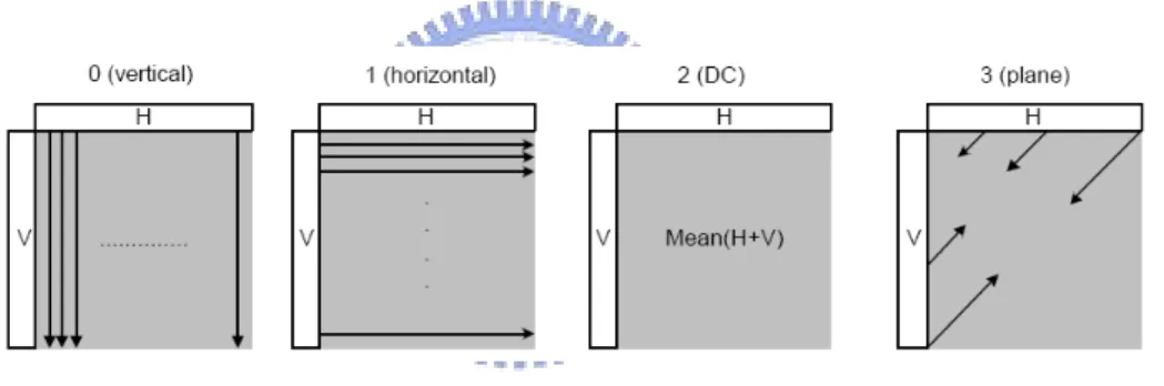
As an alternative to the 4x4 luminance prediction modes described above, the entire 16x16 luminance component of a macroblock may be predicted in one operation. Four modes are available shown as Figure 1-4.
Figure 1-4 16x16 Luminance Prediction Modes
Each 8x8 chroma component of an intra coded macroblock is predicted from previously encoded chrominance samples above and/or to the left and both chrominance components always use the same prediction mode. The four prediction modes are very similar to the 16x16 luminance prediction modes, except the numbering of the modes is different. The modes are DC (mode 0), horizontal (mode 1), vertical (mode 2) and plane (mode 3).
z Inter Prediction
Inter prediction creates a prediction model from one or more previously encoded video frames. The model is formed by shifting samples in the reference frame(s) (motion
compensated prediction). H.264 uses block-based motion compensation similar to previous standards.
H.264 supports motion compensation block sizes ranging from 16x16 to 4x4 luminance samples with many options between the two. The luminance component of each 16x16 macroblock may be split up in 4 ways including 16x16, 8x16, 16x8 and 8x8. If the 8x8 mode is chosen, each of the four 8x8 macroblock partitions within the macroblock may be split in a further 4 ways including 8x8, 4x8, 8x4 and 4x4. These partitions and sub-partitions give rise to a large number of possible combinations within each macroblock. This method of partitioning macroblocks into motion compensated sub-blocks of varying size is known as tree structured motion compensation.
A separate motion vector is required for each partition or sub-partition. Each motion vector must be coded and transmitted. The choice of each partition must be encoded in the compressed bitstream. It can cost a significant number of bits to encoding a motion vector for each partition. Since there are high correlations between motion vectors of the neighboring partitions, the motion vector can be predicted by nearby ones. Hence the motion vector prediction is generated by the motion vector of the adjacent partitions.
In order to increase the accuracy of motion compensation, H.264 supports quarter-pixel resolution for luma components and one-eight-pixel resolution for chroma components. If the prediction result of sub pixel is better than that of the integer pixel, the sub pixel will be chosen.
The half-pixel samples are obtained by applying a six tap filter with weights (1/32, -5/32, 20/32, 20/32, -5/32, 1/32). For example, a half pixel ‘b’ in Figure 1-5 is obtained from the six horizontal integer neighbors E, F, G, H, I, and J with the formulation: b = ((E- 5F+20G+20H-5I+J )/32).
Furthermore, the quarter-pixel samples can be calculated after all the half-pixel macroblock are available. They are produced by linear interpolation between two of their adjacent samples. For example, a quarter pixel ‘a’ in Figure 1-5 can be calculated by: a = (G+b)/2.
Figure 1-5 Inter Prediction of Luminance Integer-Pixel, Half-Pixel and Quarter-Pixel Positions
As shown in Figure 1-6, the chrominance samples can be calculated by linear interpolation of the neighbor pixels as following equation:
[(8-dx)(8-dy)A+dx(8-dy)B+(8-dx)dyC+dxdyD]/64
Figure 1-6 Inter Prediction of Chrominance samples
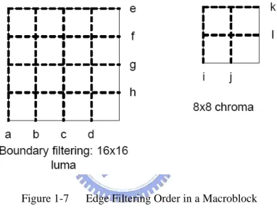
One drawbacks of the block base video compression mentioned above is the visible block boundaries. It is so called blocking effects: the lower bit rate the compression is, the more obvious the edges are. To eliminate the blocking effect, a deblocking filter is applied after the inverse transform in both encoder and decoder. As shown in Figure 1-7, it is applied to vertical or horizontal edges of 4x4 blocks in a macroblock, in the fallowing order: four vertical boundaries (a, b, c, then d) of luma, four horizontal boundaries (e, f, g, then h) of lima, and two vertical boundaries (i, j) horizontal boundaries (k, l).
Figure 1-7 Edge Filtering Order in a Macroblock
The filtering is adaptively applied according to the boundary strength and the gradient across the boundaries. The boundary strength depends on the compression mode of a macroblock, the quantization parameter, motion vector, frame or field coding decision, and pixel values. With this filter, subjective quality is significant improved. This filter also reduces the bits rate with ratio of 5%–10% compared with non-filtered video with the same objective quality.
z Data Dependencies of H.264/AVC Decoder
There are highly dependencies in H.264/AVC decoder which causing the difficulty for parallel programming. In entropy decoding, the bitstream must be decoded in order. As shown
in Figure 1-8, for a macroblock, intra prediction needs the upper macroblock and left macroblock to be decoded. A 4x4 luma submacroblock needs the upper 4x4 submacroblock, left 4x4 submacroblock and upper right 4x4 submacroblock to be decoded in advance.
Figure 1-8 Dependencies in Intra Prediction Mode
In inter prediction mode, data dependencies are within the search range of the reference frame is need for interpolation as shown in Figure 1-9.
Figure 1-9 Dependencies in Inter Prediction Mode
In deblocking filter, the four neighbor rows pixels of upper macroblock and four neighbor columns pixels of left macroblock are needed as shown in Figure 1-10.
1.2 Multicore Architecture
In recent years, processor industry has reached a new market of consumer electronics and personal computers. In order to further improve the already high performance of processor, the concept of multi-core on a chip comes out. With the improvement of semiconductor processes, it’s possible to put many processing cores onto a single processor chip. This kind of processor is called as multicore processor.
A multicore processor combines two or more independent cores into a single package composed of a single die. Cores in a multicore device may share a single coherent cache at the highest on-device cache level or may have separate caches. The processors also share the same interconnect to the rest of the system. Each "core" independently implements optimizations such as superscalar execution, pipelining, and multithreading. There are some reasons for multicore trend. First, the processor needs more effective performance per Hz, i.e., the power would become the bottleneck of processor. The utilization of more processors on a system was a common solution in the past. The multi-chip module (MCM) belongs to this category. But with the help of semiconductor technology, the integration of many circuits into a single chip is feasible.
1.3 Multicore Programming
With the advent of multicore architectures, the programmers and consumers may simply think that the performance would increase linearly with the number of cores. However, it’s always not the case as excepted. The potential problems are the level of parallelism and the communication between each core. It’s a complicated job to extract parallelism from the program and balance the workload for each core. The communication overhead in a multicore system may become the bottleneck when the communication throughput is too huge or the
frequency is too high.
Software benefits from multicore architectures where code can be executed in parallel, but traditional programming models are ill-suited to multicore architecture because they assume a single instruction stream and a monolithic memory. It is very difficult to automatically extract parallelism from a sequential program. The parallelism of task remains in the hands of programmer much of time. Thus the key point to improve the performance of a multicore processor is the task partition and communication mechanism between each core designed by the programmers. A multicore programmer requires concept and understanding of parallel programming.
The key to parallel programming is to locate exploitable concurrency in a task. The first basic step for parallelizing program is locate concurrency, then structure the algorithms to exploit concurrency, and finally tune for the performance. But achieving parallel programming with high performance by just following the basic steps described above is not easy, there are also challenges for parallel programming. First are the data dependencies. Second, there is overhead in synchronizing concurrent memory accesses or transferring data between different processor elements and memory access overhead might exceed any performance improvement. Third, partitioning work is often not obvious and can result in unequal units of work. Last, what works in one parallel environment might not work in another, due to differences in bandwidth, topology, hardware synchronization primitives, and so forth.
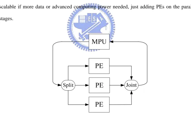
1.4 Streaming Programming Models
Parallel Stages Model
Figure 1-11 shows the parallel stages model. If the target application has low or none dependencies among kernels, the task in which there is a large amount of data that can be partitioned and acted on at the same time. But a communication mechanism is needed to design for this model for dispatching and collecting data. In the case of parallel stages model, task-to-task communication remains locally on the core if sufficient local memory size is available. Thus, this model inherently results in locality of data, so it is typically making sense to use PEs to process different portions of that data in parallel. This model is also well for scalable if more data or advanced computing power needed, just adding PEs on the parallel stages.
Figure 1-11 Parallel Stages Model
Multistage Pipeline Model
Figure 1-12 shows the Multistage Pipeline Model. If there are dependencies between kernels, a task requires sequential stages. The PEs can act as a multistage pipeline. Here, the stream of
data is sent into the first PE, which performs the first stage of the processing. The first PE then passes the data to the next PE for the next stage of processing. After the last PE has done the final stage of processing on its data, that data is returned to the MFC. As with any pipeline architecture, parallel processing occurs, with various portions of data in different stages of being processed. Multistage pipelining is typically avoided because of the difficulty of load balancing. It’s common that a certain task becomes a system bottleneck due to imbalanced loads of the processor. In addition, the multistage model increases the data-movement requirement because data must be moved for each stage of the pipeline. This model is not well for scalable because of repartitioning is needed if we want to add PE in this model.
Figure 1-12 Multistage Pipeline Model
A hybrid model also can be adopted between parallel stages model and multistage pipeline model as shown in Figure 1-13. However, this model has drawbacks of both. Design space and complexity in this model is much more raised.
MPU
PE
PE
PE
PE
Split Joint
1.5 Thesis Organization
This work proposed a programming scenario for CBE processor. The target of our method is to simplify the programming considerations on multicore with efficiency. The rest of this thesis is organized as follows.
Chapter 2 reviews the experimental platform: Cell Broadband Engine (CBE). A brief description of the architecture of Cell processor is the beginning. Two processing units called as the Power Processor Element (PPE) and the Synergistic Processor Element (SPE), the direct memory access (DMA), and the element interconnect bus (EIB) would be in the description. Then the communication mechanisms and associate application programming interface (API) are presented. Challenge of programming CBE processor is also made in this chapter.
Chapter 3 proposed a multistage pipeline model for multicore programming and a MFC-aware scheduling method for parallelizing MFC and SPU. These two features are packed into our design flow. We do computation optimization first for getting computation/communication ratio on SPE more precisely. Then analyze workload of each kernel on SPE for task allocation and MFC-aware scheduling. Apply iterative task migration for modulating workload balance among PEs. After task allocation on PEs is determined, the strict multistage pipeline model is generalized and buffer is inserted between PEs for reducing synchronization overhead.
Chapter 4 is the procedure of a case study of parallelizing H.264 decoder on PlayStation 3 multicore platform with our proposed method. Include the features of H.264 standard. A design flow including our proposed methods in chapter 3 is applied on H.264 decoder. The results of each optimization stage is showed and discussed.
2 C
ELL
P
ROCESSOR
Our target PlayStation 3 multicore platform is powered by Cell processor. Cell is a microprocessor architecture jointly developed by Sony Computer Entertainment, Toshiba, and IBM. Cell is shorthand for Cell Broadband Engine Architecture, commonly abbreviated CBEA in full. Cell combines a general-purpose Power Architecture core of modest performance with streamlined co-processing elements which greatly accelerate multimedia and vector processing applications. Chapter 2.1 introduces the Cell Broadband Engine (CBE) architecture. Chapter 2.2 gives overview of Cell Broadband Engine programming issues. Chapter 2.3 introduces our related work, including our previous work: real-time motion JPEG on PlayStation 3 and a H.264 implementation on CBE processor by Samsung Software Laboratories.
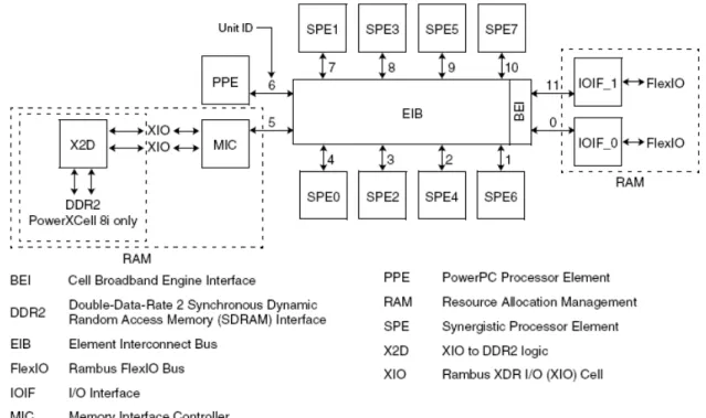
2.1 Cell Architecture
processor is a multicore processor with 9 processor elements in total and a shared coherent memory on-a-chip. The functionality of processors can be categorized into two kinds. One is the PowerPC Processor Element (PPE) and the other is the Synergistic Processor Element (SPE). There are one PPE and eight identical SPEs. All processor elements are connected to each other and to the on-chip memory and I/O controllers by the memory-coherent element interconnect bus (EIB).
Figure 2-1 Block Diagram of Cell Broadband Engine
PowerPC Processor Elements
The PowerPC Processor Element (PPE) is a general-purpose, dual-threaded, 64-bit RISC processor that conforms to the PowerPC Architecture, with the vector/SIMD multimedia extensions. The PPE consists of two main units, the PowerPC processor unit (PPU) and the PowerPC processor storage subsystem (PPSS) as shown in Figure 2-2.
Figure 2-2 PPE Block Diagram
The PPU performs instruction execution. It has a level-1 (L1) instruction cache and data cache and six execution units. It can load 32 bytes and store 16 bytes independently and memory-coherently, per processor cycle. The PPSS handles memory requests from the PPU and external requests to the PPE from SPEs or I/O devices. It has a unified level-2 (L2) instruction and data cache. The PPU and the PPSS and their functional units are shown as Figure 2-3.
PPU could further divided into the following functional units.
z Instruction Unit (IU)
The IU contains a 2-way set-associative and reload-on-error 32KB L1 instruction cache. The cache-line size is 128 bytes. The IU performs the instruction-fetch, decode, dispatch, issue, and completion portions of execution.
z Branch Unit (BRU)
The BRU performs the branch functionality.
z Fixed-Point Unit (FXU)
The FXU performs fixed-point operations, including add, multiply, divide, compare, shift, rotate, and logical instructions.
z Load and Store Unit (LSU)
The LSU contains a 4-way set-associative and write-through L1 data cache with 32 KB. The cache-line size is 128 bytes. The LSU performs all data accesses, including load and store instructions.
z Vector/Scalar Unit (VSU)
The VSU contains a floating-point unit (FPU) and a 128-bit vector/SIMD multimedia extension unit (VXU), which together execute floating-point and vector/SIMD multimedia extension instructions.
z Memory Management Unit (MMU)
The MMU contains a 64-entry segment look-aside buffer (SLB) and 1024-entry, unified, parity protected translation look-aside buffer (TLB). The MMU manages address translation for all memory accesses.
The PPSS handles all memory accesses by the PPU and memory-coherence operations from the element interconnect bus (EIB). The PPSS has a unified, 512-KB, 8-way set-associative, write-back L2 cache with error-correction code (ECC). The cache-line size for the L2 is 128 bytes as the same as L1 cache-line size. The PPSS performs data-prefetch for the PPU and bus arbitration and pacing onto the EIB. There are MMU, L1 instruction cache, and L1 data cache of PPU getting data from PPSS by a shared 32-byte load port. There are MMU and L1 data cache of PPU putting data to PPSS by a shared 16-byte store port. The interface between the PPSS and EIB supports 16-byte load and 16-byte store buses. One storage access occurs at a time, and all accesses appear to occur in program order. The interface supports resource allocation management.
Synergistic Processor Elements
The eight Synergistic Processor Elements (SPEs) execute a new single instruction, multiple data (SIMD) instruction set—the Synergistic Processor Unit Instruction Set Architecture. Each SPE is a 128-bit RISC processor specialized for data-rich, compute-intensive SIMD and scalar applications. It consists of two main units, the synergistic processor unit (SPU) and the memory flow controller (MFC), as shown in Figure 2-4.
The LS is a 256 KB, error-correcting code (ECC)-protected, single-ported, noncaching memory. It stores all instructions and data used by the SPU. It supports one access per cycle from either SPE software or DMA transfers. SPU instruction prefetches are 128 bytes per cycle. SPU data access bandwidth is 16 bytes per cycle, quadword aligned. DMA-access bandwidth is 128 bytes per cycle. DMA transfers perform a read-modify-write of LS for writes less than a quadword.
Each SPU has its own MFC. The MFC serves as the SPU’s interface, by means of the element interconnect bus (EIB), to main-storage and other processor elements and system devices. The MFC’s primary role is to interface its LS-storage domain with the mainstorage domain. It does this by means of a DMA controller that moves instructions and data between its LS and main storage. The MFC also supports storage protection on the main-storage side of its DMA transfers, synchronization between main storage and the LS, and communication functions (such as mailbox and signal-notification messaging) with the PPE and other SPEs and devices.
Figure 2-5 shows the SPE functional units. The SPU issues two instructions to its two execution pipelines respectively. The pipelines are referred to as even (pipeline 0) and odd (pipeline 1). Whether an instruction goes to the odd or even pipeline depends on the instruction type. The functional units in SPU are described as follows.
z SPU Odd Fixed-Point Unit (SFS)
The SFS executes byte shift, rotate mask, and shuffle operations on quadwords.
z SPU Load and Store Unit (SLS)
The SLS executes load and store instructions and hint for branch instructions. It also handles DMA requests to the LS.
z SPU Control Unit (SCN)
The SCN fetches and issues instructions to the two pipelines. It performs control functions such as branch instructions, arbitration of access to the LS and register file, etc.
z SPU Channel and DMA Unit (SSC)
The SSC manages communication, data transfer, and control into and out of the SPU.
z SPU Even Fixed-Point Unit (SFX)
The SFX executes arithmetic instructions, logical instructions, word SIMD shifts and rotations, floating-point comparisons, and floating-point reciprocal and reciprocal square-root estimations
z SPU Floating-Point Unit (SFP)
The SFP executes single-precision and double-precision floating point instructions, 16-bit integer multiplies and conversions, and byte operations. The 32-bit multiplies are implemented in software using 16-bit multiplies.
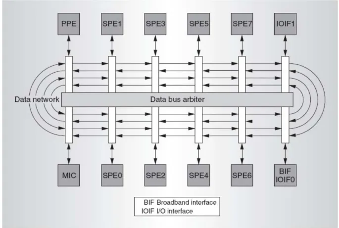
Element Interconnect Bus
Figure 2-6 shows the element interconnect bus (EIB), which is the communication path for data commands and data among the PPE, SPEs, main system memory, and external I/O. The EIB data network consists of four 16-byte-wide data rings: two running clockwise and the other two counterclockwise. Each ring allows up to three concurrent data transfers, as long as their paths don’t overlap.
Figure 2-6 Element Interconnect Bus (EIB)
To initiate a data transfer, bus elements must request data bus access. The EIB data bus arbiter processes these requests and decides which ring should handle each request. The arbiter always selects one of the two rings that travel in the direction of the shortest transfer, thus ensuring that the data won’t need to travel more than halfway around the ring to its destination. The arbiter also schedules the transfer to ensure that it won’t interfere with other
in-flight transactions. To minimize stall on reads, the arbiter gives priority to requests coming from the memory controller. It treats all others equally in round-robin fashion. Thus, certain communication patterns will be more efficient than others.
The EIB operates at half the processor-clock speed. Each EIB unit can simultaneously send and receive 16 bytes of data every bus cycle. The EIB’s maximum data bandwidth is limited by the rate at which addresses are snooped across all units in the system, which is one address per bus cycle. Each snooped address request can potentially transfer up to 128 bytes, so in a 3.2GHz Cell processor, the theoretical peak data bandwidth on the EIB is 128 bytes x1.6 GHz = 204.8 Gbytes/s.
However, the actual data bandwidth achieved on the EIB depends on several factors: the destination and source’s relative locations, the chance of a new transfer’s interfering with transfers in progress, the number of Cell chips in the system, whether data transfers are to/from memory or between local stores in the SPEs, and the data arbiter’s efficiency. EIB bandwidth would be reduced in some non-ideal cases.
Inter Processor Communication
Cell Broadband Engine (CBE) has many attributes of a shared-memory system. The PowerPC Processor Element (PPE) and all Synergistic Processor Elements (SPEs) have coherent access to main storage. But the CBE processor is not a traditional shared-memory processor. SPE only can execute programs and directly access data from and to its own local store (LS). Because of lacking directly accessing to shared memory, SPE must using three primary communication mechanisms to communicate with other elements on EIB: DMA transfers, mailbox messages, and signal notification. All these three communication mechanisms are controlled by SPE’s memory flow controller (MFC). The communication mechanisms are summarized as follow:
z DMA transfers
Used to move data and instructions between main storage and a local store(LS). An MFC supports naturally aligned DMA transfer sizes of 1, 2, 4, 8, and 16bytes and multiple of 16 bytes. For naturally aligned 1, 2, 4, and 8-byte transfers, the source and destination addresses must have the same 4 least significant bits (LSB). A single DMA command could transfer up to 16 KB between an LS and shared memory storage. The throughput of a DMA transfer when the source and destination addresses are 128-byte aligned is double as compared to that of a mis-aligned transfer within a cache line. It’s because that the mis-aligned transfer is a partial cache-line transfer, and actually there may be two bus requests for this transfer. Peak performance is achieved when the size of the transfer is a multiple of 128 bytes and both the effective address (EA) and the local store address (LSA) of the DMA transfer are 128-byte aligned. SPEs rely on asynchronous DMA transfers to hide memory latency and transfer overhead by moving data in parallel with synergistic processor unit (SPU) computation.
A MFC has only 16 entries in MFC SPU command queue. A DMA list is sequence of eight-byte list elements, stored in an SPE’s LS, each of which describes a DMA transfer and only occupy one of the SPU command queue. DMA list commands can be initiated only by SPU programs, not by other devices. A DMA list command can specify up to 2048 DMA transfers, each up to 16 KB in length. Thus, a DMA list command can transfer up to 32 MB, which is 128 times the size of the 256 KB LS, more than enough to accommodate future increases in the size of LS. The space required for the maximum-size DMA list is 16 KB. DMA list commands are used to move data between a contiguous area in an SPE’s LS and possibly noncontiguous area in the effective address space.
z Mailboxes
Supporting the sending and buffering of 32-bit messages. Each SPE can access three mailbox channels, each of which is connected to a mailbox register in the SPU’s MFC. Two one-entry mailbox channels: the SPU Write Outbound Mailbox and the SPU Write Outbound Interrupt Mailbox, which are provided for sending messages from the SPE to the PPE or other device. One four-entry mailbox channel: the SPU Read Inbound Mailbox, which is provided for sending messages from the PPE, or other SPEs or devices.
z Signal notification
Used for control communication from the PPE or other devices. SPE signal-notification channels are connected to inbound registers (into the SPE). The PPE, other SPEs, and other devices use the signal notification registers to send information, such as a buffer-completion synchronization flag, to an SPE. An SPE has two 32-bit signal-notification registers, each of which has a corresponding MMIO register that can be written with signal-notification data.
2.2 Cell Programming Environment
A source code of C/C++ program can be complied with GCC complier and executed on CBE processor with Linux environment. But an un-optimized program would be executed sequentially only on PPE without any parallelism. The CBE processor provides a foundation for many levels of parallelization. The levels of parallelization are described as follow:
z SIMD processing
Both the PowerPC Processing Element (PPE) and the Synergistic Processor Elements (SPEs) are capable of Single Instruction Multiple Data (SIMD) computation. In the PPE, these operations are supported by the 32-entry vector register file, vector/SIMD multimedia extensions to the PowerPC instruction set, and C/C++ intrinsics for the vector/SIMD multimedia extensions. In the SPEs, SIMD operations are supported by the 128-entry vector
register file, SPU instruction set, and C/C++ intrinsics.
The vector instruction sets of the PPE and the SPE are very similar. But there are still some SIMD-support differences between the PPE and SPE architectures. The differences are summarized in Table 2-1.
Table 2-1 PPE and SPE SIMD-Support Comparison
Feature PPE SPE
Number of PEs 1 8
Modes supported user and supervisor user only
Number of SIMD registers 32 (128-bit) 128 (128-bit)
Organization of register files
separate fixed-point, floating point, and SIMD
registers
unified SIMD registers
Load latency Variable (cached) fixed
Addressability 264-byte main storage 256 KB LS, 2
64
-byte main storage via DMA Memory architecture 2-level caching Software-controlled LS
SIMD instruction set
general SIMD, supported by PowerPC scalar and control
instructions
SIMD only, optimized for single-precision floating point, 16-bit fixed-point, and 32-bit fixed-point
Single-precision floating-point SIMD IEEE 754-1985 and SPE-compatible graphics-rounding mode supported extended range Double-precision
floating-point SIMD not supported IEEE 754-1985 supported Doubleword fixed-point
z Dual-issue superscalar microarchitecture
The PPE and SPEs have multiple, parallel execution units and are capable of executing two instructions per clock. Dual-issue success depends upon the instructions being issued, their address, and the state of the system during execution
z Hardware multithreading
The PPE supports two simultaneous threads of execution in hardware, so the PPE can be viewed as a two-way multiprocessor with shared dataflow. This gives PPE software the effective appearance of two independent processing units
z Multiple execution units with heterogeneous architecture and differing capabilities
Each of the nine processor elements provides independent computation and can be considered as asymmetric threads of execution. All processor elements have access to the coherent main storage for shared-memory multiprocessing. The SPE mailboxes and SPU signal notification registers support parallel-processing message-passing.
z Multiple CBE processors
Two CBE processors can be directly connected by means of the Cell Broadband Engine interface unit in a shared memory configuration. Multiple CBE processors can be loosely clustered in a distributed-memory configuration.
While these levels of parallelization are provided, there are still challenges for CBE processor programming.
z Asymmetric multicore platform
PPE is intended primary for control processing. SPEs are intended for data-rich computations allocated to them by the PPE. Task partition and allocation between PPE and
SPEs are should be carefully handled for load balancing and utilization. If the load between PPE and SPEs are imbalanced, the PPE or SPE with heaviest workload would be the bottleneck of the overall performance.
z Distributed memory architecture
Each SPE gets data from main memory through DMA transfer. DMA transfers are dynamic allocated by DMA arbiter on CBE processor. Too much DMA request at a time slice would cause the DMA transfer being the bottleneck of the overall performance. DMA commands are issued by MFC parallel with SPU computation. Hiding latency of moving data by this characteristic is an important technique in Cell programming.
z Limited scratch memory
There is only 256-KB local store (LS) for each SPE. The 256 KB LS stores both data and instructions. So the data quantity fetched into LS for computation should be carefully considered.
We adopted Sony, PlayStation 3 as our multicore platform. PlayStation 3 has 1 CBE processor which has 1 PPE and only 6 SPEs for productive. There is 256 MB memory in PlayStation 3. PlayStation 3 is a much more economical solution for construct Cell programming environment compared to Cell Blade, which has 2 CBE processor each has 1 PPE and 8 SPEs and 2GB main memory available. We installed Fedora 7 as our operating system running on PPE. GCC complier at -O3 level is adopted.
2.3 Related work
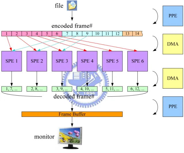
Our previous work is a frame-based data-partition on CBE processor as shown in Figure 2-7. In this work, we parallelized a motion JPEG decoder on CBE processor with 20x
improvement by using 6 SPEs. The dataflow planning starts from the input stream dividing by the PPE. The PPE allocates the encoded frames to the 6 SPEs in round-robin fashion. Each SPE is responsible for the decoding of an entire frame. The SPE returns the decoded frame and the PPE display the contents in the frame buffer. When all frames are returned, the PPE ceases the decoding process and destroys the threads.
Figure 2-7 Dataflow Planning for Motion JPEG decoding on CBE processor
There are 3 optimization techniques applied previous work. They are vectorization, parallelization, and dataflow optimization. The performance with combinations of these techniques is shown in Figure 2-8.
10 20 30 40 0 50 60 70 80 90 fps
Original Parallelization Parallelization Dataflow Opt. 100 110 52.3 5.1 4.7 46.8 108.9 10.0 Parallelization Vectorization Vectorization Parallelization Vectorization Dataflow Opt.
Figure 2-8 Performance with Combinations of Optimization Techniques
Previous work shows that data partitioning technique can achieve high utilization on SPEs for dependency-free part of a multimedia application. Unfortunately, some multimedia like H.264 standards with highly dependency is ill-suited in this manner.
In [12], D. Bader and S. Patel implement a MPEG-2 decoder on Cell Blade. They achieve 371.9 fps with 16 SPEs. They also used parallel stage, fully data partition. They offloaded whole application on SPE. Their problem is they used nearly all local store(LS). There is few space for memory optimization like double buffering.
In [13], Samsung Software Laboratories implemented H.264 decoder on CBE processor with 1 PPE and 4 SPEs. They only take PPE profiling into consideration and offload the most computation intensive functions on SPEs by intuition. They used 1/4 frame as a iteration to reduce the synchronization overhead and achieved 20 fps with 3.5x performance improvement in 1080P sequences compared to original source code on PPE. Their result shows that PPE is 95.3% busy in whole decoding process but three SPEs in charging for
Motion Compensation are only 68.1% busy. The only SPE computes Deblocking has 63.5% utilization. Their first step shows low utilization in SPEs and full loaded PPE. The bottleneck of their first implementation is the full loaded PPE. Much more functions on PPE needed to be offloaded on SPE for load balance.
In [14], Samsung Software Laboratories shows their improved second implementation. They used 1 PPE and 3 SPEs. Utilization of SPEs is raised by offloading more function of PPE to SPE. Modulate load balance between PPE and SPEs with a simple dynamic load balancing mechanism. The achieve 35 fps in 1080P test sequence and a nearly full utilization in PPE and 2 SPEs.
But in our work, we offload functions of PPE as much as possible to ease of PPE loading because our only PPE on PlayStation 3 needs to handle the OS with Linux kernel simultaneously. Our policy is offloading functions on SPEs as much as possible including computation and DMA transfer. Then hiding DMA latency by parallelizing MFC and SPU, achieve load balancing between SPEs and raise utilization of all SPEs with proposed design flow.
3 C
ELL
P
ROGRAMMING USING
M
ULTISTAGE
P
IPELINE
M
ODEL
In our thesis, a strict multistage pipeline model based design flow including task allocation, MFC-aware scheduling and iterative task migration is adopted. We provide guides for solving these three NP-complete problems in our design flow. We can get comparable performance gain by these guidelines with efficiency. Strict multistage pipeline model provides a fast way for considering task migration with efficiency. Simplify the data flow in multicore programming. MFC-scheduling is for parallelizing MFC and SPU as much as possible for hiding latency. We can hide most DMA latency with this method.
3.1 Multistage Pipeline Design Flow
In our design flow, a strict multistage pipeline model was adopted as shown in Figure 3-1. The start point and end point of the stream is the shared memory. Only the first and last processor can access shared memory. Each SPE only can access its precedence or successor’s local store (LS). If a task on a SPE is going to be migrated for loading balance. Only previous SPE and next SPE could be chosen to migrate. If performance gain is not as much as we estimated when load balance achieved. We added another available SPE at start point or end point.
Figure 3-1 Strict Multistage Pipeline Model
This strict multistage pipeline model much simplifies the design space of task migration. Considering which processor for task migrating is a complicated work. More cores adopted for parallelizing application, more choices for migration. Strict multistage pipeline model limits the choice on precedence and successor. There are always only two choices for considering regardless of the number of cores we have. The data flow between SPEs and shared memory is much simplified is strict multistage pipeline model. If we don’t restrict the model at first, the data flow between shared memory and local stores (LS) would be very complicated after several iteration of task migration as shown in Figure 3-2. In strict multistage pipeline model, data flow wouldn’t be more and more complex after several migrations.
Figure 3-3 Design Flow
Figure 3-8 briefly described our design flow. A design flow based on strict multistage pipeline model is adopted. Input of design flow is the application source code. First, we do computation optimization on application kernels with some conventional techniques including algebra simplification, SIMD, loop unrolling and software pipelining. Local optimization as better as possible is also important in multicore programming. The optimization effort in this stage influences the result of each step in our design flow afterwards.
Offloading kernels on SPE induces communication overhead. Communication overhead is comparable with computation time in some memory intensive kernel like motion compensation of H.264 decoding. How to hide DMA latency is an important issue in SPE programming. In order to hide DMA latency well, we must estimate DMA overhead as precisely as possible. Additionally, the computation time needed on PPE and on SPE might be different because their architectures are different in nature. SPE architecture is aim for high speed computation but poor for branching. PPE is opposite to SPE. So we should profile on SPE to analysis each kernel’s workload including computation and communication time.
In workload analysis on SPE, we sort communication overhead on SPE into two kinds. One is DMA issue time needed by SPU. SPU issue DMA commands to MFC costs additional cycles. Another overhead is DMA wait time. The length of DMA wait time is between MFC gets the DMA command and MFC complete the DMA command. DMA wait time needed depending on the input/output data size and data addresses in main memory is continuous or not. After computation optimization, we can get computation/communication ratio of each kernel much more precisely. So we make workload analysis on SPE for getting computation/communication ratio of each kernel which is going to be offloaded on SPEs.
After workload analysis, we allocate kernels on SPEs according to the workload analysis. We estimate the number of SPEs we needed for meet our performance constraint and the communication time we can hide roughly. Then start the allocation. We provide task allocation guides for solving this NP-complete problem with efficiency. The steps of task allocation is described in chapter 3.2.
After kernels allocated on strict multistage pipeline model, we apply MFC-aware scheduling on each SPE to hide DMA latency. MFC-aware scheduling parallelizes MFC and SPU for hiding DMA latencies. We also provide guides for this NP-complete problem. The detail of MFC-aware scheduling is described in chapter 3.3.
After MFC-aware scheduling, the latency hided in each SPE is diverse because of the computation/communication ratio in each SPE is different. As a result, MFC-aware scheduling may unbalance the workload among SPEs. So we have to do task migration after MFC-aware scheduling for modulating workload balance among all processors. An iterative task migration is adopted, which addressed in detail in chapter 3-4.
After task migration, tasks allocation is determined. If the performance is far from expected or load balance is still worse without any improvement probability. Repartitioning tasks into smaller granularities is needed. Then rerun the design flow from workload analysis.
After the result of task migration, the strict multistage pipeline model is generalized as shown in Figure 3-4. Original data flow is restricted by multistage pipeline model. In fact, not all parameters need to go through previous SPEs. Some parameter can be accessed from shared memory directly. This stage also reduces local store (LS) usage of each SPE. The remaining local store (LS) could be used for buffering. The strategy of buffering is described in chapter 3.5.
Figure 3-4 Generalized strict multistage pipeline model
3.2 Multistage Task Allocation
According to workload analysis, we can get computation/communication ratio of each kernel which is going to be allocated on SPE. There are several parameters we must estimate before allocation. We estimate the number of SPE needed for meet our required performance first to form our multistage pipeline model. Second, we assume that 60%~70% DMA latency can be hided in general scheduling result.
In our allocation procedure, each SPE has a given quota. The quota of each SPE is determined by the total workload. We fill the quota of SPEs by task allocation and allocate as balance as possible.
Then we start allocation on SPEs with strict multistage pipeline model. The allocating steps are described as follow:
z Step 1: We allocate task with the most workload with dependency first.
z Step 2: Then allocating adjacent tasks in previous task with dependency, allocating these tasks for fill quota of a SPE as much as possible.
z Back to step 1 for allocating a task with the most workload with dependency.
3.3 MFC-aware Scheduling
Once we offload a kernel on SPE. The kernel needs input/output data through DMA transfer. The procedure of a kernel executing on SPE is shown in Figure 3-5. The SPU first issues DMA command for getting input data from main memory. Then SPU wait till MFC complete the DMA transfer for computing input data. Then output data to main memory by issuing DMA command and wait for MFC completion.
We can observe that when waiting for MFC doing DMA transfer, SPU is idle. We can schedule other kernel’s computation to SPU when waiting for DMA transfer for hiding DMA latency. But getting the best scheduling result is a NP complete problem. A scenario needed for hiding DMA latency with efficiency is needed.
Figure 3-5 Hiding DMA Latency
We can schedule tasks without dependencies arbitrarily. MFC-aware scheduling can hide most of DMA latencies with highly efficiency. Take Figure 3-6 as an example. When task offload on SPE, it needs to load data for computation, then save data by DMA after execution. We take the DMA time for our MFC-aware scheduling consideration. The steps of our proposed MFC-aware scheduling are as follows
z Step 1: MFC-list optimization.
Use MFC-list command to perform scatter load/store.
z Step 2: MFC-latency hiding.
Schedule vertex pair connected by most heavy edge repeatedly. This step is aim for hiding the longest DMA latencies in a iteration.
Source vertex like load is scheduled as soon as possible.
Sink vertex like execution, save and wait are scheduled as late as possible. Overlap operation from different iterations, most DMA latencies can be hided by
this operation.
z Step 3: MFC-check minimization
Figure 3-6 MFC-aware Scheduling
3.4 Task Migration
After MFC-aware scheduling, the load balance would be worse because our task allocation is done before MFC-aware scheduling. The latency hided on each SPEs is quite different depending on each SPE’s computation/communication ratio. So task migration needed for modulating workload balance in this stage. There are two phases in task migration.
The first is trivial migration. We examine all the SPEs finding DMA latencies not hided. If there is any DMA latency not hided on a SPE, we find a proper task in adjacent SPE to fill the unhided DMA latency. This step can reduce the overall unhided DMA latency. This step is shown in Figure 3-7.
Figure 3-7 Filling unhided DMA latency
Second, we do a iterative task migration for load balancing. We identify the critical SPE by getting the utilization of each SPE. For example in Figure 3-8, SPE1 is the most critical one because of its utilization. We should migrate one of tasks on SPE1 to its adjacent for adjusting load balance as shown in Figure 3-9. The steps of iterative task migration are described as follows:
z Step 1: Identify the most critical SPE for task migration. And analysis the critical SPE which is computation dominating or communication dominating.
z Step 2: Analyze precedence and successor of the critical SPE, including their utilization and the computation/communication space for hiding. Select the one with more space for migrating task from the critical SPE.
z Step 3: Choose a task in critical SPE with proper computation/communication ratio and migrate it to the chosen SPE.
z Analyze the workload balance. Back to step 1 if the workload balance is not well.
SPE0 SPE1 SPE2 SPE3
Figure 3-9 Task Migration for Adjusting Load Balance
3.5 Pipeline Modulating
The last step of our design flow is buffering in local store. The potential problem in our multistage pipeline model is synchronization. The most serious factor is our OS handled by the PPE. PPE is the start point in our strict multistage pipeline model. Once PPE is required by OS thread, synchronization between all PPE and SPEs is influenced. Second factor is the application nature. Sometimes workload of kernel is depending on its input data or parameter. If the workload of a kernel differs from its iterations, the synchronization is influenced, too. Reducing iteration times is the most effective way for synchronization overhead reduction. Fortunately, we can add buffer between arbitrary two SPEs easily. Because the data flow in our model is simple for buffering. We can insert buffer as much as possible until the local store (LS) of a SPE is full. Moreover, we can distribute more buffers for the SPE which is more unstable in iterations. Figure 3-10 shows an example of buffering.
4 H.264
D
ECODER
I
MPLEMENTATION
In our thesis, we adopt JM H.264/AVC decoder for verifying our proposed design flow. We apply our design flow feature such as multistage pipeline model, task allocation, MFC-aware scheduling and iterative migration on official JM H.264 decoder.
Our programming environment is Sony PlayStation 3, the feature of this multicore platform is summarized as below:
z 1 CBE processor, which has 1 2-threaded PPE and 6 SPEs.
z 256MB main memory
z Fedora 7 with Linux kernel running on PPE
z SDK 3.1 with GCC complier -O3
Our H.264 decoder spec is summarized as below:
z I, P frame
z 1 reference frame
z Search range: ±16
z Prediction mode : all
z Block size: all
z 1080P, 25fps
4.1 Kernel Optimization
PPE Profiling
In our profiling, we divided motion compensation into luma MC and chroma for advanced profiling. The modified process network of H.264 decoder is shown in Figure 4-1.
Figure 4-1 Modified Process Network of H.264 Decoder
In multimedia decoding applications market, the high-definition (HD) resolution is a basic requirement. So we adopted two 1080P full HD test sequences for profiling. Sunflower and RushHour 1080P (shown as Figure 4-2) with 500 frames was analyzed.
Figure 4-2 Sunflower and RushHour 1080P Test Sequence
Profiling Result 1% 9% 14% 41% 22% 13% Intra Prediction Residue Coding VLD De-Blocking Filter Luma MC Chroma MC
Figure 4-3 Profiling Result after granularity adjustment of H.264 Decoder
We can recognize that luminance motion compensation, chrominance motion compensation and de-blocking filter are the most workload intensive part. Local optimization should be first applied on these parts. Motion compensation is the most computation intensive kernel in H.264 decoding. Therefore, we take motion compensation for example describing the way we offload a kernel on a SPE.
Data Alignment
Data in CBE processor must be aligned with a 128-bit-boundry for DMA transfers and SIMD operations. In our work, we allocate memory for pixels and vectors by using a frame as a unit and 128-bit-boundry aligned as shown in Figure 4-4. The address of pixels and vectors are continuous in x-direction.
Motion Compensation
Motion compensation is the most computation intensive part of H.264 decoder. Each 4x4 submacroblock has a separate motion vector. A 6-tap filter is used for 1/2 motion compensation. Moreover, each 4x4 submacroblock needs 9x9 pixels for compensation. It also means offloading this kernel on SPE needs high DMA bandwidth. Addresses of 9x9 pixels are non-continuous. A DMA command can only transfer continuous data in main memory. But there are only 16 entries in MFC SPU command queue.
The overhead of accessing a macroblock based pixels and vectors would be minimized in this data arrangement. But there are still extra efforts in unaligned access. For example, access arbitrary 9x9 pixels for luminance compensation needs transferring 18x9 pixels (each pixel size is 2 bytes) at least because of data un-alignment as shown in Figure 4-5.
Figure 4-5 Un-aligned access for arbitrary 9x9 pixels
To overcome the problem of limited MFC SPU command queue. We write DMA list on SPU’s LS first for issuing a large number of DMA command with only one entry in MFC SPU command queue. DMA list is used to move data between a contiguous area in an SPE’s LS and possibly noncontiguous area in the effective address space. It can specify up to 2048 DMA transfers, each up to 16KB in length.
In CBE processor, 128-bit-wide SIMD registers can contain 8 half-word integers. We can compute the 8 result of 6-tap FIR at once with 6 128-bit wide registers as shown in Figure 4-6. 9 instructions needed for computing 8 6-tap FIR results with (A+F)-(((B+E)-(C+D)<<2))x5. 4 extra instructions needed if A+F-5(B+E)+20(C+D) adopted, because 32-bit multiplication is not supported in CBE processor SIMD.
The bottleneck of SIMD optimization is the pack/unpack procedure. We can perform eight 6-tap FIRs (A-5B+20C+20D-5E+F) with six packed registers as shown in Figure 4-6.
0 1 2 3 4 5 6 7 8 10 11 12 13 14 15 16 17 18 0 1 2 3 10 11 12 13 1 2 3 4 11 12 13 14 2 3 4 5 12 13 14 15 3 4 5 6 13 14 15 16 4 5 6 7 14 15 16 17 5 6 7 8 15 16 17 18 - 5x + 20x - 5x + 20x +
Figure 4-6 Six Registers for Eight FIRs
However, the addresses of the pixels for performing FIRs are non-continuous in the memory layout. 48 instructions needed for packing 6 registers each with 8 pixels are needed in the worst case without any optimization. 8 instructions needed for unpacking the 8 pixels result. So pack/unpack procedure needed to be specified before/after SIMD operations.
In the pack/unpack procedure, the most useful instruction is byte-shuffle operation. We can arbitrarily select 1 of 32 bytes from two input quadwords for each of the 16 bytes in a output quadword according to the parameters of a third input quadword. That means we can construct one register by selecting any bytes from the two input registers as we want. Figure 4-7 shows the byte-shuffle operation.
0 1 2 3 4 5 6 7 16 17 18 19 20 21 22 23 a0 a1 a2 a3 a4 a5 a6 a7 a8 a9 a10 a11 a12 a13 a14 a15 b0 b1 b2 b3 b4 b5 b6 b7 b8 b9 b10 b11 b12 b13 b14 b15 d = spu_shuffle(a,b,c); a b c d a0 a1 a2 a3 a4 a5 a6 a7 b0 b1 b2 b3 b4 b5 b6 b7
Figure 4-7 Byte-Shuffle Operation
For each luminance 4x4 submacroblock, 9x9 pixels are needed to perform inter prediction. Our 9x9 pixels input is arranged as shown in Figure 4-8. The addresses of pixels are continuous in x-direction. So there are more instructions needed for pack if y-direction FIRs need to be performed.
Figure 4-8 9x9 Pixels Arrangement for 4x4 Luminance Submacroblock Interpolation 1 2 i j k l a b c d e f g h m n o p q r s t u v 3 4 5 6
Figure 4-9 Inter Prediction of Luminance Sub-Pixel Cases
The procedures of packing are various from the case of sub-pixel we interpolate. The cases of sub-pixels interpolation is shown in Figure 4-9. The 9x9 black squares represent 9x9 pixels needed for luminance 4x4 submacroblock interpolate.
In the example of computing sub-pixels a, b, c, d, e, f, g, h in Figure 4-9, we don’t need any pack procedure. We perform 6-tap FIRs with the register as shown in Figure 4-10 directly.
Figure 4-10 Perform SIMD with Register A-F directly
In the case of computing sub-pixels i, j, k, l, m, n, o, p in Figure 4-9, we need 7 instructions in pack procedure for SIMD operation. The pack procedure is shown in Figure 4-11.
Figure 4-11 Pack Procedure for Computing i, j, k, l, m, n, o, p
In the example of computing sub-pixels c, q, s, u, d, r, t, v in Figure 4-9, we need 10 instructions in total pack procedure for SIMD operation. The pack procedure is shown in Figure 4-12.
Figure 4-12 Pack Procedure for Computing c, q, s, u, d, r, t, v
The most complex case is computing 1, 2, i, m, 3, 4, 5, 6 in Figure 4-9, we need 20 instructions in total pack procedure. The pack procedure is shown in Figure 4-13.
Figure 4-13 Pack Procedure for Computing 1, 2, i, m, 3, 4, 5, 6
There are 16 cases in luminance 4x4 submacroblock interpolation as shown in Figure 4-14. We categorized the cases by instructions needed for pack procedure for SIMD operation.