Low Noise and High Gain RF MOSFETs on Plastic Substrates
H. L. Kao
1, Albert Chin
2,*, C. C. Huang
1, B. F. Hung
1, K. C. Chiang
1, Z. M. Lai
1, S. P. McAlister
3and
C. C. Chi
41
Nano Science Tech. Center, Dept. of Electronics Eng., Nat’l Chiao-Tung Univ., Univ. System of Taiwan,
Hsinchu, Taiwan, ROC
2
SNDL, Dept. of Electrical & Computer Eng., National University of Singapore, Singapore 119260
*
on leave from
Nano Science Tech. Center, Univ. System of Taiwan- NCTU
albert_achin@hotmail.com
3National Research Council of Canada, Ottawa, Canada
4
Dept. of Physics, National Tsing Hua Univ., Hsinchu, Taiwan, ROC
Abstract — A low minimum noise figure (NFmin) of 1.2 dB and
high associated gain of 12.8 dB at 10 GHz, were measured for 0.18 µm RF MOSFETs on plastic, made by substrate thinning (~30 µm), transfer and bonding. The performance can be further improved to 0.96 dB NFmin and 14.1 dB associated gain at 10 GHz,
under applied tensile strain, using flexible Si on plastic. A 3.5 nH inductor on plastic showed a 55% higher Q-factor with a wider frequency range, compared with that on a Si substrate.
Index Terms — RF Noise, associated gain, MOSFET, plastic. I. INTRODUCTION
The integration of RF ICs on plastic substrates is a useful technology for RF ID [1]-[2] and wireless display applications. Plastic substrates are not very lossy and are highly insulating (resistivity ~108
-109
Ω–cm) - this is ideal for RF IC integration. In contrast, VLSI-standard Si substrates have a much lower resistivity of 10 Ω-cm; this results in large RF substrate loss and poor Q-factors [3]-[12]. The performance of RF passive devices on Si can be improved by integration on high-resistivity Si substrates [9], using MEMS [10]-[12] or ion-implant translated semi-insulating (106
Ω-cm) Si technology [3]-[8]. This improvement is traded-off by the increased cost of added mask and process steps, or package costs. A challenge for integrating RF ICs on plastic is that high performance transistors are required and need to be transferred from their Si substrates, and mounted on plastic with little performance degradation. Integration with high performance RF passive devices on the plastic substrate demands that the Si substrate of the RF transistors be thinned. In this paper we report a Si substrate thinning method and successfully transfer devices onto plastic. The 30 µm thick Si RF MOSFETs on plastic showed low minimum noise figure (NFmin) of 1.2 dB
and high associated gain, 12.8 dB, at 10 GHz. This excellent RF performance on plastic is comparable with that on standard Si substrates [13]-[14]. Further improvement to 0.96 dB NFmin
and 14.1 dB associated gain at 10 GHz is obtained under applied tensile strain [15], using flexible Si (30 µm thick) on plastic. The advantage of integrating RF devices on plastic is also evident from a 3.5nH inductor: the Q-factor is improved by 55% over a wide frequency range for a device on plastic, compared with one on Si. The devices with excellent low
noise and high gain, combined with high-Q inductors are suitable for low-noise ultra-wide band (UWB) (3.1-10.6 GHz) applications.
II. EXPERIMENTAL PROCEDURE
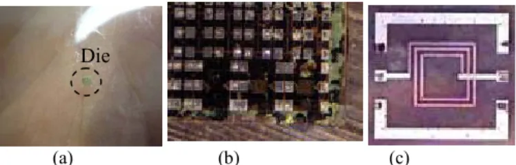
Low-cost, highly-insulating polyethylene substrates were used in this study, having a resistivity of 108-109 Ω-cm. The multiple-gate-finger (6, 16, and 32) 0.18 µm MOSFETs were designed to reduce the gate-resistance-generated thermal noise [13]-[14], which is traded-off by the increase in DC power consumption. The Si substrate of the fabricated MOSFETs was thinned down from 300 µm (6 mil) to 30 µm, using Inductive-Coupled Plasma (ICP) dry etching followed by wet chemical etching. The ICP etching provides accurate thickness-control down to 30 µm and below. The thinned devices were glued onto the plastic for DC, RF and noise testing. Fig. 1(a) shows an image of the fabricated die on transparent plastic (holding by hand- the background), where an enlarged image is shown in Fig. 1(b). The transparent substrate reveals the surface of a wooden table as the background. To use the advantages of the plastic, we fabricated a 3.5 nH inductor on it using 2 µm thick Al. For comparison a 3.5 nH inductor was also fabricated in a VLSI-standard 1-Poly-6-Metal (1P6M) foundry process. In Fig. 1(c) shows an image of an inductor on plastic, where all process temperatures were kept below 100oC.
The device characteristics were measured using HP4155C for DC, HP8510C network analyzer for S-parameter and ATN-NP5B for noise measurements.
(a) (b) (c)
Fig. 1. (a) Image of a 30 µm thick RF MOSFET die on transparent plastic. (b) Enlarged image of a die of multiple-gate 0.18 µm MOSFETs on plastic. (Background is the surface of a wooden table.) (c) Image of an inductor fabricated on plastic.
Die
III. RESULTS AND DISCUSSION
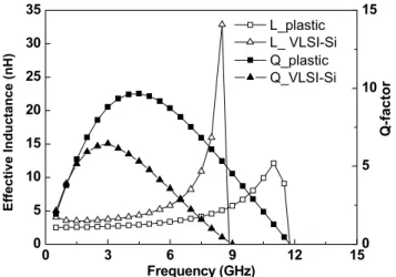
A. Q-factor of a passive inductor fabricated on plastic Figure 2 shows the measured inductance and Q-factor for a ~3.5 nH inductor on plastic. For comparison, the data for a similar 3.5 nH inductor on VLSI-standard Si is also shown. The Q-factor of the inductor is improved by 55% from 6.4 (on Si) to 10 (on plastic). The resonance frequency is also improved from 9 GHz (on Si) to 12 GHz (on plastic). These improvements are similar to our reported ion-implant translated semi-insulating Si technology [4]. However, the area cost of plastic substrates is negligible compared with that of processed 8-in Si wafers using 0.18 µm technology. The low cost and high RF performance of passive devices are important advantages for plastic electronics, in addition to the optical transparency. 0 3 6 9 12 15 0 5 10 15 20 25 30 35 0 5 10 15 L_plastic L_ VLSI-Si Q-fa ct o r Effect iv e I n d u ct an ce (n H ) Frequency (GHz) Q_plastic Q_VLSI-Si
Fig. 2. The inductance and Q-factor of a ~3.5 nH inductor on plastic and VLSI-standard 1P6M Si. The maximum temperature for fabricating the inductor on plastic was 100o
C.
B. DC characteristics of nMOSFETs on plastic
For the active transistors on plastic we first measured the DC Id-Vd characteristics. Fig. 3 shows the Id-Vd characteristic of 0.18 µm nMOSFETs with 6 gate fingers on plastic, where the Si substrate had been thinned down to 30 µm. For comparison, data for similar devices on a VLSI-standard Si substrate are also displayed. The almost identical Id-Vd
characteristics in Fig. 3, and Id-Vg characteristics (not shown),
suggest that the process of thinning down the Si substrate to 30 µm, then transferring and bonding it onto plastic, produced little degradation of the 6-finger 0.18 µm nMOSFETs. Similar observations were found for the DC Id-Vd and Id-Vg
characteristics for 16- and 32-finger devices, suggesting that they are also suitable for further RF applications and examination. 0.0 0.5 1.0 1.5 2.0 0.000 0.002 0.004 0.006 0.008 0.010 Drain Voltage (V) Dr ain Cur re n t ( A) Vg=1.8V Vg=1.2V Vg=0.6V Lg=0.18µm W=2.5µm 6 fingers
solid: on VLSI-standard Si substrate open: on plastic with 40 µm Si
Fig. 3. Measured DC Id-Vd characteristics for 6-gate-finger 0.18 µm RF MOSFETs on plastic, where the Si had been thinned down to 30 µm (open symbols). The Id-Vd of similar devices on VLSI-standard substrates, before thinning down and bonding, is included for comparison (solid symbols).
C. S-parameters and NFmin of nMOSFETs on plastic
In Figure 4(a) we show the S-parameters of a 6-gate-finger 0.18 µm RF MOSFET on plastic, where the Si substrate had been thinned down to 30 µm. For comparison, the measured S-parameters of a device on a VLSI-standard substrate are also shown. There is little S21 gain degradation as well as little change in the reverse isolation S12. The changes in both S11 and S22 are due to the increased substrate impedance when using plastic. The plastic helps reduce the substrate RF loss underneath the 6-finger MOSFETs. This result indicates that high performance RF MOSFETs can be realized on plastic.
Figure 4(b) shows a comparison of measured S-parameters for 32-gate-finger 0.18µm RF MOSFETs on a VLSI-standard substrate with those after thinning down the Si substrate to 30 µm, then transferring and mounting them onto plastic. Similar to the 6-gate-finger device case, both S11 and S22 are changed – due to the increased substrate impedance. However, the S21 gain reduces slightly - maybe due to the larger area of the device that has higher ICP plasma etching damage from the substrate-thinning step.
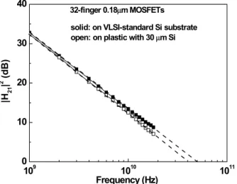
To examine the effect of the changes in S21 we compare the RF current gain of the 32-finger 0.18 µm MOSFETs before and after substrate thinning, transferal and mounting on plastic. Fig. 5 shows the RF current gain as a function of frequency. For the 32-finger 0.18 µm MOSFETs on VLSI-standard Si and plastic substrates, the |H21|2 follows the typical
-20 dB/decade slope with increasing frequency. The 10 GHz gain of the 32-finger 0.18 µm MOSFET is only slightly decreased from 13.4 dB to 12.5 dB, before and after thinning down, respectively. This high RF gain suggests that the RF MOSFETs are suitable for integration onto plastic.
0.5 1.0 2.0 5.0 -0.5j 0.5j -1.0j 1.0j -2.0j 2.0j -5.0j 5.0j S21 S12 S22 S11 6-finger 0.18 µm nMOSFET
solid: on VLSI-standard Si substrate
open: on plastic with 30 µm Si
(a) 0.5 1.0 2.0 5.0 -0.5j 0.5j -1.0j 1.0j -2.0j 2.0j -5.0j 5.0j 32-finger 0.18 µm nMOSFET
solid: on VLSI-standard Si substrate
open: on plastic with 30 µm Si
S12 Mag(S21)/4
S22 S11
(b)
Fig. 4. Comparison of the measured S-parameters of (a) 6-finger and (b) 32-finger 0.18 µm RF MOSFETs, before (solid symbols) and after substrate thinning to 30 µm, transferal and mounting on plastic (open symbols). 109 1010 1011 0 10 20 30 40 Frequency (Hz) |H21 | 2 (d B)
solid: on VLSI-standard Si substrate open: on plastic with 30 µm Si 32-finger 0.18µm MOSFETs
Fig. 5. Measured |H21|2 as a function of frequency for 0.18 µm
MOSFETs before and after substrate thinning to 30 µm, then transferal and mounting on plastic.
RF noise in front-end MOSFETs is normally the dominant noise source for the whole of an RF system. Figure 6 shows the measured NFmin and associated gain of 6-gate-finger 0.18
µm MOSFETs on plastic substrates. For comparison NFmin of
the reference devices on VLSI-standard Si substrates are also plotted. For the devices on plastic substrates, NFmin is 1.2 dB
and a high associated gain of 12.8 dB was measured at 10 GHz. Only slightly better RF performance, 0.1 dB lower NFmin
and 0.9 dB higher associated gain, were obtained for the control 0.18 µm MOSFETs at 10 GHz. These very small NFmin and associated gain differences, for the devices on
plastic and on control Si substrates, are consistent with the nearly identical S-parameters shown in Fig. 4(a). In addition the DC power consumption is only 16 mW, at the excellent low noise and high associated gain conditions.
0 5 10 15 20 0 1 2 3 0 10 20 30 40 Frequency (GHz) NF min (d B ) Associated G ain (dB)
solid: on VLSI-standard Si substrate
open: on plastic with Si substrate thinned to 30 µm 6-finger 0.18µm MOSFETs
Fig. 6. Measured NFmin and associated gain of 6-finger 0.18 µm RF MOSFETs on plastic and on VLSI-standard Si substrates.
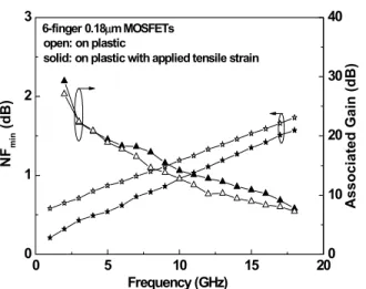
D. RF performance improvement using mechanically-applied tensile stress
An inherent merit of the 30 µm thin Si-body RF transistors on plastic is that the flexibility permits easy application of mechanical stress [15]. Fig. 7 shows the NFmin and associated
gain of 6-finger 0.18 µm MOSFETs on plastic. Under ~0.4% tensile strain, a low NFmin of 0.96 dB and high associated gain
of 14.1 dB are shown for the 0.18 µm devices on plastic at 10 GHz, which is consistent with the increased cut-off frequency (ft) from 47 to 54 GHz. These values are an improvement from
the unstrained case of 1.2 dB NFmin and 12.8 dB associated
gain, and slightly better than the control devices on a VLSI-standard Si substrate.
The excellent results for RF MOSFETs on plastic, with or without tensile strain, are comparable with the best published data [13]-[14]. These very low NFmin (0.96-1.2 dB) and high
associated gain (14.1-12.8 dB) 0.18 µm MOSFETs on plastic, are suitable for UWB applications.
0 5 10 15 20 0 1 2 3 0 10 20 30 40 Frequency (GHz) NF min (dB) Associated G ain (dB) open: on plastic
solid: on plastic with applied tensile strain 6-finger 0.18µm MOSFETs
Fig. 7. Measured NFmin and associated gain of 6-finger 0.18 µm RF MOSFETs on plastic, with or without mechanically-applied tensile strain (~0.4%).
IV.CONCLUSIONS
We have demonstrated that 0.18 µm MOSFETs, mounted on plastic after substrate thinning and die transfer, show low noise of 1.2 dB and high associated gain of 12.8 dB, measured at 10 GHz. The high performance RF transistors, combined with high-Q passive inductors, are crucial components needed to create electronics on plastic for wireless communication applications.
ACKNOWLEDGEMENT
The authors at Univ. System of Taiwan would like to thank Director S. J. King of Microelectronic Ctr, EECS Dept., UC-Berkeley for the help and G. W. Huang’s group at National Nano-Device Lab. for RF measurements.
REFERENCES
[1] R. Dekker, K. Dessein, J.-H. Fock, A. Gakis, C. Jonville, O. M. Kuijken, T. M. Michielsen, P. Mijlemans, H. Pohlmann, W. Schnitt, C. E. Timmering, and A. M. H. Tombeur, “Substrate transfer: enabling technology for RF applications,” Int.
Electron Devices Meeting (IEDM) Tech. Dig., pp. 371-374,
Dec. 2003.
[2] T. Takayama, Y. Ohno, Y. Goto, A. Machida, M. Fujita, J. Maruyama, K. Kato, J. Koyama, and S. Yamazaki, “A CPU on a plastic film substrate,” Symp. on VLSI Tech., pp. 230-231, June 2004.
[3] D. S. Yu, K. T. Chan, A. Chin, S. P. McAlister, C. Zhu, M. F. Li, and Dim-Lee Kwong, “Narrow-band band-pass filters on silicon substrates at 30 GHz,” IEEE MTT-S Int. Microwave
Symp. Dig., pp. 1467-1470, June 2004.
[4] A. Chin, K. T. Chan, H. C. Huang, C. Chen, V. Liang, J. K. Chen, S. C. Chien, S. W. Sun, D. S. Duh, W. J. Lin, C. Zhu, M.-F. Li, S. P. McAlister and D. L. Kwong, “RF passive devices on Si with excellent performance close to ideal devices designed by electro-magnetic simulation,” Int. Electron
Devices Meeting (IEDM) Tech. Dig., pp. 375-378, Dec. 2003.
[5] K. T. Chan, A. Chin, S. P. McAlister, C. Y. Chang, V. Liang, J. K. Chen, S. C. Chien, D. S. Duh, and W. J. Lin, “Low RF loss and noise of transmission lines on Si substrates using an improved ion implantation process,” IEEE MTT-S Int.
Microwave Symp. Dig., vol. 2, pp. 963-966, June 2003.
[6] K. T. Chan, A. Chin, Y. B. Chen, Y.-D. Lin, D. T. S. Duh, and W. J. Lin, “Integrated antennas on Si, proton-implanted Si and Si-on-Quartz,” Int. Electron Devices Meeting (IEDM) Tech.
Dig., pp. 903-906, Dec. 2001.
[7] K. T. Chan, A. Chin, C. M. Kwei, D. T. Shien, and W. J. Lin “Transmission line noise from standard and proton-implanted Si,” IEEE MTT-S Int. Microwave Symp. Dig., vol. 2, pp. 763-766, June 2001.
[8] Y. H. Wu, A. Chin, K. H. Shih, C. C. Wu, S. C. Pai, C. C. Chi, and C. P. Liao, “RF loss and cross talk on extremely high resistivity (10K-1MΩ-cm) Si fabricated by ion implantation,”
IEEE MTT-S Int. Microwave Symp. Dig., vol. 1, pp. 221-224,
June 2000.
[9] T. Ohguro, K. Kojima, H. S. Momose, S. Nitta, T. Fukuda, T. Enda, and Y. Toyoshima, “Improvement of high resistivity substrate for future mixed analog-digital application,” Symp.
On VLSI Tech. Dig., pp. 158-159, June 2002.
[10] P. Blondy, A.R. Brown, D. Cros, G. M. Rebeiz, "Low loss micromachined elliptic filters for millimeter wave telecommunication systems," IEEE MTT-S Int. Microwave
Symp., pp. 1181-1184, June 1998.
[11] S. Pacheco, C. T.-C. Nguyen, and L. P. B. Katehi, “Micromechanical electrostatic K-band switches,” IEEE
MTT-S Int. Microwave MTT-Symp. Dig., pp. 1569-1572, June 1998.
[12] E.-C. Park, S.-H. Baek, T.-S. Song, J.-B. Yoon, and E. Yoon, “Performance Comparison of 5GHz VCOs Integrated by CMOS Compatible High Q MEMS Inductors,” IEEE MTT-S
Int. Microwave Symp., pp. 721-724, June 2003.
[13] M.C. King, Z. M. Lai, C. H. Huang, C. F. Lee, M. W. Ma, C. M. Huang, Y. Chang and Albert Chin, “Modeling finger number dependence on RF noise to 10 GHz in 0.13 µm node MOSFETs with 80nm gate length,” IEEE RF IC Symp. Dig., pp. 171-174, June 2004.
[14] M. C. King, M. T. Yang, C. W. Kuo, Y. Chang, and A. Chin, “RF noise scaling trend of MOSFETs from 0.5 µm to 0.13 µm technology nodes,” IEEE MTT-S Int’l Microwave Symp. Dig., vol. 1, pp. 6-11, June 2004.
[15] R. E. Belford, W. Zhao, J. Potashnik, Q. Liu, and A. Seabaugh, Performance-augmented CMOS using back-end uniaxial strain,” Device Research Conference (DRC) Dig., pp. 41-42, June 2002.