A 2.4 to 5.4 GHz Low Power CMOS Reconfigurable LNA
for Multistandard Wireless Receiver
Chang-Tsung Fu, Chun-Lin Ko, and Chien-Nan Kuo
National Chiao-Tung University, Hsinchu, Taiwan
Abstract — A CMOS reconfigurable LNA is reported. Bycombination of switched inductors and varactors it performs continuous frequency tuning from 2.4 to 5.4 GHz with 500MHz 3dB-bandwidth. Switching transistor is used to provide variable gain control over a 12dB-range. The LNA supports standards including Bluetooth, WiMAX, UWB mode-1, 802.11b/g and part of 802.11a. Fabricated in 0.13um CMOS process the LNA achieves up to 25dB power gain, 2.2dB noise figure, -1dBm IIP3 while consuming less than 5mW from 1-V power supply.
Index Terms — LNA, reconfigurable, multistandard, switch inductor, dual reactive feedback.
I. INTRODUCTION
As more and more wireless applications have come into people’s life for better convenience, many communication standards are widely used currently. For roaming among different access technologies including cellular network, personal area network (PAN), wireless local area network (WLAN) and the upcoming wireless metropolitan area network (WiMAX), there rises strong motivation on using a single radio system to support bands and multi-standards to lower the hardware cost and enable wireless access anywhere and anytime. As such, the concept of so-called software-defined radio will become feasible in the future [1].
In such a multistandard RF system, one of the most critical issues is a large dynamic range to cover various needs of different standards. Consequently front-end low noise amplifier (LNA) design is of great challenge because of its noise figure and linearity requirement. While a broadband LNA faces problems including wide noise bandwidth and stringent linearity, a frequency-tuned LNA with preliminary band-selection is highly recommended. Furthermore, adjustment of gain, noise figure and linearity which provides trade-off between circuit performance and power consumption is also desirable. This demands a reconfigurable LNA to meet different specifications.
In this paper we propose a two-stage reconfigurable LNA having continuous frequency tuning from 2.4 to 5.4 GHz with 500MHz 3dB-bandwidth. It is designed to achieve broadband input matching and sufficient dynamic range at each tuned frequency while the power
consumption remains as low as possible. This LNA can be used to support multi-standards including Bluetooth, WiMAX, UWB mode-1, 802.11b/g and a part of 802.11a, as shown in Fig. 1.
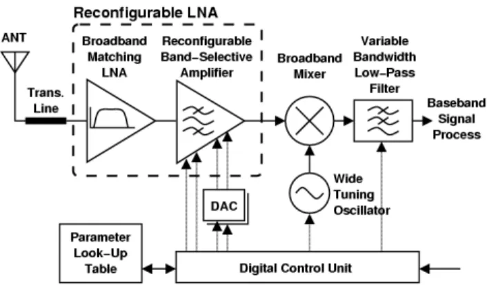
II. GENERAL CONSIDERATION ON LNADESIGN Fig. 2 is the proposed receiver front-end architecture for multistandard radio. The LNA, local oscillator and low-pass filter are controlled digitally for different specifications by the digital control unit referring to a parameter look-up table. The receiver allows the very signal of interest to pass through the receiving path, while the others turn into spurious noise to be excluded. To alleviate the issue of broadband noise, the LNA is reconfigurable to meet the required circuit performance at the tuned operating frequency over the specified 3GHz frequency range.
Functionally speaking, the reconfigurable LNA shall provide input impedance matching (S11), sufficient gain
Fig. 1. Standards included in frequency band from 2.4 to 5.4 GHz. The operation frequencies of WiMAX, from 1.7 to 5 GHz, are specified differently in different countries.
Fig. 2. Reconfigurable receiver front-end architecture.
(S21) control, good noise figure and linearity. Circuit
design complexity is further increased by the feature of frequency tuning such that a multiple-stage configuration is necessary. The dashed box in Fig. 2 shows a two-stage solution pursued in this work. Circuit property is fixed at the first stage, which provides broadband responses of input impedance matching, high voltage gain and low noise figure. This stage is set to have high voltage gain so as to achieve better system noise performance with low power consumption. Frequency tuning function is implemented at the second stage, which also provides variable gain control to enhance the dynamic range.
In general coarse tuning functions are realized using switching components controlled by open-loop digital control signals, while fine and continuous tuning using analog control signals available in current mode generated by simple low-speed digital-to-analog converters (DACs). All the digital control signals and DAC inputs refer to a look-up table which is obtained from calibration process.
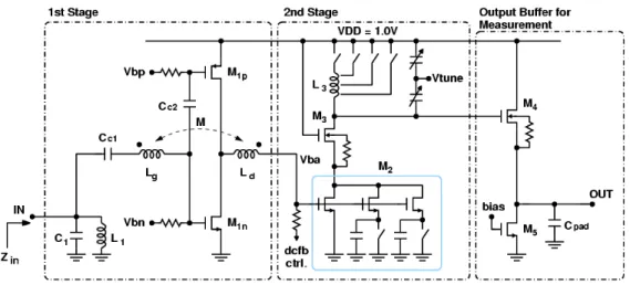
III.CIRCUIT DESIGN AND CHIP IMPLEMENTATION This LNA circuit is designed in TSMC 0.13um RF CMOS process using copper as metal material. Special processes including MiM capacitor and ultra-thick metal are used. Fig. 3 shows the schematic of the proposed reconfigurable LNA consisting of two stages. An output buffer is added for measurement purpose.
A. Broadband Input Matching
Broadband input impedance and noise matching is designed at the first stage. Frequency coverage is from 2 to 6 GHz. The design principle adopts the dual reactive feedback approach as described in [2]. By transformer and capacitor dual feedbacks, broadband performance is
implemented in a smaller die area in compare with that by the LC-ladder input source inductive degenerative configuration [3].
The DC bias at the gate nodes of M1n and M1p are
separated for low supply voltage. The voltage “Vbn” is set directly by the control unit while “Vbp” is adjusted by a DC feedback (DCFB) control loop, which samples the voltage of “Vba” and compares it with a reference voltage to adjust “Vbp” so as to make “Vba” sticking to the reference voltage. The reference voltage therefore provides certain bias control to the gate node of M2 to fine
tune the overall power gain, in additional to the coarse gain adjusting by switching transistor M2 as described next.
In this prototype “Vbn” and the reference voltage are driven externally for test purpose.
B. Variable Gain Functionality by Switching Transistor
In the second stage a CS-CG cascode topology is used and designed to be reconfigurable for variable gain and output frequency. A coarse gain control is conducted in three modes: high gain (HG), medium gain (MG) and low gain (LG) modes. For larger gain stepping the switching transistor configuration is used for M2 (Fig.3), which
consists of three parallel connected transistors in the size ratio of 1:2:4. The smallest one is always on with its source tied to ground. The source nodes of the other two transistors are connected to switches individually and AC bypassed to ground. All the three transistors are turned on in HG mode while only the smallest one is kept on in LG mode. The primary purpose using switched transistor here is to change gain without significant variation on power consumption. The switching leads to different effective total width of M2 so as to have variant gm with large
difference. The secondary purpose is to adjust linearity performance under different gain configurations. Generally in HG mode the M2 provides high power gain
Fig. 3. Proposed reconfigurable LNA.
and low noise figure while in LG mode the better linearity is provided. The additional MG mode is for better tuning continuity between HG and LG modes.
Linearity in this second stage shall be evaluated carefully. With broadband response of the first stage the second harmonic by M2 is considered critical in this LNA.
For example, the second harmonic of 2.7-GHz signal will interfere with signal of 5.4-GHz before band selective filtering. Such worst case could happen when receiving WLAN (802.11a) signal under strong interference signal of WiMAX. Fig. 4 shows the simulated gm2/gm and gm3/gm
of M2 in response to its drain current Ids, in which the gm2 is
derivative of gm and the gm3 is the second order derivative
of gm. It can be observed that at the typically chosen bias
points the second-order harmonic is suppressed around 10-dB in LG mode.
In deep submicron process the input capacitance of M2
is dominated by metal overlap capacitance so that it will not be affected much by transistor switching if all the source nodes are AC bypassed to ground (Fig.3). Hence the input matching of LNA remains steady good in different gain configurations since the change on loading capacitance of the first stage is tiny.
C. Frequency Tuning by Switching Inductor and Varactor
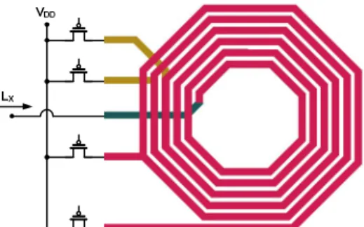
The band-pass filtering function is provided by the loading resonance tank of the second stage, which is composed by a switched inductor and a set of varactors. The switching on inductor changes the inductance and provides coarse frequency tuning while the varactor set provides fine tuning. This inductor is composed by a multi-tapped coil and PMOS switches which connect those taps to VDD individually, as shown in Fig.5. Among
the inductor switches, only one of them will be chosen turned on and all the others will be turned off to prevent dispensable eddy current flowing in the unused coil, which degrades quality factor. Considering the tuning capability of varactor the multi-tapped inductor is designed to have
40% increased inductance for each switching step so as to implement continuous frequency tuning.
As switches of the inductor the PMOS transistors have significant parasitic capacitance which make the switched inductor performs like a LC ladder structure when switches are off. When the inductor is switched for using the smallest inductance the unused part of coil will resonant with the parasitic capacitance of those opened switches and might interfere with the expected resonance tank. This limits the ratio of the largest and smallest inductance of the switched inductor. Nevertheless this parasitic resonance can be used to provide the second resonance tank which helps to keep high gain and narrow bandwidth in the highest achievable frequency region.
In this first trial we set the continuous frequency tuning range from 2.4 to 5.4 GHz. Since the quality factor of varactor changes with its capacitance the power gain of LNA will not be constant with different capacitance value. This power gain difference can also be compensated by the fine gain tuning function of the second stage.
IV.MEASUREMENT RESULTS
The micrograph of this chip is shown in Fig.6 and the circuit core size is 0.49 mm2. This chip is measured by on-wafer probing with all the DC bias voltages including Fig. 4. Simulated gm2/gm and gm3/gm of transistor M2 in
response to Ids under different gain modes. The typical bias point
of each mode is marked in the round symbol.
Fig. 5. Multi-tapped inductor with PMOS switches for switching inductance.
Fig. 6. The microphoto of the reconfigurable LNA.
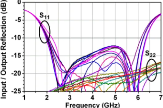
power supply are provided by wire bonding from PCB. Test chips are measured to verify circuit performance at frequencies including upper/lower frequency limits and frequencies for UWB mode-1, which are 2.40, 3.43, 3.96, 4.49 and 5.40 GHz. Both the HG mode and LG mode with the typical bias settings are tested. Fig.7 shows the measured input/output reflections (S11 and S22) in all kinds of gain/frequency configurations, which are all better than -12dB in band from 2.4 to 6.0 GHz. Fig.8 is the power gain of LNA, which is up to 25 dB in HG mode. The coarse gain difference between HG mode and LG mode is about 12 dB. Fig.9 is the measured noise figure in HG mode, showing the level from 2.2 to 3.1 dB. The
measured IIP3 in HG mode is about -1 dBm. The circuit performance is summarized listed in Table 1.
VII.CONCLUSION
A reconfigurable LNA is demonstrated in features of broadband input matching, wide frequency tuning range and variable gain. By combination of switching inductors and varactors the achieved frequency tuning ratio is larger than 2.1. By switching transistors the circuit gives 12 dB coarse gain control range while the power consumption is kept less than 5mW. The continuous frequency tuning capability makes the LNA applicable to various wireless applications applying carrier frequency within the 2.4- to 5.4-GHz frequency range.
ACKNOWLEDGEMENT
The authors wish to thank National Center for High-Performance Computing (NCHC) for software support and Chip Implementation Center (CIC) for software support and chip fabrication. The authors also thank Ansoft Corp. for technical support of EDA tools, including HFSS and Designer. This project is jointly funded by National Science Council, Taiwan, ITRI/STC JRC at NCTU and MediaTek Center at NCTU.
REFERENCES
[1] R. Bagheri et al, “Software-Defined Radio Receiver: Dream to Reality,” IEEE Comm. Magazine., vol. 44, no. 8, pp. 111-118, Aug 2006.
[2] Chang-Tsung Fu, Chien-Nan Kuo, “3~11-GHz CMOS UWB LNA using dual feedback for broadband matching,” IEEE RFIC Symp. Dig., June 2006.
[3] Chao-Shiun Wang et al, “A multi-band multi-standard RF front-end IEEE 802.16a for IEEE 802.16a and IEEE 802.11 a/b/g applications,” Proc. IEEE Int. Symp. On Circuit and Systems, pp.3974-3977, May 2005.
Fig. 9. Noise figure of the HG mode LNA of the five specified frequency configurations. Most of them are lower than 3-dB.
Table. 1 Performance summary Frequency (GHz) 2.40 3.43 3.96 4.49 5.40 S11 (dB) < -12 dB S22 (dB) < -20 dB Gain Mode HG LG HG LG HG LG HG LG HG LG S21 (dB) 22.2 10.8 23.0 11.0 24.3 12.2 22.7 11.2 25.4 13.3 NF (dB) 2.8 4.3 2.2 4.4 2.4 4.6 2.5 4.8 3.1 4.9 IIP3 (dBm) -0.5 -2.7 -0.6 -2.5 -0.0 -1.0 -2.3 -3.2 -1.0 -2.1 DC Power (mW) HG mode: 4.7 mW / LG mode: 3.6 mW (1.0V supply voltage, buffer stage excluded) Technology TSMC 0.13um RF CMOS process with UTM
Chip Size 0.49 mm2 (pads excluded) Fig. 7. Input and output reflection ratio (S11 & S22) of the LNA
under variable configurations including the specified five frequencies with HG and LG modes.
Fig. 8. Power gain of LNA under typical bias condition.