國
立
交
通
大
學
電子工程學系 電子研究所
碩
士
論
文
實現在 40 奈米製程下可操縱在低電壓的四讀四寫多
執行序暫存器叢集設計
Low VDD
MIN4R4W Multi-Thread Register File Design
and Implementation in 40nm CMOS Process
研 究 生 林弘璋
指導教授:黃 威 教授
莊景德 教授
實現在 40 奈米製程下可操縱在低電壓的四讀四寫多
執行序暫存器叢集設計
Low VDD
MIN4R4W Multi-Thread Register File Design
and Implementation in 40nm CMOS Process
研 究 生:林弘璋 Student:Hon-Jarn Lin
指導教授:黃 威 教授 Advisor:Prof. Wei Hwang
莊景德 教授 Prof.
Ching-Te Chuang
國 立 交 通 大 學
電 子 工 程 學 系 電 子 研 究 所
碩 士 論 文
A Thesis
Submitted to Department of Electronics Engineering & Institute of Electronics College of Electrical Engineering and Computer Engineering
National Chiao Tung University in partial Fulfillment of the Requirements
for the Degree of Master in
Electronics Engineering
June 2012
Hsinchu, Taiwan
I
實現在 40 奈米製程下可操縱在低電壓的四讀四寫多
執行序暫存器叢集設計
學生:林弘璋
指導教授:黃 威 教授
莊景德 教授
國立交通大學電子工程學系電子研究所
摘 要
隨著攜帶式電子產品,像是手機、筆記型電腦、影像通訊和眾多電腦商品 越來越廣泛的運用,一個低功率消耗且可提供 SoC 晶片平行處理的記憶體是非常 重要的課題。在這篇論文中分別探討了兩個主題,第一個是具有二讀二寫 8Kb 靜態隨機存取記憶體,另一個則是具有四讀四寫 2Kb 多執行序暫存器叢集設計, 兩者皆實現在 TSMC 40nm 製程上。為了達到高頻寬以及高效能,傳統單一讀寫隨 機存取記憶體無法提供夠高的效率,因此我們提出了一顆具有二讀二寫多重埠的 靜態隨機存取記憶體,此設計不僅可以解決同時列選取干擾並且可以使用於位元 交錯結構,其他設計像是相鄰共用寫入模組、CLK 閘控和電壓偵測器阻隔皆可提 供節省更多能量消耗。一個 8Kb 的測試晶片設計與實現在 TSMC 40nm 製程下,經 由電路布局後的模擬顯示,在 0.9 伏特可操作在 475 百萬赫茲。另一個設計為具 四讀四寫多執行序暫存器叢集設計,新的技術像是一周期兩次寫/讀、支援四個 序列並行、資料空位轉移和共用讀取模組。此設計提供廣泛電壓使用,可從 0.4 伏特到 1.2 伏特讓使用可以更佳有彈性。考慮低能量消耗技術像是沒有仿造讀取 動作、可降低一半讀取電路和字元線保持在高電位。藉由這些設計可大幅降低動 態能量消耗以及靜態能量消耗分別為 50%和 25%。 經由電路布局後的模擬顯示在 0.9 伏特可操作在 238 百萬赫茲。II
Low VDD
MIN4R4W Multi-Thread Register File Design
and Implementation in 40nm CMOS Process
Student: Hon-Jarn Lin Advisors: Prof. Wei Hwang
Prof. Ching-Te Chuang
Department of Electronics Engineering & Institute of Electronics
National Chiao-Tung University
ABSTRACT
There are wide-ranging usage of portable mobile device (PMD) such as cell phone, notebook and video product and many different types of computers in today markets. It is crucial important to emphasis energy efficiency, low power consumption and parallel memory design in system-on-chips (SoC) recently. In thesis, two topics will be presented. First topic is the low power 2R2W 8Kb multi-port SRAM design, second topic is the low power 4R4W 2Kb multi-thread register file design and implementation in TSMC 40nm CMOS technology. In order to gain high bandwidth and high performance, conventional single-port SRAM design is not efficiency. In this way, we proposed a new structure 2R2W multi-port bit-cell structure, this cell not only eliminate the half select distribute problem but also support bit-interleaving structure. Low power technology such as share WBL structure, CLK gating and SA power gating are included. An 8K test chip is designed and implemented in TSMC 40nm general purpose CMOS process. Post-layout simulation results demonstrate operating frequency of 475 MHz at 0.9V. Another work is 4R4W multi-thread register file design, with double pump, four threads, data slot switch control and share RBL structure technology are proposed. Wide range supply voltage operation form 0.4V to 1.2V, it supply designer has more flexibility. No dummy read operation, reducing RBL to 1/2 and RWL keep VVSS are design for low power consideration. In this work, active power reduction is more than 50% and standby power reduction is less than 25%. Post-layout simulation results demonstrate operating frequency of 238 MHz at 0.9V.
III
致 謝
可以順利完成這篇論文,有許多要感謝的人。首先,我的兩位指導老師黃威 教授和莊景德教授,感謝能給我許多寶貴的意見和優渥的研究資源,讓我在研究 時可以全力以赴不會有後顧之憂。兩位老師資深歷練,除了平時間指導我們有關 研究方面的難題,也常常教導我們人生的哲理,讓我們每每受益良多。 接著是要感謝一起打拼的學長們王道平、張銘宏、黃柏蒼、楊皓義,在研究 的路上崎嶇不平,對於一個轉組的學生更是困難重重,感謝他們不餘遺力教導和 適時的給我許多想法,讓我得以度過難關解決層層關卡。感謝 LPMD 的同學們, 因為有了你們,讓原本乏味的研究生活了增添了不少色彩,一起熬夜一起歡樂, 此外 Digital VLSI Lab 實驗室的大家,有幸大家在這一路上互相扶持跟成長, 也由衷的感謝。最後就是那些常常給我大力支持以及傾聽我苦水的工科學弟妹 們,由衷的感謝大家。最後,感謝家人對我的鼓勵與支持,也是我論文最大的推手,當我最堅實的後 盾,讓我可以一心一意的完成我的研究,在此獻上無限的感謝。
IV
Contents
Chapter 1 Introduction
1.1 Background ... 1 1.2 Challenges ... 2 1.3 Motivation ... 3 1.4 Thesis Organization ... 4Chapter 2 Previous Low-Power SRAM Designs
2.1 Introduction ... 52.2 Power Dissipation ... 6
2.2.1 Dynamic Power ... 6
2.2.2 Leakage Power ... 7
2.2.3 Short Circuit Power ... 12
2.3 SRAM Bit-cell Stability and Write-ability ... 12
2.3.1 Static Noise Margin (SNM) ... 13
2.3.2 Write Margin (WM) ... 14
2.3.3 Impact of Variation on SRAM in Low Voltage Differential 6T SRAM ... 15
2.4 Previous Read/Write Assist Peripheral Circuit ... 19
2.4.1 Keeper Tracking Circuit Assist for SRAM Design ... 19
2.4.2 Charge Pump Circuit Design ... 22
2.5 Previous Low Voltage SRAM Design ... 25
2.5.1 SRAM Bit-cell ... 25
V
2.6.1 Register File Bit-cell ... 32
2.7 Summary ... 35
Chapter 3 Low Power 2R2W Multi-Port 8Kb SRAM Design
3.1 Introduction ... 373.2 Conventional Dual-Port 8T SRAM ... 38
3.2.1 Two Kinds of Access Mode in DP-SRAM ... 38
3.2.2 Write and Read Disturb Issue in 8T DP-SRAM ... 39
3.2.3 Read/Write Conflict of Dual-port ... 40
3.3 A New 2R2W Bit-cell ... 42
3.3.1 Bit-cell Schematic and Layout View ... 42
3.3.2 Share WBL Structure ... 44
3.3.3 Bit-interleaving (8 to 1) ... 45
3.4 Write Assist Technology ... 46
3.4.1 Negative VVSS ... 46
3.4.2 Inverter Feedback Loop Cut-off ... 48
3.5 2R2W Dual-port 8Kb SRAM Design ... 49
3.5.1 2R2W Multi-port SRAM Schematic ... 49
3.5.2 Data Transmission Path ... 50
3.5.3 New Technology Adaptive in 2R2W SRAM Design ... 51
3.5.4 Test Pattern and Simulation Waveform ... 52
3.6 Post-layout Simulation ... 54
3.6.1 Performance ... 54
3.6.2 Power Consumption ... 58
VI
Chapter 4 Low-Power Register File Designs and New Bit-Cell
Structure
4.1 Introduction ... 62
4.2 Previous of Low Power Register-File Design ... 63
4.2.1 Power Reduction ... 63
4.2.2 Banked Register File Architecture ... 64
4.2.3 Tri-state Register File Design ... 67
4.3 Multi-thread Register File Design ... 68
4.3.1 Multi-thread Application Design ... 69
4.3.2 The Parity Protected Multi-thread Register File ... 70
4.3.3 Thread Switching ... 72
4.4 Timing Sharing Technology ... 74
4.4.1 Pervious Work ... 74
4.4.2 Conflict Issues ... 76
4.5 This Work ... 76
4.5.1 Bank Structure ... 76
4.5.2. Read/Write Slot Controller ... 82
4.5.3 Switch Data Circuit ... 84
4.5.4 Thread Switch Control ... 85
4.5.5 Double Pump Operation ... 87
4.6 Summary ... 89
Chapter 5 Low VDD
MINMulti-thread 4R4W Register File Design in
TSMC 40nm CMOS Process
5.1 Introduction ... 90VII
5.2 4R4W Register File Structure ... 90
5.2.1 2R2W Register File Unit Cell & Layout View ... 90
5.2.2 Share WBL Structure ... 93
5.2.3 Share RBL Structure ... 93
5.3 Register File Assist Technology ... 95
5.3.1 Negative VVSS Design ... 95
5.3.2 Single-end Write Cut-off & Y_Cut for Floating Issues Free ... 96
5.4 Implementation of Multi-thread 4R4W RF ... 97
5.4.1 4R4W Register File Floor Plane ... 97
5.4.2 Design Implementation & Test-flow of Proposed 4R4W Register File ... 99
5.5 Post-layout Simulation Result ... 102
5.5.1 Performance ... 103
5.5.2 Power Consumption ... 107
5.5.3 Iso-Area SNM Simulation and Comparison ... 110
5.6 Summary ... 112
Chapter 6 Conclusion & Future Work
6.1 Conclusions ... 114VIII
List of Figures
Fig. 1.1 Voltage scaling and energy dissipation [1.4] ... 1
Fig. 1.2 Conventional dual-port 8T SRAM bit-cell ... 2
Fig. 2.1 Circuit diagram of inverter ... 6
Fig. 2.2 Leakage current of deep-submicron transistors ... 7
Fig. 2.3 Gate leakage current paths in a NMOS transistor ... 8
Fig. 2.4 Leakage current of deep-submicron transistors ... 9
Fig. 2.5 Conventional silicon dioxide gate dielectric structure compared to a potential high-k dielectric structure ... 10
Fig. 2.6 Fin-FET structure ... 11
Fig. 2.7 Standard setup for finding Hold SNM ... 13
Fig. 2.8 Standard setup for finding Read SNM ... 14
Fig. 2.9 Write margin of a SRAM bit-cell ... 14
Fig. 2.10 The read-disturb of 6T SRAM in different process [2.17] ... 15
Fig. 2.11 The β ratio of 6T SRAM bit-cell ... 16
Fig. 2.12 6T SRAM SNM loss at low voltages [2.18] ... 17
Fig. 2.13 6T SRAM write margin [2.18] ... 18
Fig. 2.14 Read-current distribution [2.18] ... 18
Fig. 2.15 IREAD is less than Ileakage from un-accessed cells at low voltage [2.19] ... 19
Fig. 2.16 A conditional keeper with INV chain [2.20] ... 20
Fig. 2.17 A current mirror keeper [2.22] ... 20
Fig. 2.18 Cross couple keeper with INV chain (left) ... 21
IX
Fig. 2.20 Replica bias generator for RSK circuit ... 22
Fig. 2.21 The variation of the rates across different process corners ... 22
Fig. 2.22 8T SRAM cell with on-die RWL and WWL boosting [2.23] ... 23
Fig. 2.23 2SLS can Effective promotion boost ratio [2.23] ... 23
Fig. 2.24 Different boost frequency effect [2.23] ... 23
Fig. 2.25 2-step level-shifter reduce ILOAD [2.23] ... 24
Fig.2.26 Dickson charge pump circuits ... 24
Fig. 2.27 Ker proposed CP circuit and waveform with four pumping stages ... 25
Fig. 2.28 (a) The standard 2-port 8T SRAM bit-cell with non-isolated read-port [2.28] (b) An isolated read-port 7T SRAM bit-cell [2.28] ... 26
Fig. 2.29 Schematic diagram of the DCO 8T SRAM cell with dual VDD [2.29] ... 27
Fig. 2.30 DCO 8T cell shows 2x lower leakage at the same read current at 0.9V comparing to SCO 8T cell [2.29] ... 27
Fig. 2.31 Comparison of leakage components between DCO 8T cell and SCO 8T cell at 0.9V (Q = 1) [2.29] ... 27
Fig. 2.32 (a) Schematic diagram of the proposed 2-port 6T SRAM bit-cell with shared read and write assist transistors per word [2.30] ... 28
(b) The VTC and SNM obtained from butterfly curve for the standard ST, 7T and proposed 6T SRAM bit-cells [2.30] ... 28
Fig. 2.33 A 32-bit word organization of the proposed 2-port 6T SRAM bit-cell to eliminate simultaneous read/write disturbance problem [2.30] ... 29
Fig 2.34 Simultaneous R/W access issues in word-oriented array [2.30] ... 29
Fig. 2.35 Schematic of the proposed Z8T SRAM [2.31] ... 30
Fig. 2.36 Schematic of the proposed 10T SRAM [2.33] ... 31
Fig. 2.37 Schematic of the proposed 9T SRAM [2.34] ... 31
X
Fig. 2.39 Cell number on one bit-line is small [2.36] ... 33
Fig. 2.40 Two bit-cells share one bit-line [2.36] ... 33
Fig. 2.41 Cell number on one bit-line is small [2.37] ... 33
Fig. 2.42 IRF integrated memory cell circuit diagram [2.39] ... 34
Fig. 2.43 Standard 4R2W split to 2 copies of a 2R1W cell [2.41] ... 35
Fig. 3.1 Conventional 8T dual-port SRAM cell ... 38
Fig. 3.2 Different-row access mode [3.2] ... 38
Fig. 3.3 Access in the same row [3.2] ... 39
Fig. 3.4 Write operation disturbed by dummy read in the same row [3.3] ... 39
Fig. 3.5 Read operation disturbed by dummy read in the same row [3.3] ... 40
Fig. 3.6 2P-SRAM for image processing unit [3.6] ... 41
Fig. 3.7 Delay conflict waveform scheme [3.6]... 41
Fig. 3.8 2R2W multi-port SRAM bit-cell ... 42
Fig. 3.9 2R2W metal layer organization ... 43
Fig. 3.10 2R2W multi-port SRAM bit-cell layout schematic ... 43
Fig. 3.11 Two 2R2W multi-port SRAM bit-cell layout view ... 44
Fig. 3.12 One port writes with no disturb issues ... 44
Fig. 3.13 Two write the same row with no disturb issues ... 45
Fig. 3.14 8 to 1 Bit-interleaved SRAM array... 46
Fig. 3.15 Bit-interleaving select and Negative VVSS control ... 46
Fig. 3.16 Negative VVSS control circuit ... 47
Fig. 3.17 Negative level (a) Different supply voltage (b) Different corner ... 47
XI
Fig. 3.19 Conventional PMOS cut off structure ... 48
Fig. 3.20 Schematic of 8kb 2R2W SRAM Chip………..49
Fig. 3.21 Data transmission path in 2R2W SRAM chip ... 51
Fig. 3.22 2R2W 8kb SRAM array layout view ... 52
Fig. 3.23 Test pattern for 2R2W multi-port SRAM Chip ... 53
Fig. 3.24 Write test function for 2R2W multi-port SRAM chip ... 53
Fig. 3.25 Read test function for 2R2W multiport SRAM chip ... 54
Fig. 3.26 Read “0” speed with different voltage ... 54
Fig. 3.27 Write “0” speed with different voltage ... 55
Fig. 3.28 Write “1” speed with different voltage ... 55
Fig. 3.29 (a) Write conflict detect delay ... 56
Fig. 3.30 (b) Read “0” performance compare with write worst case ... 56
Fig. 3.31 Performance variation for different corner ... 57
Fig. 3.32 Write “1” speed with different voltage ... 57
Fig. 3.33 Active power consumption ... 58
Fig. 3.34 Power consumption with different voltage ... 58
Fig. 3.35 Power delay product with different voltage... 59
Fig. 3.36 2R2W multi-port SRAM pin name ... 60
Fig. 3.37 2R2W multi-port 8K SRAM test chip ... 60
Fig. 4.1 Efficiency of power gating circuits... 63
Fig. 4.2 Supply switching with ground collapse ... 64
Fig. 4.3 16-port SRAM architecture with 2-port banks and distributed crossbar ... 65
XII
Fig. 4.5 The bank-internal 1-to-8 read-port converter, ... 67
Fig. 4.6 Schematic design of novel register files ... 67
Fig. 4.7 CMT pipeline efficiency with 32 threads ... 69
Fig. 4.8 Representation of pipeline and enhancements for multithreading ... 70
Fig. 4.9 FRF double-pumped pulse clock generator circuit diagram ... 71
Fig. 4.10 SPICE simulations of both writes “0” and “1” ... 71
Fig. 4.11 Schematic of two threads switch cell ... 72
Fig. 4.12 The vector register file cell unit ... 73
Fig. 4.13 VRF cell capable of holding 2 bits and inter-bit thread decoder ... 74
Fig. 4.14 (a) Write replica circuit (b) Signal waveforms of this circuit ... 75
Fig. 4.15 Circuit cross-section of double-pumped write path ... 76
Fig. 4.16 4R4W Multi-Bank structure ... 77
Fig. 4.17 1st Data In/Out conflict detector ... 78
Fig. 4.18 1st Conflict WEN/REN detect waveform ... 79
Fig. 4.19 4R4W Multi-Bank structure………....80
Fig. 4.20 Conflict finite state machine ... 81
Fig. 4.21 S0/S1 switch control circuit ... 84
Fig. 4.22 Power7 thread decoder control circuit ... 85
Fig. 4.23 Bit cell read out architecture ... 86
Fig. 4.24 A/B port threads switch control ... 86
Fig. 4.25 Slot detected circuit ... 87
Fig. 4.27 Register files replica circuit ... 88
XIII
Fig. 5.1 The 2R2W register file unit cell ... 91
Fig. 5.2 The metal layer implement of 2R2W register file unit cell ... 92
Fig. 5.3 Layout view of 2R2W register file ... 92
Fig. 5.4 Conventional dummy read operation in half select cell ... 93
Fig. 5.5 Share RBL structure in 4R4W register file ... 94
Fig. 5.6 Share RBL structure no dummy read power consumption ... 94
Fig. 5.7 Share RBL structure in 4R4W register file ... 95
Fig. 5.8 (a) Negative level in different voltage (b) Negative level in different corner 96 Fig. 5.9 4R4W 2kb multi-thread register file floor plan ……….………97
Fig. 5.10 Test pattern and simulation waveform result ... 99
Fig. 5.11 Write post-layout simulation waveform result ... 100
Fig. 5.12 Read post-layout simulation waveform result ... 100
Fig. 5.13 Data transmission path in this 4R4W multi-threading register file ... 101
Fig. 5.14 4R4W multi-thread register file bank layout view ... 103
Fig. 5.15 Improve technologies of 4R4W register file design ... 103
Fig. 5.16 Read “0” performance for post-layout simulation ... 104
Fig. 5.17 Write “0” performance for post-layout simulation ... 104
Fig. 5.18 Write “1” performance for post-layout simulation ... 105
Fig. 5.19 (a) Address conflict detect circuit delay under wide range ... 106
(b) Delay of write worst case compare with read “0” access time. ... 106
Fig. 5.20 Power consumption with different supply voltage ... 107
Fig. 5.21 Energy consumption with different supply voltage ... 108
XIV
Fig. 5.23 Leakage power saving different voltage ... 109
Fig. 5.24 Hold static noise margin simulation ... 111
Fig. 5.25 Write trip point simulation ... 111
List of Tables
Table 3.1 Summary of the 8kb 2R2W multi-port spec ... 50Table 3.2 Characteristic of 2R2W 8kb SRAM ... 52
Table 5.1 Negative VVSS circuit function ... 96
Table 5.2 The specification of proposed ... 98
Table 5.3 Improve technology of 4R4W register file design ... 102
Table 5.4 These works compare with conventional SRAM bit-cell ... 110
1
Chapter 1
Introduction
1.1 Background
Low power design for portable device such as cell phone, wireless device and
notebook are rapidly growing in these years. A simple and effective way to reduce
energy is to scale down supply voltage. Reduction of energy consumption is desirable
in microprocessors to enable longer battery life and adequate heat dissipation. The
active power saving is quadratic and leakage power reduction is linear [1.1]–[1.3]. The
total energy consumption equation is showed in (1.1)
current short leakage dynamic total P P P P (1.1)
WherePdynamic f CVDD2,PleakageVDDIleakage,Psc VDDImean
2
Fig. 1.1 shows the SRAM Min. energy point not in the sub threshold but in near
threshold region. Operation in sub threshold region, although power reduce only
linear, delay rises significantly, and power delay product will not small anymore. This
reason make the Min. energy point is shift to neat-threshold region.
1.2 Challenges
Conventional dual-port (Fig. 1.2) or multi-port design is power hungry by accessing
many ports parallel at the same time. High frequency and multi-port read out by register
file often domain the whole chip power consumption. In order to gain high data
transmission bandwidth, this design is needed and not to be lack. Applying for portable
device, low power design is very important which can save obvious power dissipation,
and enables longer battery life.
read-word-line
R
ea
d
B
L
R
ea
d
B
Lb
write-word-line
W
rit
e
B
Lb
W
rit
e
B
L
Fig. 1.2 Conventional dual-port 8T SRAM bit-cell
Voltage scale down is not easy in conventional dual-port 8T design because read
disturb problem and read/write conflict issues will degrade cell stability. Not only cell
stability problem, write–ability is another big challenge for low voltage operation.
When supplying voltage scaling down, area of dual 8T must to enlarge cell size for
more stability. Besides, as the supply voltage is reduced, the effect of Ion/Ioff ratio is
smaller than operation in super-threshold region. Driver current normally degrades
3
In addition to CMOS technology process scaling down, there is more physic solid
state effect generated on device. Moreover, these minimum geometry transistors are
vulnerable to inter-die as well as intra-die process variations. Intra-die process variation
includes random dopant fluctuation (RDF), line edge roughness (LER). This may lead
to threshold voltage mismatch between the adjacent transistors in a memory cell giving
asymmetrical characteristics [1.5] [1.6].
1.3 Motivation
Try to do a low power and high retention SRAM cell [1.7], and no conflict
distribute problem is this work goal. Conventional dual-port already not suit for novel
technology process. A new structure must be proposed to solve distribute problem and
conflict problem. Operation under near-threshold voltage to gain the Min. energy
consumption, and this cell will apply to low power device such as wireless senor or
mobile phone. In addition to low power and high reliability, high bandwidth support
is another primary circuit concern. Multi-thread and multi-bank structure design may
include in this work for performance improve.
Except scaling down the supply voltage, peripheral circuit will use low power
design such as power gating, CLK gating, and DVS technology may added for active
or standby power reduction [1.8]. Boost or Negative circuit can improve write-ability
when operation under low voltage. Previous work like cut off feedback in single-end
design also can gain more write ability. In this design, power reduction is more
important than high speed operation.
For more robust consideration, bit-interleaving structure can eliminate soft error
rate damage the SRAM bit-cell. Leakage problem in BL can’t be ignored in low
voltage operation region. If leakage current is too over reliability, read operation will
4
1.4 Thesis Organization
Following is the main contents of this thesis. In Chap 2 we will discuss the recent
work about low power SRAM design. A conventional 6T SRAM basic operation and
stability are introduced at first. After that low power SRAM assists circuit design,
multi-port SRAM and register file design are discuss step by step. Chapter 3 shows
conventional dual-port operation conflict problem and read disturb issues. A new
2R2W multi-port SRAM structure is proposed. Share write bitline and X and Y cut
control line can do bit-interleaving structure and no need any others periphery circuit.
In Chap. 4, register file with multi–thread and double pump technology introduced at
beginning. New technology “Data Slot Switch” and conflict detect circuit can help no
disturb issue. In Chap 5, a new share read bitline is proposed and reduce dummy read
of bit-interleaving structure. Active power saves by share RBL and leakage power
reduces by keep RWL high in standby mode. In the end, Chapter 6 finally concludes
5
Chapter 2
Previous Low-Power SRAM Designs
2.1 Introduction
In recent microprocessors, the capacity of on-chip memory is rapidly increasing
to improve overall performance. According to ITRS roadmap in 2002 [2.1] [2.2],
memory chip will occupy 90% of chip area in 2013. In such a memory rich chip, the
leakage current of an SRAM, which comprises the vast majority of on-chip transistors,
dominates the standby current because leakage power is proportional to the number of
transistors. Thus, it becomes important to focus on SRAM standby leakage current
reduction for ultra-low power application.
Low power, minimum transistor count and fast access SRAM is essential for
embedded multimedia and communication applications realized using system on a
chip technology. Hence, simultaneous or parallel read/write (R/W) access multi-port
SRAM bit cells are widely employed in such embedded systems. Multi-port has many
advantages like high performance and high bandwidth, but it also consumers more
percentages of power and area.
This chapter begins with the analysis of power dissipation of SRAM circuit and
technique for leakage reduction will be shown in section 2.2. In section 2.3, stability
issues of SRAM cell, including hold stability, read stability, and write ability will be
defined and the impact of variation on SRAM in low voltage will be presented. In
section 2.4, 2.5 and 2.6, Conventional dual port SRAM and Multi-port SRAM cell are
showed. Finally, In 2.7 the previous Multi-port register file cell design and peripheral
6
2.2 Power Dissipation
This chapter begins with an analysis of power dissipation of CMOS circuit and
circuit technique for power dissipation. Power dissipation combines with dynamic
power (Pdynamic), leakage power (Pleakage), and short circuit power (Pshort-circuit). Power
could be expressed as, where Pdynamic = α CLVDD2f, Pleakage = VDDIleakage, and
Pshort-circuit=ImeanVDD
Ptotal = Pdynamic+ Pleakage+ Pshort−circuit (2.1)
2.2.1 Dynamic Power
Fig. 2.1 show a CMOS inverter, the average dynamic power dissipation can be
obtained by summarizing the average dynamic power of N/P MOS. The cause of
dynamic power is logic transition of CMOS circuits which charges or discharges its
load capacitance and parasitic capacitance (CL). As can be seen in (2.1), the dynamic
power dissipation is direct proportion to switching activity factor (α), capacitance load
(CL), squire of supply voltage (VDD2), and operating frequency (f).
VDD
GND
V
INV
OUTiN
iP
C
L7
2.2.2 Leakage Power
Fig. 2.2 Leakage current of deep-submicron transistors
In advanced CMOS technologies, embedded SRAM leakage current becomes
dominant compared to the dynamic current. The majority of SRAM macro leakage
current is from its bit cell array [2.3]. Leakage current is composed of reverse-biased
junction leakage current (IREV), gate induced drain leakage (IGIDL), gate
direct-tunneling leakage (IG), and sub-threshold leakage (ISUB) in a CMOS transistor
[2.4] [2.5].
Fig. 2.2 shows reverse-biased junction leakage, sub-threshold leakage, gate
direct-tunneling leakage, injection of hot carriers from substrate to gate oxide, gate
induced drain leakage, and punch through leakage in the deep scaling transistor.
Junction Leakage
In Fig. 2.3, leakage in reverse biased transistors and diodes includes the effects of
carrier generation, related to residual damage density and location relative to the
junction boundary, as well as structure and bias dependent effects of gate oxide
leakage, band-to-band tunneling at the drain junction and thermionic emission from
metal contacts. All of these effects depend on process conditions, through dependence
on dopant activation and profile shape, junction location and local electric fields. Subthreshold Punchthrough GIDL Reverse bias diode Gate Oxide Tunneling Gate Source Drain n+ n+ Well P
8
Fig. 2.3 Gate leakage current paths in a NMOS transistor
In the steady-state ON region both the gate and drain of the device are held at high
with the source being grounded. In this state a well-formed channel exists and three
separate components of the gate tunneling current Igs, Igcs and Igcd are active. The
component from gate to drain overlap (Igd) is absent due to the almost zero electric
field in that region of the oxide. The overall current flow is from gate to source and
channel, opposite to the flow in the OFF state. In the steady-state OFF region both
gate and source are at ground while the drain is at high (VDD) voltage. Since no
channel is formed in this condition, the only active component is Igd [2.6].
Gate-induced drain leakage (GIDL):
As the electric field in and around the gated p-n junction is increased by the
applied gate voltage, all the high-field effects, such as avalanche multiplication and
band-to-band tunneling, can increase very dramatically (Fig. 2.4). Thus, the leakage
current of a reverse-biased gated diode can increase dramatically when the gate voltage
9
Fig. 2.4 Leakage current of deep-submicron transistors
Sub threshold Leakage
When gate voltage is below the threshold voltage, sub-threshold leakage or weak
inversion current occurs between source and drain. For example, an off state inverter,
although the Vgs of the NMOS is 0V, there is a light current (leakage) flowing from the
drain to source due to the voltage VDD across Vds [2.7].
Sub-threshold behavior can be modeled physically as show in the following [2.8]
𝐼𝑑𝑠 = 𝜇𝑊𝐿 (𝑘𝑇𝑞)2𝐶𝑠𝑡ℎ𝑒𝑉𝑔−𝑉𝑇+𝜂𝑉𝑑𝑠𝑚𝑘𝑇 𝑞⁄ (1 − 𝑒−𝑘𝑇 𝑞𝑉𝑑𝑠⁄ ) , 𝑚 = 1 +𝐶𝑠𝑡ℎ
𝐶𝑜𝑥 (2.2)
Where W and L denote the transistor width and length, μ denotes the carrier mobility,
Csth = Cdep = Cit denotes the summation of the depletion region capacitance and the
interface trap capacitance both per unit area of the MOS gate, η is the drain induce
barrier lowering (DIBL) coefficient, and Cox denote the gate input capacitance per unit
area of the MOS gate.
Sub-threshold leakage increases exponentially with the reduction of the threshold
voltage and DIBL would lower threshold make leakage even worse. On the other hand,
sub-threshold can be drop with increasing the threshold voltage. In low power
technology we can use high Vth technology transistor to reduce sub-threshold leakage in
10
High-K Metal Gate
In order to reduce gate leakage, a new material is used for replace the conventional
SiO2. Silicon dioxide has been used as a gate oxide material for decades. As transistors
have decreased in size, the thickness of the silicon dioxide gate dielectric has steadily
decreased to increase the gate capacitance and thereby drive current, raising device
performance. As the thickness scales below 2 nm, leakage currents due to tunneling
increase drastically, leading to high power consumption and reduced device reliability
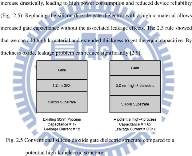
(Fig. 2.5). Replacing the silicon dioxide gate dielectric with a high-κ material allows
increased gate capacitance without the associated leakage effects. The 2.3 rule showed
that we can add high k material and extended thickness to get the equal capacitive. By
thickness oxide, leakage problem can reduce significantly [2.9].
Fig. 2.5 Conventional silicon dioxide gate dielectric structure compared to a
potential high-k dielectric structure
𝐶 =𝑘∈0𝐴
𝑡 (2.3)
A is the capacitor area
κ is the relative dielectric constant of the material (3.9 for silicon dioxide )
ε0 is the permittivity of free space
11
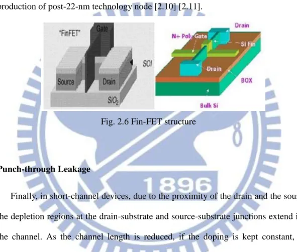
Fin FET Structure
Fig.2.6 shows Fin FET device has especially faster switching times and higher
current density. Not like conventional MOS structure, a new better gate control device
is developed by IBM. Vertical gate has more area cover the channel, so better control
ability is approach. Due to its superior gate control, electrostatic integrity, and
variability, Fin FET has demonstrated satisfactory scalability and feasibility for mass
production of post-22-nm technology node [2.10] [2.11].
Fig. 2.6 Fin-FET structure
Punch-through Leakage
Finally, in short-channel devices, due to the proximity of the drain and the source,
the depletion regions at the drain-substrate and source-substrate junctions extend into
the channel. As the channel length is reduced, if the doping is kept constant, the
separation between the depletion region boundaries decreases. An increase in the
reverse bias across the junctions (with increase in VDS) also pushes the junctions nearer
to each other. As the combination of channel length and reverse bias leads to the
merging of the depletion regions, punch through leakage occurs.
Punch through will bring a high current, and make the device short down. Hot and
12
2.2.3 Short Circuit Power
When CMOS switch frequently, a path from vdd to gnd will short together. This dc
path makes external power consumption. Short circuit power can be expressed as rule
(2.4). Imean is the mean value of the short circuit current [2.12].
On the circuit-level, there have been a number of articles describing the short
circuit power. From the short circuit power articles by Veendrick [2.13], and
Hedenstierna and Jeppson [2.14], these power dissipation rules are showed below.
P
short-circuit=I
meanx V
DD (2.4) f V V Pshortcircuit DD t 3 ) 2 ( 12 (2.5)P: The device transistor conductance τ: The ramp time
β: The gain factor of a transistor, f: The operating frequency
2.3 SRAM Bit-cell Stability and Write-ability
When CMOS technology process is scaling down, process variation is become
more and more important. PVT variation is the major effect on cell stability, such as
global variation and local variation. Therefore, how to use the simulation information
to accurate the true threshold is very important. The worst cast must be consider and
usually use Monte Carlo simulation to detect it. The following of this section will
13
2.3.1 Static Noise Margin (SNM)
The best common way to measure the stability of cross-coupled inverters is the
static noise margin (SNM). Hold static noise margin is defined as the maximum value
of static DC voltage noise which can be tolerated by the SRAM bit-cell without flipping
the storage node when word-line turns off. Fig. 2.7 shows the normal test Hold SNM
simulation in 6T SRAM cell. Give a two noise in the Q and Qb then find max voltage
noise can maintain the storage data of the SRAM. In this case, WL is zero and two BL
keep high [2.15].
Fig. 2.8 shows the standard setup for modeling Read SNM. Compare with HSNM
mode, in this case WL is turn and simulation read operation. The node “0” will raise a
little voltage because of the voltage dividing effect between the pass transistor and
pull-down transistor. Once the disturb voltage rise near to the trip point of the inverter,
data will be flipped. The curve is small than HSNM because read distribute issues and
it reduce node stability significantly. Fig. 2.7 and Fig. 2.8 also show the example of
butterfly curves during hold and read, revealing the degradation in SNM during read.
0 VDD 0 VDD VR (V ) VL (V) WL=0 BL=VDD BLb=VDD VL VR VN VN
14 0 VDD 0 VDD VR (V ) VL (V) WL=VDD BL=VDD BLb=VDD VL VR VN VN
Fig. 2.8 Standard setup for finding Read SNM
2.3.2 Write Margin (WM)
There are many way to measure the write ability of SRAM bit-cell, the simple one is find the write trip point (WTP). Write margin is defined as𝑉𝐷𝐷− 𝑀𝐼𝑁[𝑉(𝑊𝑊𝐿)]. 𝑀𝐼𝑁[𝑉(𝑊𝑊𝐿)] is the minimum write-word-line voltage required for flipping the bit-cell. In this write margin test mode, sweep WL voltage from VDD to Zero. The
higher write margin, the easier the data is written into bit-cell. Fig. 2.9 shows a
corresponding example of finding write margin. The write margin is defined as the VDD
- VWL value at the point when VR and VL flip. The write margin value and variation is a function of the cell design, SRAM array size and process variation. A cell is considered
not writeable if the worst-case write margin becomes lower than the ground potential.
VWL(V) In te rn al n od e vo lta ge VL VR 0 VDD VW L( V) VDD 0 Write trip pointer WL=VWL BL=0 BLb=VDD VL VR
15
2.3.3 Impact of Variation on SRAM in Low Voltage
Differential 6T SRAM
6T bit-cell is not applied for process scaling down, and also not suitable in
low-voltage operation. If 6T cell want to operate under novel technology, area of
N/PMOS has to enlarge to gain more W/R ability. Process problem to 6T cell is very
sensitive, such as random dopant fluctuation (RDF) and line edge roughness (LER).
This may result in the threshold voltage mismatch between the adjacent transistors in
memory cell [2.16] [2.17].
Half select disturbs Failure
In Nano-device scaling down, threshold voltage variation is become larger. By
process variation NMOS Vt is not a constant value anymore, if disturb voltage is
larger than bit-cell trip voltage, the data will flip and error happened. Conventional 6T
with bit-interleaving structure will have half select problem. Fig. 2.10 shows the half
select disturbs failure and waveform, if pull-down NMOS Vt is too high, and access
NMOS Vt is low. Current is stack on the Qb, a probability data will flip by this
current path.
16
Read/Write conflict issues
In this configuration, both read and write accesses are opposite making it highly
difficult to overcome the severe effect of variation and manufacturing defects. Fig.
2.11 shows the β ratio of 6T SRAM bit-cell and the β ratio conflict will be described
afterward. WL BL BLb “1” “0” PUP PD AX AX VREAD VTRIP 𝐼𝑃𝑈𝑃 𝐼𝑃𝐷 ~𝛽1 = 𝜇𝑃𝑈𝑃(𝑊/𝐿)𝑃𝑈𝑃 𝜇𝑃𝐷(𝑊/𝐿)𝑃𝐷 → 𝑉𝑇𝑅𝐼𝑃 𝐼𝐴𝑋 𝐼𝑃𝐷~𝛽2= 𝜇𝐴𝑋(𝑊/𝐿)𝐴𝑋 𝜇𝑃𝐷(𝑊/𝐿)𝑃𝐷→ 𝑉𝑅𝐸𝐴𝐷 𝐼𝐴𝑋 𝐼𝑃𝑈𝑃~𝛽3= 𝜇𝐴𝑋(𝑊/𝐿)𝐴𝑋 𝜇𝑃𝑈𝑃(𝑊/𝐿)𝑃𝑈𝑃 → 𝑉𝑤𝑟𝑖𝑡𝑒
Fig. 2.11 The β ratio of 6T SRAM bit-cell
During read access the cell must remain bi-stable to ensure that both data logic
value can be held and read without being upset by read disturb that occur at the
internal nodes. In order to facilitate read and minimize read disturb, the β2 ratio
should be small enough by strong PD NMOS and weak AX NMOS. During write
access the cell should be made mono-stable to write the desired data. For improving
writability, the β3 ratio must be large by strong AX NMOS and weak PUP PMOS.
For improving writability and minimizing read disturb simultaneously, the
transistor can be sized as PD > AX > PUP. However, it would degrade the β1 ratio
hence the VTRIP result in poor read SNM. Therefore, these three β ratios are conflict to
each other, simply sizing could not solve 6T SRAM failures.
Hold and Read Failure
Hold failure happens if the destruction of the cell content in the standby mode at a
low supply voltage. Therefore higher trip point of back-to-back makes the cell easier to
17
very low voltages and will form the basis for several of the ultra-low voltage bit-cell
design described in section 2.5 and 2.6.
Fig. 2.12 6T SRAM SNM loss at low voltages [2.18]
If the data stored in an SRAM cell flips during reading, there is a read failure. If
the voltage rise at the node storing “0” and higher than the trip point of the back-to-back
inverter, then the data stored in the cell would flip over. Fig. 2.12 shows that the 6T
SRAM bit-cell fails to operate at low voltages because of reduced signal levels and
increased variation. At low voltages, the read SNM is negative, indicating loss of
stability.
Write Failure
If the data stored in an SRAM cell can’t be flip during writing, there is a write
failure. While writing “0” to node storing “1,” the voltage at the node need to be
discharged below the trip point of the back-to-back inverter. As shown in Fig 2.13, it is
18
Fig. 2.13 6T SRAM write margin [2.18]
Access Failure
If the voltage difference between the two bit-lines (dual-end) or the voltage drop
of the single bit-line (single-end) can’t be sensed by the sense amplifier during the
access time, there is an access failure. The cause of access failure can be ascribed to
read-current degradation and data-dependent bit-line leakage.
The cell read-current, IREAD, is the current sunk from the pre-charged bit-lines
during a read access when the access devices are enabled. At ultra-low voltages, we expect a significantly reduced read-current because of the lower gate-drive voltage. However, the increased effect of threshold voltage variation severely degrades the weak cell read-current even further. Fig. 2.14 normalizes the read-current distribution by the mean read-current to highlight just the further degradation due to variation.
19
Fig. 2.15 IREAD is less than Ileakage from un-accessed cells at low voltage [2.19]
An implied consequence of the reduced read-current is that the aggregate leakage currents from the un-accessed cells on the same bit-lines can make conventional data sensing impossible. Because of the reduced ION-to-IOFF ratio and severe degradation
from read-current variation, these can exceed the actual read-current of the accessed cell. Fig. 2.15 shows IREAD /ILEAK,TOT of 256-row SRAM array loss of functionality at
low voltages. At ultra-low voltage the bit-line leakage exceeds the read signal, making
the accessed data indecipherable.
2.4 Previous Read/Write Assist Peripheral Circuit
2.4.1 Keeper Tracking Circuit Assist for SRAM Design
Wide or structures are typically used in the read path of register files, L1 caches,
match lines of TCAMs, flash memories and PLAs. In most of the applications the
worst case requirement would be to sense the difference between the leakage state
where all the pull-down legs are leaky and the ON state where only one of the legs is
ON. The increase in the variability and magnitude of the leakage current has become
a major bottleneck in realizing such wide OR gates [2.21] [2.22].
20
leakage currents in the pull-down NMOS logic for the FNSP and SNFP corners.
These results in performance degradation, higher short-circuit power dissipation and
limit the number of pull down legs.
An ideal keeper is expected to have minimum contention, good noise robustness,
good process tracking, less power and area overhead and should support wide fan-in
gates.
Fig. 2.16 A conditional keeper with INV chain [2.20]
Fig. 2.17 A current mirror keeper [2.22]
Conditional keeper (CKP)
A weak keeper holds the state of the dynamic node during the transition window
and a strong keeper is conditionally activated based on the state of the dynamic node
after a certain delay Fig. 2.16 This reduces contention during the evaluation period,
thereby enabling high speed and reducing the short circuit power dissipation.
Current mirror keeper (LCR)
Current mirror-based keeper technique Fig. 2.17 was proposed for better process
tracking. This technique provides excellent tracking of the delay, and the contention is
still high because the keeper is strongly ON during the beginning of the evaluation
phase. Further the replica transistor does not track the leakage due to noise (as Vgs=0)
and DIBL (as the drain voltage of the replica NMOS varies across process corners) in
21
Fig. 2.18 Cross couple keeper with INV chain (left)
Fig. 2.19 Rate sensing keeper with INV chain (right)
Cross couple keeper (CSK)
Fig. 2.18 is based on cross coupled structures, and has two switch steps. Using a
cross coupled structure based on SCL and feedback PMOS transistors to provide
additional noise immunity to the dynamic node without much performance
degradation.
Rate sensing keeper (RSK)
Fig. 2.19 is the rate sensing keeper technique works based on the difference in the
rate of change of voltage at the dynamic node of the gate during the ON (Rdynon) and
the leakage (Rdyoff) condition. A reference rate (Rref), which is the average of the two
rates, is used to control the state of the keeper. The fact that the keeper is OFF during
the start of the evaluation phase and the adaptive control of the keeper strength
based on the process corner helps RSK to achieve higher speed and better tracking,
respectively.
22
Fig. 2.20 Replica bias generator for RSK circuit
Fig. 2.21 The variation of the rates across different process corners
(2.7)
2.4.2 Charge Pump Circuit Design
In this section, I will to introduce about the boosting method for SRAM assist. How
to do can gain the more efficiency is very important and save extra power dissipation.
While the demand for aggressive low-power is ever increasing thus demanding a
lower VMIN of the SRAM cell. Before, people may do a SRAM cell sizing in order to
scale down the VMIN, but only 10% total VMIN reduction is attained and upsizing at a
cost of ~25% increase in array area. Therefore, RD and WR circuit assists that can
achieve VMIN reduction at a minimal area impact are necessary.
Boosting RWL enables larger read “ON” current without forcing a larger PMOS keeper. Boosting WWL helps WR VMIN for 2 reasons – improving contention without
23
the other side. At iso-array area, increase on-die boosting achieves twice as much
VMIN reduction as simple cell upsizing Fig. 2.21.
Fig. 2.22 8T SRAM cell with on-die RWL and WWL boosting [2.23]
Fig. 2.23 2SLS can Effective promotion boost ratio [2.23]
Fig. 2.24 Different boost frequency effect [2.23]
Boost Ratio Optimum
Ideal boosting ratio (BR = VBOOST/Vcc) under no load current (ILOAD) is 2VCC.
Actual BR is lower, however, as determined by ILOAD from all active & inactive
level-shifters, boosting clock frequency (FBCLK) Fig. 2.22, 2.23, and boosting
capacitance (CCP). At a given phase of BCLK, one of the two CP paths alternately
supply charge to the VBOOST rail. In order to maintain gate oxide & junction reliability
of devices connected to VBOOST, CP is enabled (i.e. BCLK is toggling) if [BR x VCC
< VMAX] is met. The CP is turned off otherwise, with transistor MX turned on to short
VBOOST to VCC [2.23].
The 2SLS minimizes dynamic ILOAD current that needs to be supplied by the CP.
Fig. 2.24 unlike conventional (DCVS) LS where a “0”-to-VBOOST transition is all
supplied by the VBOOST rail, the 2SLS performs this transition in 2 steps Fig. 2.24. In
the first step, “0”-to- VCC is supplied by MP1 at which point MP2 kicks in to supply the remaining VCC to- VBOOST.The circuit is proposed in [2.24].
24
Fig. 2.25 2-step level-shifter reduce ILOAD [2.23]
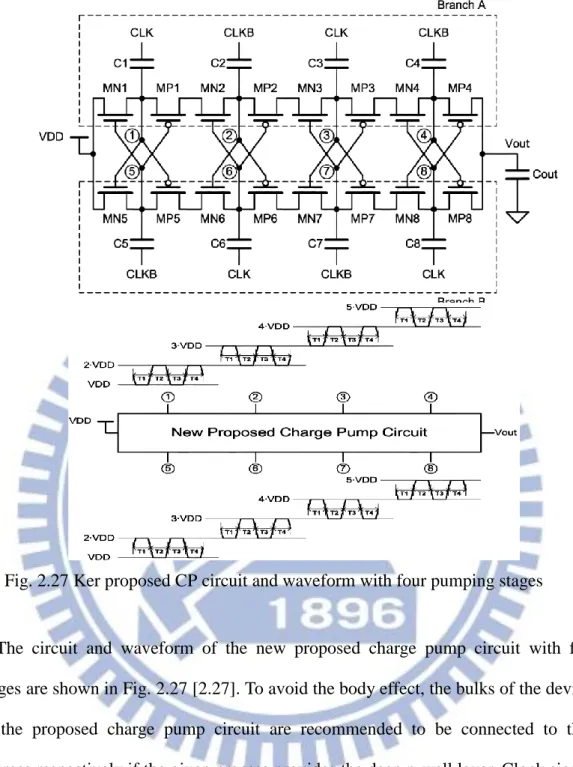
Charge Pump Circuit
Fig. 2.26 shows the four-stage Dickson charge pump circuit, where the
diode-connected MOSFETs are used to transfer the charges from the present stage to
the next stage [2.25] [2.26]. The voltage difference between the drain terminal and the
source terminal of the diode connected MOSFET is the threshold voltage when the
diode-connected MOSFET is turned on. Therefore, the output voltage of the
four-stage Dickson charge pump circuit has been derived as
(2.7)
Fig.2.26 Dickson charge pump circuits
The threshold voltage (Vt) of the diode-connected MOSFET becomes larger due to
the body effect when the voltage on each pumping node is pumped higher. Therefore,
the pumping efficiency of the Dickson charge pump circuit is degraded by the body
25
Fig. 2.27 Ker proposed CP circuit and waveform with four pumping stages
The circuit and waveform of the new proposed charge pump circuit with four
stages are shown in Fig. 2.27 [2.27]. To avoid the body effect, the bulks of the devices
in the proposed charge pump circuit are recommended to be connected to their
sources respectively if the given process provides the deep n-well layer. Clock signals
CLK and CLKB are out-of-phase but with the amplitudes of VDD.
2.5 Previous Low Voltage SRAM Design
2.5.1 SRAM Bit-cell
Differential VSSM 7T SRAM Bit-cell
The standard non-isolated read and writes 2-port 8T SRAM bit-cell is shown in
26
isolated read-port comprising of two transistors M1R, M2R, and a single read bit-line to
directly sense the data from node Q. By separating write port consisting of a single
ended write bitline and write word-line , this design offers a static-noise-margin-free
read operation, since it isolates the read current path (shown in dotted) from the data
storage nodes (Q or QB).
In the reason of separating R/W ports, the isolation of read-ports provides more
than 2 times better read SNM that cannot be achieved in standard 6T bitcell like the
HSNM.
Fig. 2.28 (a) The standard 2-port 8T SRAM bit-cell with non-isolated read-port [2.28]
(b) An isolated read-port 7T SRAM bit-cell [2.28]
DCO 8T SRAM Cell Design
In this paper [2.29], the authors try to use two kind core oxide structures for
power reduction and low VCCMIN. A new structure 8T cell with dual core oxide
(DCO) in 45LPG triple gate oxide CMOS process is proposed for high performance
low leakage mobile applications. The DCO 8T SRAM operates under dual voltage
supplies with write assist. Compared to traditional single-end 8T cell, DCO 8T SRAM
showed the same performance with only half the standby leakage, and lower VCCMIN.
The DCO 8T cell is designed in 45nm LPG CMOS process which shows in Fig.
27
normally at 0.9V and 1.1V, respectively. For example, during low voltage operation,
only VddM will be lowered to 0.6V while VddM1 remains unchanged.
Fig. 2.29 Schematic diagram of the DCO 8T SRAM cell with dual VDD [2.29]
Fig. 2.30 DCO 8T cell shows 2x lower leakage at the same read current at 0.9V
comparing to SCO 8T cell [2.29]
Fig. 2.31 Comparison of leakage components between DCO 8T cell and SCO 8T
cell at 0.9V (Q = 1) [2.29]
Fig. 2.30 shows read current vs. standby leakage comparison between these two
cells across process corners. DCO SRAM standby leakage at 0.9V is only 3nA, which
is half of the SCO cell at the same 98uA Iread performance. This is mainly due to the
28
port.Silicon data showed the DCO cell read BL leakage (sub threshold leakage) and
read pull-down gate leakage are dominating leakage source, as shown in Fig.2.31.
A new 2-port SRAM it-cell
In this paper [2.30], a new structure dual-port 6T cell is proposed. Fig. 2.32
combine with assist MOS and more one global WL, there are three merits show in the
list compare with convention dual port design.
1. A new 2-port 6T memory bit-cell and its word-oriented array organization is
proposed to eliminate simultaneous read and write access disturbances due to
column select functionality in neighboring bit-cells or words.
2. The poor read-noise margin and conflicting read-write problems are handled
by isolating the read and write-ports to achieve higher stability margins.
3. The process variation sensitivity analysis shows that the proposed design has
significantly low process variation sensitivity as compared to existing ones,
hence a better parametric yield.
Fig. 2.32 (a) Schematic diagram of the proposed 2-port 6T SRAM bit-cell with
shared read and write assist transistors per word [2.30]
(b) The VTC and SNM obtained from butterfly curve for the standard ST,
7T and proposed 6T SRAM bit-cells [2.30]
Fig. 2.33 shows a 32-bit word-oriented SRAM array organization of the
29
is divided into many parts block for do this feature. Each word also has a
sub-wordline driver to activate the local wordlines, and a set of read and write-assist
transistors. In a word-oriented SRAM array organization, all the bit-cells of a word
are kept together, which facilitates the sharing of read and write-assist transistors.
Not only reasons said before, multi-divide word and bitline techniques are
commonly used to reduce the charging and discharging capacitance of wordlines and
bitlines, or in other words to minimize the read/write delay for improving the array
performance.
Fig. 2.33 A 32-bit word organization of the proposed 2-port 6T SRAM bit-cell to
eliminate simultaneous read/write disturbance problem [2.30]
Fig 2.34 Simultaneous R/W access issues in word-oriented array [2.30]
Fig. 2.34 shows the schematic diagram of a 2-port 6T SRAM bit-cell memory
module, with word-oriented array organization having four n-bit words (A, B, C and D)
arranged in 2-rows and 2-columns. By this way, the cell array can do simultaneous
30
Zigzag 8T-SRAM
Previously 8T/10T has obvious drawbacks of slower write back or wasteful
layout in implementing schemes, even if they are much better than the 6T cell. A
decoupled single-ended 8T (DS8T) [2.32] suffers slower read first and WB due to its
single-ended sensing. The CP10T [2.33] cell has larger area penalty because it uses a
5-poly pitch layout, and suffers degraded write ability due to its serial access-gates.
Decoupled differential 9T (D9T) and 10T cells improve read speed but require large
area. Poorer area-cost effective cells lead to an increasing σVTH due to limited
resorting to transistor upsizing (Fig. 2.37 & Fig. 2.36).
This paper demonstrates for the first time quantitative performance advantages of
a zigzag 8T-SRAM (Z8T) [2.31]. Fig. 2.35 shows cell over the decoupled
single-ended sensing 8T-SRAM (DS8T) with write-back schemes, which was
previously recognized as the most area-efficient cell under large σVTH/VDD
conditions. Since Z8T uses only 1T for each decoupled read-port, faster 2T
differential sensing (D2S) can be implemented within the same area as the
single-ended DS8T. Thanks to D2S, Z8T cell enables much faster R/W speed at
VDDmin than DS8T. For the same VDDmin/speed, Z8T save the cell area by 15%.
Compare with conventional DS8T area is 14% smaller and 53% faster read. In this
work, a low VDDmin can down to 250mV.
31
9T SRAM
Fig. 2.36 Schematic of the proposed 10T SRAM [2.33]
Fig. 2.37 Schematic of the proposed 9T SRAM [2.34]
A New Low Leakage 8T-SRAM
[2.35]
Figure 2.38 shows the architecture of new 8T SRAM cell. It consists of two extra
transistors MNLL and MNWL as compared to conventional 6T SRAM cell.
Transistor MNLL is used to reduce gate leakage while transistor MNWL is used to
make cell SNM free in the zero state. There are three characteristics in this cell design.
First is a novel read ‘’0’’ static noise margin free eight transistors SRAM cell is
proposed that reduces gate leakage power in the zero state. Second, this new high VT
8T SRAM cell reduces total leakage by 60% in zero state at highest temperature.
Finally, new cell improves SNM by 2.2 times as compared to conventional 6T SRAM cell in read operation and standby mode for the case when cell stores logic ‘1’.
32
2.6 Previous Low Power Register File Design
2.6.1 Register File Bit-cell
The Fig. 2.39 shows a RF bit-cell which can work in sub-threshold region [2.36],
the disadvantage is that the read port limits the cell number on bit-line due to a little
fan-in/out. The author replaced the conventional cell with the bottom right cell Fig.
2.40. It provides a solution to reduce the capacitance. However, the speed will
degrade and cause large area in array. In this mux cell design, select one cell of two
will spend an extra time.
A likely design in Fig. 2.41 also uses the same combinational circuit to reduce the
loading on RBL [2.37]. In this paper, the Double-DICE storage element, which reduces
charge sharing and collecting between the sensitive nodes of sensitive pairs in a Dual
Interlocked Cell (DICE) storage cell. If a radiation particle strikes a sensitive node
(drain of a NMOS or a PMOS in off mode), and it loses its charge, the redundant nodes
restore the state of this affected node and prevent an upset in the storage cell logic. The
DICE design provides excellent protection against SEU for sub-micron technologies,
where a single radiation strike results in charge collection at only one node. So the
author combines this cell and reduce fan in technology by two NAND-OR gate to get a
low capacitor design.
In [2.37], he proposed a Dual-DICE design, which interleaves two DICE storage
cells to make them more resistant to upsets caused by charge sharing and creation of
lateral parasitic bipolar transistors in multiple PMOS devices in deep submicron
technologies. The design provides an area savings as compared to the alternative
33
Fig. 2.39 Cell number on one bit-line is small [2.36]
Fig. 2.40 Two bit-cells share one bit-line [2.36]
Fig. 2.41 Cell number on one bit-line is small [2.37]
The IRF design presented several challenges with the large number of multi-ported
registers required to support the four threads in the core [2.38] [2.39]. The design goal
was to satisfy the performance needs with competitive area and power consumption.
Performance-wise, the pipeline requires a read access immediately after a restore
34
The IRF in this design supplies a maximum of three operands per instruction for the
single active thread. Therefore, the read ports for all four threads are merged into a
compact structure with shared read bitlines (Fig. 2.42) to reduce area and power. The 32
entries are folded into two columns with only 16 read cell pull downs on the bitline for
optimal performance and array aspect ratio [2.40].
Fig. 2.42 IRF integrated memory cell circuit diagram [2.39]
Multi-port separation
Due to more efficient wiring and contact sharing, a 2R1W register file cell is ~3 to 4×
smaller than a 4R2W cell (Fig. 2.43), which reduces cell dimensions and thus both
wordline and bitline lengths by nearly a factor of two [2.41] [2.42].
Instead, the 2R1W cell subarray is replicated (with common write operations
35
achieved while still maintaining low word and bitline capacitances. Even with subarray
duplication, the 3 to 4× smaller cell size achieves a near 2× macro-level area reduction
over a traditional 4R2W design. This area reduction also results in a corresponding
decrease in leakage power. Due to reduced read bitline capacitance and smaller drivers,
read power and read bitline latency can both be improved by ~2×. Write power is not
dramatically affected as reduced write bitline capacitance balances subarray
duplication [2.43].
Fig. 2.43 Standard 4R2W split to 2 copies of a 2R1W cell [2.41]
2.7 Summary
In the beginning of this chapter I introduce the power consumption model and
device geometric effect. Nowadays, leakage power is domain the whole chip power
consumption and how to reduce power dissipation is a very important issue. Standby
power and leakage current are discussed in the section 2.1, then CMOS device design
and new technology such as FinFET, High-K metal gate are also introduced. After
that the basic operation of conventional 6T SRAM and introduce the basic concept
and measurement of stability and write ability in SRAM bit-cell. By technology
process scaling down, the process variation is already damage the SRAM cell stability
36
we introduce some new assist technologies for SRAM design or improve SNM, such
as boosting circuit, keeper design and negative BL …etc. Finally, new cell or share
WWL structures for low power purpose are discussed. Besides, new register design
37
Chapter 3
Low Power 2R2W Multi-Port 8Kb SRAM
Design
3.1 Introduction
In this chapter, a new low power 13T 2 Read 2Write (2R2W) multi-port SRAM bit
cell is proposed. Combine with wide range operation and multi-port and multi-port
goodness, it very suit for portable device or mobile phone. A new sharing WBL
structure and cross Y_Cut & X_Cut can help cell more robustness and improve write
ability and WBL driver power Reduction. Negative VVSS technology is embedded for
low voltage write success. Using this technology, a shorter write 1 time is approached.
In order to gain higher bandwidth, multi-port design becomes more important in
media application. No like conventional single port, multi-port SRAM design can do
synchronous or asynchronous operation, because it with two independent ports. Parallel
operation is got more bandwidth at same time, but a new conflict issues must be take
care.
At first, I discuss conventional problem in Chap.3.2. In this section conflict problem will be specific introduced. In Chap3.4, in order to improve write “1”ability, there are two technology used in this design. Single-end write is low power reduction but write
ability is drop compare with convention differential write. By use negative VVSS and
cut off feedback loop can improve write strength Chap. 3.5 shows post layout
simulation, performance and power analysis. The TSMC 40nm general purpose 2R2W
38
3.2 Conventional Dual-Port 8T SRAM
3.2.1 Two Kinds of Access Mode in DP-SRAM
Fig. 3.1 shows conventional dual-port SRAM bit-cell, it has two port can read / write at the same time. Compare with conventional single port design, dual port
structure give designer more control flexible. Dual-port SRAM provides high
bandwidth and asynchronous CLK timing control property. Conflict problem is a very
important in dual-port, there are many technologies to improve the Vmin of
DP-SRAM against a disturb condition [3.1] [3.2].
Fig. 3.1 Conventional 8T dual-port SRAM cell
Fig. 3.2 Different-row access mode [3.2] Conventional 8T Dual-Port B LA BLB B LA _b B LB _b WLB WLA
39
Fig. 3.3 Access in the same row [3.2]
3.2.2 Write and Read Disturb Issue in 8T DP-SRAM
There are two access modes in two port operation, first is different row which will
no disturbed problem [3.3]. Second is two ports access in the same row
simultaneously (Fig. 3.2 & Fig. 3.3). The case 1 (Fig. 3.4): If write for the left cell in
the same row, and read for the right cell. Dummy read is happened for the left side, which is referred to as “write disturbed” The dummy read operation prevents the internal “1” node from begin flipped by BLA, so the write-ability for the left memory.
40
The case 2 (Fig. 3.5): If read for the left cell on the same row, and another read port
is pointed to the right cell. Dummy read operation occurs for the left cell. The internal “0” node is ramped up though BLA, causing a reduction of the cell current. Consequently reduction in the cell in the cell current leads to a read failure due to lack
of BL swing (read disturb).
Fig. 3.5 Read operation disturbed by dummy read in the same row [3.3]
Timing control with CLK skew disturbed on dual-port also discussed in [3.4]. Timing
variation is relative wire line in whole chip, if positive skew or negative skew is
happened, write / read disturbed maybe caused function failed.
3.2.3 Read/Write Conflict of Dual-port
Fig. 3.6 shows new technologies that can solve the conflict problem by using
timing sharing technology [3.5] [3.6]. Normally, Read and write operation is
forbidden at the same time. In conventional design, if read/write is point to the same
bit, large conflict power consumption and it needs more wide WL pulse have to finish
the operation.
![Fig. 2.10 The read-disturb of 6T SRAM in different process [2.17]](https://thumb-ap.123doks.com/thumbv2/9libinfo/8420753.180502/31.892.130.763.359.1039/fig-read-disturb-t-sram-different-process.webp)
![Fig. 2.16 A conditional keeper with INV chain [2.20] Fig. 2.17 A current mirror keeper [2.22]](https://thumb-ap.123doks.com/thumbv2/9libinfo/8420753.180502/36.892.130.812.347.900/fig-conditional-keeper-inv-chain-current-mirror-keeper.webp)
![Fig. 2.22 8T SRAM cell with on-die RWL and WWL boosting [2.23] Fig. 2.23 2SLS can Effective promotion boost ratio [2.23]](https://thumb-ap.123doks.com/thumbv2/9libinfo/8420753.180502/39.892.68.799.207.811/fig-sram-cell-boosting-effective-promotion-boost-ratio.webp)
![Fig. 2.29 Schematic diagram of the DCO 8T SRAM cell with dual VDD [2.29]](https://thumb-ap.123doks.com/thumbv2/9libinfo/8420753.180502/43.892.109.776.177.827/fig-schematic-diagram-dco-sram-cell-dual-vdd.webp)
![Fig. 2.33 A 32-bit word organization of the proposed 2-port 6T SRAM bit-cell to eliminate simultaneous read/write disturbance problem [2.30]](https://thumb-ap.123doks.com/thumbv2/9libinfo/8420753.180502/45.892.73.837.359.941/organization-proposed-sram-eliminate-simultaneous-write-disturbance-problem.webp)
![Fig. 2.37 Schematic of the proposed 9T SRAM [2.34] A New Low Leakage 8T-SRAM [2.35]](https://thumb-ap.123doks.com/thumbv2/9libinfo/8420753.180502/47.892.67.849.109.1112/fig-schematic-proposed-sram-new-low-leakage-sram.webp)
