行政院國家科學委員會補助專題研究計畫
■ 成 果 報 告
□期中進度報告
新式結構與四氟化碳電漿處理在複晶矽薄膜電晶體應用之研究
The Study of the New Structure and CF
4Plasma
Treatment for Poly-Si
TFT’
s
Application
計畫類別:■ 個別型計畫
□ 整合型計畫
計畫編號:NSC
93-2215-E-009-036
執行期間:
93 年 8 月 1 日至 94 年 7 月 31 日
計畫主持人:
雷添福
國立交通大學電子工程研究所教授
成果報告類型(依經費核定清單規定繳交):■精簡報告
□完整報告
本成果報告包括以下應繳交之附件:
□赴國外出差或研習心得報告一份
□赴大陸地區出差或研習心得報告一份
□出席國際學術會議心得報告及發表之論文各一份
□國際合作研究計畫國外研究報告書一份
處理方式:除產學合作研究計畫、提升產業技術及人才培育研究計
畫、列管計畫及下列情形者外,得立即公開查詢
□涉及專利或其他智慧財產權,□一年□二年後可公開查
詢
執行單位:國立交通大學電子工程研究所
中
華
民
國
94 年 10 月 12 日
行政院國家科學委員會專題研究計畫成果報告
新式結構與四氟化碳電漿處理在複晶矽薄膜電晶體應用之研究
The Study of the New Structure and CF
4Plasma Treatment for Poly-Si
TFT’
s
Application
計畫編號:NSC 93-2215-E-009-036
執行期限:93 年 8 月 1 日至 94 年 7 月 31 日
主持人:雷添福
國立交通大學電子工程研究所教授
一、中文摘要
利用複晶矽薄膜電晶體製作畫素元件 及週邊驅動電路並將之積體化於大面積玻 璃基板已是未來製作平面主動式陣列液晶 顯示器(AMLCD’s)的趨勢。本計畫中我們提 出 數 種 改 善 複 晶 矽 薄 膜 電 晶 體 特 性 的 技 術,包括新式四氟化碳電漿對通道缺陷鈍化 修補(passivation)、新元件結構的發展以及金 屬引發側向結晶法(MILC)於非晶矽轉變成 複晶矽的應用。 以新式的四氟化碳(CF4)電漿的表面前 處理可以在低溫環境下有效地將氟(F)導入 複晶矽中,藉以修補複晶矽薄膜中晶體邊界 缺陷,因為矽與氟的強鍵結可以有效的抵擋 元件在高溫及熱載子作用下的劣化,並以此 四氟化碳(CF4)電漿的表面前處理方法來研 究氟鈍化的機制以及其對於低溫複晶矽薄 膜電晶體的電與物理特性的影響。另外,本 計畫完成新式結構側壁浮接閘極結構的複 晶 矽 薄 膜 電 晶 體 (polysilicon thin film transistor with sidewall floating gate),由實驗 結果證實此新式結構之複晶矽薄膜電晶體 是具有汲極遠離閘極結構 (offset TFTs)般低 的通道關閉漏電流(off current)與傳統元件 般高的通道導通電流(on current)。這是因為 具有自我對準輕摻雜汲極/源極(self-aligned source/drain with lightly doped drain)與浮接 閘極耦合(floating gate coupling)結構的元件 能有效降低汲極端電場並抑制漏電流;此 外,元件的製程不需要額外的光罩來,具有 低成本與製程相容的優點。 關鍵詞: 複晶矽薄膜電晶體;四氟化碳電 漿;缺陷鈍化修補;浮接閘極耦合結構;側 壁浮接閘極。Abstract:
Utilizing polycrystalline silicon thin film transistors (poly-Si TFT’s) as on-glass pixel switch element and peripheral driver circuits is the future trend for fabricating active-matrix liquid-crystal displays (AMLCD’s). In this project, we propose several technologies to improve poly-Si TFT’s performance, including new structure development, channel defect passivation by CF4plasma and metal induced recrystallization of amorphous silicon.
A novel passivation technique of poly-Si TFT’s will be demonstrated by employing CF4 plasma treatments for the first time. With fluorine incorporation into the poly-Si layer, the electrical characteristics of the poly-Si TFT’s can be significantly improved. Moreover, the reliability of the CF4 plasma treated poly-Si TFT’s with respect to the hot-carrier stress and bias temperature stress will be investigation, which is due to the fluorine passivation of trap states in the channel region and SiO2/poly-Si interface.
This project also proposes new devices structure for polysilicon thin film transistor (poly-Si TFT) with sidewall floating gate as an offset gated structure in the OFF state, while acting as a conventional nonoffset structure in the ON state. The self-aligned source/drain with lightly doped drain (LDD) and floating gate coupling structure reduces electric field near the drain and improves the leakage current.
Keywords: Polysilicon Thin Film Transistors,
Passivation, CF4 Plasma, Floating Gate C o u p l i n g S t r u c t u r e , S i d e w a l l Floating Gate.
二、緣由與目的
在複晶矽薄膜電晶體中,在通道中的複 晶矽晶體邊界(Grain Boundary)之缺陷將是 影響元件特性的最主要因素。氫電漿處理 (Hydrogenation)是常被用來鈍化(Passivation) 複晶矽薄膜電晶體中的缺陷,經由氫電漿處 理過的複晶矽薄膜電晶體在電性方面有非 常大的改善,但卻衍生了其他問題: 如熱載 子 (Hot Carrier) 與 高 溫 穩 定 度 (Thermal Stability)問題,原因是因為氫與矽的鍵結容 易在熱載子的撞擊或高溫的情況下斷裂,將 會造成元件特性的劣化。 近年來,氟 (F) 與矽(Si)的鍵結能 因為比氫的鍵結能大,因此被認為可應用於 複晶矽薄膜電晶體的缺陷鈍化,很多報告都 提出氟鈍化處理的複晶矽薄膜電晶體在元 件特性與可靠度上有非常大幅的提升。氟鈍 化製程一般最常用的方法是藉由離子佈植 (Ion Implantation) 將氟離子打入複晶矽的薄 膜中來有效的降低通道裡的缺陷。然而離子 佈植的方法並不適合用在超大型基版的主 動式陣列液晶顯示器之製程,且經過離子佈 植後將產生更多的缺陷,這些缺陷必須經過 額外的高溫退火(Annealing)才能去除,不符 合玻璃基版所要求的低溫製程。到目前為 止,並無其他更有效地導入氟離子的方法被 提出;研究發展出一簡單且與現有製程將匹 配的氟鈍化製程有其深切的必要性。 另一方面,漏電對於複晶矽薄膜電晶體 (Poly-Si TFT’s)一個相當重要的問題,此漏 電機制是來自於接近汲極端複晶矽晶體邊 界 缺 陷 的 高 電 場 所 造 成 的 電 場 發 射 效 應 (Field Emission via Grain Boundary Traps by a High Electric Field near the Drain )與汲極引 發晶體邊界位能下降效應( Drain Induced Grain-Boundary Barrier Lowering Effect )。已 經有許多元件結構被用來抑制因汲極電場 所引起的漏電如汲極遠離閘極結構 (Offset TFT’s)[1],輕摻雜汲極結構(Lightly Doped Drain Structures - LDD TFT’s)[2]以及電場引 發汲極結構(Field Induced Drain Structures -FID TFT’s)[3]。在汲極遠離閘極結構 (Offset TFT’s),輕摻雜汲極結構(LDD TFT’s)的輕 摻雜汲極(LDD)區域與電場引發汲極結構 (FID TFT’s)的電場引發汲極(FID)區域會產 生 一 額 外 的 串 聯 阻 抗 使 得 導 通 電 流 (Offset TFT’s) 與電場引發汲極結構(FID TFT’s)中必須加額外的光罩來完成,光罩的 對不準問題就會產生。在一般的輕摻雜汲極 結構(LDD TFT’s)的元件中,有人提出利用 擴大延伸複晶矽閘極寬度到汲極區域上或 大 角 度 離 子 佈 植 於 閘 極 下 方 輕 摻 雜 汲 極 (LDD) 形 成 閘 極 重 疊 於 汲 極 之 上 的 結 構 (Gate-to-drain Overlap) 以抑制熱載子效應 (Hot Carrier Effect),如此可以增加元件的可 靠度(Reliability)。在元件閘極結構方面,複晶矽浮接閘極 間隙壁( Floating Gate Spacer- FGS) 技術是 應用主要閘極(Main Gate-MG)對浮接閘極 (Floating Gate-FG)的電壓耦合效應,可有效 地 降 低 汲 極 電 場 並 抑 制 通 道 關 閉 漏 電 流 (Off-current),使元件具有良好的輸出電流-電壓特性(Output Characteristics) [5]。我們希 望完成的複晶矽薄膜電晶體(Poly-Si TFT’s) 是具有汲極遠離閘極結構(OffsetTFT’s)般低 的通道關閉漏電流(Off-current)與傳統元件 般高的通道導通電流(On-current)[6]。 在本研究中我們首先提出以新式的四 氟化碳(CF4)電漿的表面前處理可以在低溫 環境下有效地將氟(F)導入複晶矽中,藉以修 補複晶矽薄膜中晶體邊界缺陷,因為矽與氟 的強鍵結可以有效的抵擋元件在高溫及熱 載子作用下的劣化,並以此四氟化碳(CF4) 電漿的表面前處理方法來研究氟鈍化的機 制以及其對於低溫複晶矽薄膜電晶體的電 與物理特性的影響。另外,我們提出具有側 壁浮接閘極結構複晶矽薄膜電晶體(Poly-Si TFT’s with Sidewall Floating Gate),利用閘極 對浮接閘極的電壓耦合(Coupling)效應來產 生自我引發輕摻雜汲極(Self-induced Lightly-doped-drain - SI-LDD)以降低汲極端的電場 並減少通道關閉漏電流(Off-current)而不會 使通道導通電流(On-current)明顯減少;預期 成長的複晶矽晶體具有大晶粒低缺陷以及 高載子遷移率的特性,並進一步希望改善短 通道效應所影起的可靠度(Reliability)問題 並能有效抑制浮接基體效應(Floating Body Effect)。 本計畫主要目的是研究四氟化碳(CF4) 電漿對複晶矽薄膜電晶體的影響以及開發 新式側壁浮接閘極結構的複晶矽薄膜電晶 體,藉由電性結果探討複晶矽薄膜電晶體的
三、結果與討論
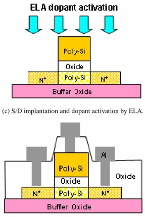
(1) 四氧化氟電漿前處理之準分子雷射複晶 矽薄膜電晶體: 首先我們在晶圓成長一層約 500 nm 的 氧化層,用來模擬玻璃基板。再用低壓化學 氣相沉積(LPCVD)爐管沉積 50 nm 的非晶 矽。以 KrF 準分子雷射退火(Annealing)將此 非晶矽薄膜轉變成複晶矽(Poly Si),此複晶 矽(Poly Si)薄膜即為具有通道與汲極/源極的 元件主動區。利用 RCA 方式清洗晶片後, 利用電漿加強化學氣相沉積(PECVD)系統 做四氟化碳(CF4)的電漿處理。再沉積 50nm 的閘極氧化層薄膜與 200nm 的閘極複晶矽 薄膜。定義閘極,接著以離子佈植植入磷 (Phosphorus)形成 N+汲極/源極區域。並利用 第二次準分子雷射退火(Anneal)來進行摻雜 物 活 化 。 最 後 , 沉 積 400 nm 氧 化 層 (Passivation Layer)並定義接觸窗。再沈積 500nm 的鋁膜並定義成電極。所有製程如 Fig.1 所示:(a) Depositing amorphous silicon and ELA processing.
(b) Defining active region and CF4plasma treatment.
(c) S/D implantation and dopant activation by ELA.
(d) Depositing passivation oxide, opening contact holes depositing metal and patterning.
Fig. 1 Schematic diagram of the fabrication process of poly-Si TFT with CF4plasma treatment.
利用二次離子質譜(Fig.2)我們可以偵測 到在四氟化碳電漿處理的複晶矽裡,有相當 多 的 氟 原 子 累 積 在 閘 極 氧 化 層 及 複 晶 矽 間,我們推測這些氟原子可以有效地修補其 介面缺陷,進而改善電晶體特性。圖二中的 傅立葉轉換紅外光(FTIR)光譜也驗證了複晶 矽中有氟與矽的鍵結(Bonding)。
Fig. 2 SIMS profiles of conventional and CF4plasma-treated
poly-Si films. Inset shows the FTIR spectra of the
conventional and the CF4plasma-treated poly-Si films.
Fig.3 我們比較傳統與經四氟化碳電漿 處理電晶體之轉換特性,我們發現四氟化碳 電漿處後的薄膜電晶體有比較好的開啟電
流(ON-current)較低的關閉電流(OFF-current) 及 較 高 的 電 致 遷 移 率 (Field-effect Mobility)。這些改善最主要來自於氟原子填 補複晶矽中的缺陷。
Fig. 3 Transfer characteristics and field-effect mobility versus gate voltage for the conventional and the CF4plasma-treated
poly-Si TFTs with VDS=0.5V and 5V.
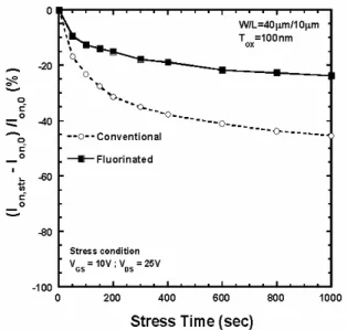
接著,我們利用熱載子測試(Hot Carrier Stress)來檢驗電晶體之可靠度。由 Fig.4 我們 發現未經過四氟化碳處理的薄膜電晶體,其 開啟電流(Ion)非常迅速地劣化,主要是因為 熱 載 子 在 複 晶 矽 通 道 中 撞 擊 出 非 常 多 缺 陷,而使載子的傳輸受到阻礙;然而,經過 四氟電晶處理後,因為矽-氟鍵的強健結能, 有效地抵抗熱載子之破壞,因此有效的提升 薄膜電晶體之可靠度。
Fig. 4 On-current variation as a function of stress time under a
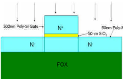
(2) 側壁浮接閘極結構複晶矽薄膜電晶 體: 首先將 P 型晶圓經過標準 RCA 步驟清 洗 後 , 以 濕 氧 方 式 (H2+ O2) 成 長 一 層 約 550nm 的氧化層。利用低壓化學氣相沉積 (LPCVD) 爐 管 沉 積 50nm 的 非 晶 矽 (Amorphous Si),以 600℃,24 小時退火之 固相結晶法(Solid Phase Crystallization-SPC) 將此非晶矽(Amorphous Si)薄膜轉變成複晶 矽(Poly Si)薄膜。 上光阻並利用第一道光罩(mask #1), 把主動區(Active Region)定義出來。利用 RCA 方式清洗晶片後,利用低壓化學氣相沉 積(LPCVD)爐管沉積 50nm 的閘極氧化層薄 膜與 300nm 的摻雜 N 型(N+ in-situ doped)複 晶矽閘極薄膜。上光阻並利用第二道光罩 (mask #2),把閘極(Gate)定義出來,並 以氫氟酸(HF)將汲極/源極區域上方的閘極 氧 化 層 去 除 , 再 以 離 子 佈 植 低 劑 量 磷 (Phosphorus)形成 N-輕摻雜汲極(LDD)。 利用低壓化學氣相沉積(LPCVD)爐管 沉積 50nm 的浮接閘極(FG)氧化層薄膜與希 望的複晶矽浮接閘極薄膜厚度,接著形成預 期寬度的二氧化矽間隙壁(Oxide Spacer)。 利用複晶矽蝕刻系統中複晶矽對二氧 化矽的高蝕刻選擇比,蝕刻未被二氧化矽間 隙壁(Oxide Spacer)所覆蓋的複晶矽浮接閘 極薄膜。以氫氟酸(HF)去除二氧化矽間隙壁 (Oxide Spacer),接著以離子佈植高劑量磷 (Phosphorus)形成 N+汲極/源極(S/D)。利用 低溫長時間退火(Annealing)來進行摻雜物活 化(溫度=600℃, 時間=12hr)。 沉積 550nm 電漿加強化學氣相沉積 (PECVD)鈍化氧化層(Passivation Layer)。上 光阻並利用第三道光罩(mask #3),把接觸 窗(Contact Hole)定義出來。利用金屬物理 氣相沉積系統沈積一層 500nm 的鋁膜來當 作電極。上光阻並利用第四道光罩(mask #4),把金屬電極(Metal Pad)定義出來。所 有製程如 Fig.5 所示:
W/L=10m/10m VD=0.5V, 5V Gate Voltage VG(V) -5 -4 -3 -2 -1 0 1 2 3 4 5 6 7 8 9 10 D r a in C u r re n t I(AD ) 10-12 10-11 10-10 10-9 10-8 10-7 10-6 10-5 10-4 10-3 Conventional TFT SWF-TFT W /L =10m /3.0m VG= 4, 5, 6, 7, 8 V D rain V oltage VD ( V ) 0 1 2 3 4 5 6 7 8 9 10 D ra in C u r re n t I D ( A ) 0 50 100 150 200 250 C o nven tiona l S W F-TF T Fig.6 是元件的轉換特性曲線,由圖可知 傳統結構元件具有較大的漏電流,並且側壁 浮接閘極結構複晶矽薄膜電晶體(SWF-TFT) 具 有 與 傳 統 結 構 元 件 相 差 不 多 的 導 通 電 流;此漏電的主要機制是來自於接近汲極端 複晶矽晶體邊界缺陷的高電場所造成的電 場發射效應,所以側壁浮接閘極結構複晶矽 薄膜電晶體(SWF-TFT) 利用閘極對浮接閘 極的電壓耦合(Coupling)效應來產生自我引 發輕摻雜汲極(Self-induced Lightly- doped--drain - SI-LDD)以降低汲極端的電場並減少 通道關閉漏電流(Off-current)而不會使通道 導通電流(On-current)明顯減少。 Fig.7 是元件的輸出特性曲線由圖可知 側壁浮接閘極結構複晶矽薄膜電晶體較能 抑制 kink 效應並有較大的輸出阻抗,這是因 為 側 壁 浮 接 結 構 能 有 效 降 低 汲 極 電 場 之 故;在沒有明顯犧牲導通電流的情形下,側 壁浮接閘極結構複晶矽薄膜電晶體具有較 飽和的輸出特性曲線,這也表示了浮接基體
Fig. 5 Schematic diagram of the fabrication process of poly-Si TFTs with with sidewall floating gate.
(a) Defining gate and LDD implantation
(b) Depositing sidewall floating gate layer and oxide spacer formation.
(c) Sidewall floating gate formation by selective etching.
(d) S/D implantation and dopant activation.
(e) Depositing passivation oxide, opening contact holes depositing metal and patterning.
Fig. 6 The transfer characteristics of poly-Si TFTs with with sidewall floating gate and conventional TFTs.
Fig. 7 The output characteristics of poly-Si TFTs with with sidewall floating gate and conventional TFTs.
效應(floating body effect)能有效地被抑制並 使得汲極崩潰電壓增加。
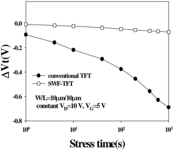
在可靠度方面,我們將元件做熱載子電 應力(hot carrier stress)測試,結果見 Fig.8, 由於傳統結構元件的汲極電場來得比側壁 浮接閘極結構複晶矽薄膜電晶體大,隨著電 應力時間加長,傳統結構元件的臨界電壓的 飄動也隨之變大,反觀側壁浮接閘極結構複 晶矽薄膜電晶體,其臨界電壓的飄動幾乎不 隨著時間增加而有很大的變化。 綜合以上結果,此新結構元件因其漏電 的優異表現能有效地降低功率消耗並且不 會損失元件的導通電流,進而提升元件的使 用壽命而不易劣化。
四、成果自評
本次計畫之執行,皆達預期成果,並已 在相關學術期刊上發表論述,茲列於下: [1] P. Y. Kuo, Tien Sheng Chao, Tan Fu Lei,“Suppression of the floating-body effect in poly-Si thin-film transistors with self-aligned Schottky barrier source and ohmic body contact structure,” IEEE
Electron Device Letters, Vol. 25, no. 9,
pp.634 –636, Sept., 2004.
[2] Shen-De Wang, Wei-Hsiang Lo, Tzu- Yun Chang and Tan-Fu Lei, “A Nove lProcess-Compatible Fluorination Technique with Electrical Characteristics Improvements of
vol. 26, no. 6, pp. 372-374, 2005.
[3] Shen De Wang, Tzu Yun Chang, Chao Hsin Chien, Wei Hsiang Lo, Jen Yi Sang, Jam Wen Lee and Tan Fu Lei, “Performance and Reliability of Poly-Si Thin-Film Transistors on FSG Buffer
Layer,”IEEE Electron Device Lett., vol. 26,
no. 7, pp. 467-469, 2005.
[4] Shen-De Wang, Wei-Hsiang Lo and Tan-Fu Lei, “CF4 Plasma Treatment for Fabricating High Performance and Reliable Solid-Phase-Crystallized Poly-Si TFTs,”
Journal of Electrochemical Society, vol.
152, no. 9, pp. G703-G706, 2005.
[5] Shen De Wang, Tzu Yun Chang, Wei Hsiang Lo, Jen Yi Sang and Tan Fu Lei, “Drain/Gate-Voltage-Dependent On-Current and Off-On-Current Instabilities in Polycrystalline Silicon Thin-Film Transistors underElectricalStress,”Jpn. J.
Appl. Phys., vol. 44, no. 9A, pp. 6435-6440,
2005.
五、參考文獻
[1] K. Tanaka et al, IEEE Electron Device
Lett.1988, pp. 23–25.
[2] C. T. Liu et al. IEEE Electron Device Lett., 1993, pp.149–151.
[3] H. C. Lin et al, IEEE Electron Device Lett., 2001, pp. 26–28.
[4] K. R. Olasupo et al, IEEE Trans. Electron
Devices, 1996, pp.1306–1308.
[5] T .Zhao et al, IEDM Tech Dig., 1993, p.393.
[6] S. Lifshitz et al, IEEE Electron Device
Lett., 1993, pp. 394–396. W/L=10m/10m constant VD=10 V, VG=5 V
Stress time(s)
100 101 102 103
V
t(
V
)
-0.8 -0.6 -0.4 -0.2 0.0 conventional TFT SWF-TFTFig. 8 The threshold voltage variations of conventional TFTs and SWF- TFTs under hot carrier stress.