氮化矽記憶體資料保存行為之數值分析模擬
56
0
0
全文
(2) 氮化矽記憶體資料保存行為之數值分析模擬. Numerical Analysis of the Retention Behavior in Nitride Storage Flash Memory Cells. 研 究 生 : 許智維. Student : Chih-Wei Hsu. 指導教授 : 汪大暉 博士. Advisor : Dr. Tahui Wang. 國立交通大學 電子工程學系 電子研究所碩士班 碩士論文. A Thesis Submitted to Institute Electronics College of Electrical Engineering and Computer Science National Chiao Tung University in Partial Fulfillment of the Requirements for the Degree of Master of Science in Electronic Engineering June 2005 Hsinchu, Taiwan, Republic of China.. 中華民國 九十四 年 六 月.
(3) 氮化矽記憶體資料保存行為之數值分析模擬. 學生:許智維 國立交通大學. 指導教授:汪大暉 博士 電子工程學系. 電子研究所. 摘要. 本篇論文主要探討氮化矽記憶元件內儲存電荷之保存性與穿隧氧化層厚度 之關聯。利用特殊的數值方法並以多層儲存陷井物理模型(multiple trapping model) 分析,來求解 S.R.H.方程式而更精準地提出一種記憶體資料保存行為的表示法。 在 求 解 的 方 程 式 中 , 我 們 用 直 接 穿 隧 (Direct-tunneling) 和 透 過 缺 陷 助 益 穿 隧 (trap-assisted-tunneling)來描述電荷流失的現象,並依據一種對偶的行為–儲存在 缺陷電子經 Frenkel-Poole 激發到傳導帶而傳導帶的自由電子可能被缺陷再捕捉 回去–來說明電荷在氮化矽層的行為。由上述可知,我們的研究將會說明這種自 由電子再被捕捉(recapture)回儲存能態和穿隧現象來決定自由電子的濃度,並隨著 穿隧氧化層厚度增加電荷再被陷阱捕獲行為更加明顯。利用這種再捕捉的行為可 以阻擋電荷流失並增加資料保存的時間。而更深入的探討,在高溫的情況會增加 電荷逃逸,還有穿隧氧化層 stress 效應都將會在這篇論文裡面討論。. i.
(4) Numerical Analysis of the Retention Behavior in Nitride Storage Flash Memory. Student: Chih-Wei Hsu. Advisor: Dr. Tahui Wang. Department of Electronics Engineering & Institute of Electronics National Chiao Tung University. Abstract. The bottom oxide thickness induced the charge loss blocking effect for a SONOS type flash memory is investigated. Utilizing a numerical analysis based on a multiple trapping model for solving the Shockley-Read-Hall (SRH) rate equations, the more accurate expressions for retention behavior are developed. In these equations, the classical tunneling and the stress-induced oxide trap-assisted tunneling mainly accounts for the charge loss and the trapped charge via Frenkel-Poole excitation to conduction band coupled with the conduction free carriers recapture by the traps is used to describe the charge transition within silicon-nitride (SiN) film. The free carrier concentration is governed by two competing processes, tunneling out to Si and recaptured by SiN traps. Our study shows that in an unstressed cell the recapture process starts to dominate as the bottom oxide thickness. ii.
(5) increases. This will block the charge loss and then improve the retention time. In addition, the high temperature enhanced charge escape and the bottom oxide stress effect accelerated data loss have been considered in this thesis.. iii.
(6) 致謝 首先感謝汪大暉教授的指導與淬煉,使我未來在研究上能試著去 解決問題即面對挑戰。 而兩年的研究生涯特別感謝小兔學長的教導。學長帶我實驗的入 門以及碩二一起努力的研究過程,點點滴滴是碩士最深刻的回憶並由 衷感謝在生命的旅程遇到如此好的學長。 此外,旻政學長暗棋的指教和 David 學長在做人及學問方面的模 範都使我獲益良多,並感謝俊威、銘德、志昌學長在操作儀器及問題 討論的幫助。當然,411 LAB 的好伙伴,煥淇、晉輝、晉豪、又仁、 冠德、益輝、靖弘、佑聰、昌樺,由於你們的相伴使得本該枯躁乏味 的研究生活注入了笑聲與活力使大家能撐過這艱辛無比,險惡重重的 碩士兩年。感謝俊榮和至宸學弟在實驗上的幫忙,眾人的協助使這本 對我人生極有意義的論文得以完成。 另外一路走來陪伴在我身邊的好友,羅成、聿弘、昇鴻、明憲、 偉成,你們替我開啟了專業研究的另一扇窗,讓我能更多元的觀看這 個世界,替我的研究生活點綴無數繽紛色彩。 最後,感謝我的父母,是您們無微不至的照顧與時時刻刻的鼓勵 和支持,讓他從青澀叛逆的青春到今有幸完成這本黃皮頁首的碩士論 文,是您們的教導使我脫離徬徨的泥淖而更勇敢堅定的掌握我人生方 向,特別感謝您們能一起見證這段對我自己人生負責的兩年。. iv.
(7) Contents Chinese Abstract English Abstract Acknowledgements Contents Figure Captions Chapter 1 Introduction Chapter 2 Theoretical Model for Data Retention 2.1. Introduction. 2.2. Theoretical Basis 2.2.1 SRH rate equation 2.2.2 Each rate coefficient 2.2.3. 2.3. The component of tunneling current. Simulation model 2.3.1 Assumption 2.3.2 Physical constant and device parameters. Chapter 3. Simulation Method and Numerical Techniques. 3.1. Introduction. 3.2. Numerical method 3.2.1 Explicit and implicit methods 3.2.2 Non-linear and stiff system 3.2.3. The discrete mesh. 3.2.4. Implement numerical implicit method. i ii iiv v vii 1 5 5 5 5 7 10 11 11 13 15 15 15 15 16 18 18. by Newton iteration 3.3. 23. Simulation Flowchart. v.
(8) Chapter 4. Simulation Results of the Retention Behavior in SONOS Memory. 4.1. Introduction. 4.2. Device structure and parameter verification 4.2.1 SONOS structure 4.2.2. 4.3. Calibration of the simulation parameter. Result and discussion 4.3.1 Oxide thickness dependence on gate leakage current 4.3.2. Chapter 5 Reference. Temperature dependence on the charge decay rate. 4.3.3. Nitride trapped charges distribution. 4.3.4. Stress effect. Conclusion. vi. 25 25 25 25 25 28 28 28 35 35 41 42.
(9) Figure Captions Fig. 1.1. Charge injections in SONOS device during (a) +FN write and (b) –FN erase operation. Fig. 1.2. Schematic representation of a SONOS cell and two-bit storage. The shaded area in the nitride layer represents stored charges.. Fig. 2.1. Bandgap diagram of a SONOS device, showing retention loss mechanism: trap-to band tunneling rate (Rt), band-to-band tunneling rate (Rloss), Frenkel-Poole emission rate (Re), and capture rate (Rc).. Fig. 2.2. Fig. 2.2. The trapping range of a SONOS device. The shaded area below Ef represents the filled trap states. Fig. 3.1. (a) The “explicit” forward Euler. (b) The “implicit “ backward method.. Fig. 3.2. The discretized meshes and charge transitions are shown schematically.. Fig. 3.3. (a) The Jacobian matrix structure (b) Each element of Jacobian matrix. J11 is the summation of conduction electrons loss, J1n is the top row of matrix, Jn1 is electron trapping for each mesh and Jnn is the diagonal term Fig. 3.4The flowchart of a simple implicit.. Fig. 3.4. The flowchart of our simulation.. Fig. 4.1. (a) The retention loss of SONOS for 1.8 nm and 1.1 nm bottom oxide at room temperature in Marvin White’s experiment,(b) The retention loss of SONOS for 1.8 nm bottom oxide at room temperature in this experiment.. Fig. 4.2. The retention loss of SONOS with simulation and measurement for 3 nm bottom oxide at room temperature. The simulated data for 3nm thickness is also similar with our measurement data.. vii.
(10) Fig. 4.3. The gate current v.s. read delay time of SONOS for 3 nm, 2.5 nm and 1.8 nm bottom oxide at 298 K, respectively. While the bottom oxide thickness increases, the initial gate leakage current decreases and the corner time increases.. Fig. 4.4. The threshold voltage shift (△Vth) v.s. read delay time of SONOS for 3 nm and 1.8 nm bottom oxide at 298 K.. Fig. 4.5. The currents cased by PF emission and direct tunneling are shown here. The gate current is equal to the combination by IDT and Ithermal.. Fig. 4.6. The mechanism of gate current was shown in this figure. In the beginning, the electrons excited from the shallow nitride traps dominate the leakage. After a period of time, direct tunneling current start to govern the gate current. Fig. 4.7. The percentage of the thermal and DT current was simulated at 1sec. The ratio of the each element to total leakage is investigated as a function of bottom oxide thickness. Fig. 4.8. (a) The measured and simulated retention characteristics of SONOS at various temperature in Marvin White’s experiment. (b) The simulated retention characteristics of SONOS at distinct temperature in this experiment.. Fig. 4.9. The relationship between trap depth and charge density. As the discharge continues, electrons in shallow traps are eliminated earlier than those in deep traps.. Fig. 4.10 The characteristics of charge density distribution in different energy depth. The lower storage density around the interface indicates that the charges near the bottom oxide tunnel out easier than those far away from the interface. Fig. 4.11 The simulation data for various oxide trap densities at zero gate stress bias (Vg=0V). Fig. 4.12 The threshold voltage shift by simulation for various oxide trap densities at zero gate stress bias (Vg=0V). Table 2.1 (a) Universal physical constants and band structure constants (b) Device Parameters for retention simulation model. viii.
(11) ix.
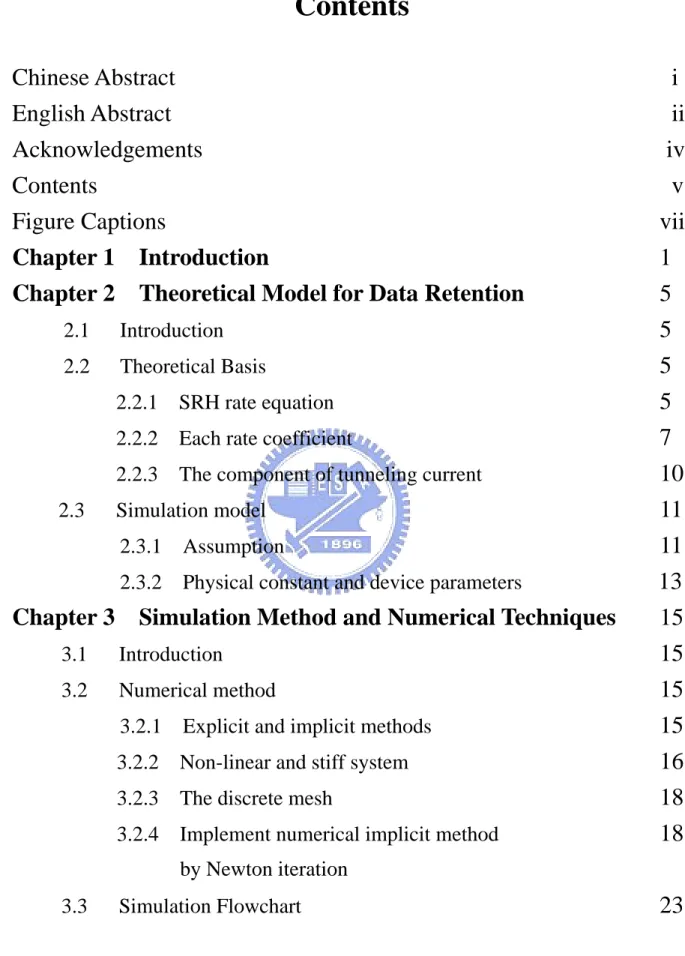
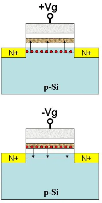
(12) Chapter 1 Introduction. In recent years, great efforts have been invested in nitride-based storage flash memory due to the advantages of the low power, low voltage operation [1][2], the simplicity of the process [3], the ability of continued scaling and the immunity to extrinsic charge loss as compared to the industry standard floating gate flash cell [4]. These type nitride flash cells resemble a standard MOS transistor except that the gate oxide is replaced by an oxide-nitride-oxide gate dielectric stack and can be categorized into uniform storage memory, such as SONOS (positive and negative FN program and erase illustrated in Fig. 1.1), and non-uniform storage memory, such as NROM [5]-[7] (channel hot electron program and band-to-band hot hole erase demonstrated in Fig. 1.2). In addition, SONOS differs from NROM in the bottom oxide thickness. Generally, SONOS memory has a thinner oxide to achieve a high speed of FN programming and erase. However, the data retention has been a critical concern because such thin oxide hardly barricades the charge leakage from the nitride storage node. Therefore, the optimization of the bottom oxide thickness is vital important for amelioration of SONOS technology. Several groups have identified several kinds of charge loss mechanisms in nitride-based devices. Lundkvist et al. described that both the stored electrons direct tunneling to Si and the thermal excitation out from the nitride trap account for retention loss mechanism [8]. Lehovec et al. delivered a simple retention model based on Frenkel-Poole (F-P) release from monoenergetic traps [9][10]. White et al. considered the trap-to-band tunneling combined with the thermal excitation detrapping simultaneously to develop an analytical way to consist with the measurement data [11]. Recently, Wang et al. presented that the nitride charge escapes via F-P emission, followed by a subsequent stress-induced oxide trap assisted 1.
(13) tunneling [12]. Although various physical models have been derived, more conditions should be considered to emulate the retention characteristics accurately. Most models [13] assume that if the charges are emitted to the SiN conduction band, they will be completely emptied out through the ultra-thin bottom oxide (~20Å). This thermal emission enhances the charge decay for a device operated at an evaluated temperature environment. However, for the improvement of the data retention and the minimization of the gate disturb, the thicker bottom oxide is a great solution [14]-[17]. As we know, the tunneling probability decreases exponentially with the increasing the oxide thickness, thereby retarding the charge tunneling out. This would make the assumption that the neglect of tunneling time through the ultra-thin oxide is not applicable for a device with thick oxide. The purpose of this study is to ascertain the bottom oxide thickness dependence on the data retention characteristics of using a numerical simulation. It is suggested that the thicker bottom oxide will block the charge loss, so that the retention behavior can not be expressed by a simple analytical form. For this reason, the multiple trapping models to solve numerically the SRH equations will be introduced. Each loss mechanism for the SONOS memory is illustrated explicitly in Chapter 2. In Chapter 3, the method for our numerical simulation will be interpreted. The implicit backward Euler coupled with Newton iteration is coded within numerical accuracy. In Chapter 4, the simulation and measurement results are compared. Some factors including the temperature dependence, oxide thickness effect, and the stress-induced oxide trap enhanced tunneling are also investigated.. 2.
(14) Fig. 1.1. Charge injections in SONOS device during (a) +FN write and (b) –FN erase operation. 3.
(15) G oxide nitrid e oxide. S n+. Fig. 1.2. D n+. Schematic representation of a SONOS cell and two-bit storage. The shaded area in the nitride layer represents stored charges.. 4.
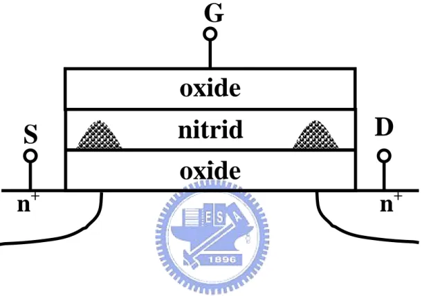
(16) Chapter 2 Theoretical model for data retention 2.1 Introduction In this chapter, the detailed charge transport mechanisms in nitride-based memories were investigated theoretically. In previous research, many groups have proposed the retention loss models neglecting the excited carriers recapture by SiN traps [18] or merely studying the monoenergetic trap level [19][20]. To characterize the accurate decay transient, the recapture events with a multiple trapping states have been taken into account in our model. Here, we adopt the rate equations, based on Shockley-Read-Hall (SRH) theory, describing. electrons. capture,. release. and. tunneling. transitions.. The. Wentzel-Kramer-Brillouin (WKB) approximation as well as trap-like approach depicts the tunneling feature.. 2.2 Theoretical Basis 2.2.1 SRH rate equation The complete charge decay mechanism comprising the tunneling of electrons from trapping site or from SiN conduction band to Si with a series of emission and capture processes is proposed. The four processes are depicted in Fig. 2.1 and the charge transport can be described by two sets cross-coupled SRH rate equations. dnt ( x , φ , t ) = [ Rc ( x , φ , t ) ⋅ nc ( t ) − Re (φ ) ⋅ n t ( x , φ , t )] − Rt ( x , φ ) ⋅ nt ( x , φ , t ) dt. Tn ⋅. (2.1). dnc ( t ) = − ( ∫ ∫ Rc ( x , φ , t ) ⋅ nc ( t )dφdx − ∫ ∫ Re (φ ) ⋅ nt ( x , φ , t )dφdx ) − Rloss ⋅ Tn ⋅ nc (2.2) dt. 5.
(17) φb. Re. Rloss. Rc Rt. SiN. Box. Si. Fig. 2.1. Bandgap diagram of a SONOS device, showing retention loss mechanism: trap-to band tunneling rate (Rt), band-to-band tunneling rate (Rloss), Frenkel-Poole emission rate (Re), and capture rate (Rc).. 6.
(18) Eq. (2.1) is such a change rate for each trapping state concentration and Eq. (2.2) expresses the excess carrier transport in the SiN conduction band. Here, nt and nc are the concentration of occupied and free electrons, x and φ is the distance and energy depth from bottom oxide/SiN interface and from the nitride conduction band edge, respectively. t stands for the retention time and Tn is the thickness of SiN film. The first term on the right-hand in Eq. (2.1) states the capture of the free electrons, the second, F-P emission of the trapped electrons, and the last, direct tunneling of nitride trapped electron to Si. Rc, Re, and Rt are the capture, emission and direct tunneling rate coefficients, separately. Additionally the total trapping states capture and emission transitions are represented at the first and second terms on the right-hand in Eq. (2.2) and Rloss is the loss rate coefficient from nitride conduction. The detailed descriptions for each rate coefficient term are expressed thereinafter.. 2.2.2 Each rate coefficient Time constants have been employed to characterize the electron decay behavior in these discharge process, and the reciprocals of the time constants are defined as the corresponding rate coefficients. Each coefficient will be introduced and formulated. First, the tunneling rate from nitride trap to Si subtrate (trap-to-band) has been derived by a trap-like approach [21], and is described by. Rt = (N C Si ⋅ υth ⋅ σ N ) ⋅ PN ⋅ Pox. (2.3). where N CSi is the Si effective density of state in conduction band, υth is the thermal. velocity, σN is the electron capture cross section of the nitride trap. The quantity of N CSi [22] can be given by. 7.
(19) 2π ⋅ m Si ⋅ kT 3 2 = 2( ) h2 *. N C Si. (2.4). where mSi* is the electron effective mass in Si, k is the Boltzmann constant, and T is the absolute temperature. Pox and PN are the WKB tunneling probabilities through the bottom oxide and the nitride, individually, and are formulated as follows.. Pn = exp{ −. Pox = exp{ −. 4 2qm *n 3hE n. 4 2qm*ox 3hEox. [ φ 3 2 − ( φ − E n ⋅ x) 3 2 ]}. [(φb + φ − En ⋅ x)3 2 − ( φb + φ − En ⋅ x − Eox ⋅ X BO )3 2 ]}. (2.5). (2.6). where φb is the conduction band offset between oxide and nitride, mn*and mox* are the electron effective mass in nitride and oxide, respectively; En and Eox are the average electric field across the nitride and oxide films. Then, the charge loss from nitride conduction band to Si substrate is. Rloss = RTAT + Rtun. (2.7a). RTAT is the trap-assisted-tunneling rate and Rtun is the conventional direct tunneling rate, individually. RTAT can be defined as [23]. 8.
(20) RTAT = υth ⋅ σ ox ⋅ N ox ⋅ PTAT. (2.7b). where Nox is oxide trap density in bottom oxide, σox is the neutral oxide trap capture cross-section and PTAT presents the trap-assisted tunneling probability through the oxide trap. Here, the most favorable trap position is introduced to simplify the PTAT.. PTAT =. P1 ⋅ P2 P1 + P2. (2.7c). It is generally believed that TAT is a two-step tunneling process, i.e. the probability of cathode electrons are first charged by stress-generated traps (P1) and then are immediately discharged out of these neutral traps (P2). In Eq.(2.7a), Rtun expression can be obtained [24]. Rtun =. υth Ptun Tn. (2.7d). Third, the Frenkel-Poole emission rate from nitride traps to conduction band can be written as. Re ( φn ) = (N Cn ⋅ υth ⋅ σ n ) ⋅ exp(. β E n − φn ) kT 9. (2.8a).
(21) where the Frenkel-Poole lowering constant β is given by. β=. q πε o ε n. (2.8b). ε0 and εn are the permittivity of free space and nitride dielectric constant, individually.. Eq. (2.8a) shows that the emission rate has a strong dependence on trap depth and applied electric field, and temperature. Finally, the capture rate of free carriers in nitride conduction to nitride trap is defined as. Rc (x,φn , t) = υth ⋅ σ n ⋅ N t (1 − f ). (2.9). Nt, is the SiN trap concentration per unit energy and f is occupation factor. It is straightforward that the capture rate is proportional to the density of unfilled traps (Nt-nt). .. 2.2.3 The component of tunneling current. Summarized the above equations, the charge leakage current density can be described by the following formula:. 10.
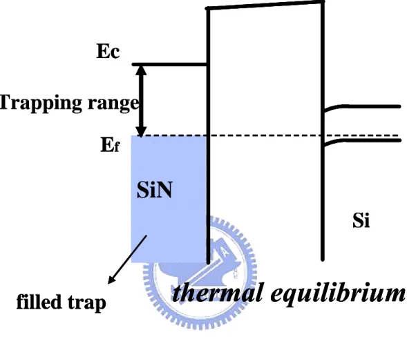
(22) J = ∫∫ Rt (x,φ N ) ⋅ nt (x,φ N , t)dxdφn + q ⋅ υth ⋅ nc ⋅ Ptun ( φb ) + q ⋅ υth ⋅ σ ox ⋅ N ox ⋅ PTAT ⋅ TN ⋅ nc. (2.10). In Eq. (2.10), the entire trapped charge direct tunneling components, non-trap charge tunneling, and trap-assisted tunneling through neutral oxide trap into silicon from conduction band are demonstrated respectively. In the ultra-thin oxide case, the major leakage element is direct tunneling from nitride trapping site to Si substrate. As the bottom oxide thickness and neutral oxide trap density increases, the Frenkel-Poole emission governs the charge decay instead of the direct tunneling [25]. The phenomena will be exhibited in chapter 4.. 2.3 Simulation model 2.3.1 Assumption. In this section, the following assumptions are considered to make our simulation procedure simple and easy to handle. (a) The distribution of trapping range in energy is between SiN conduction band edge (Ec) and the corresponding Si Fermi-level (Ef). This is due to the trap state below Fermi-level is filled under the thermal equilibrium condition, as shown in Fig. 2.2. (b) The trap profile distributes uniformly in trap energy and in space. It is noted that this simplified assumption is sufficient to depict the precise retention behavior. (c) The traps inside the nitride film do not interact with each other due to the misalignment between the trap states. (d) The excited carriers from trapped states to the nitride conduction band are merged together. In other words, the free carrier density above conduction band is irrelevant to the spatial position.. 11.
(23) Ec Trapping range Ef. SiN Si. filled trap. thermal equilibrium. Fig. 2.2. The trapping range of a SONOS device. The shaded area below Ef represents the filled trap states.. 12.
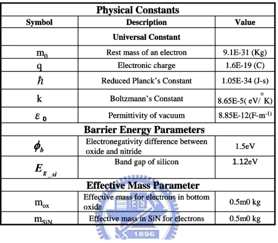
(24) 2.3.2 Physical and Device Parameters. In this simulation, universal physical constants and band structure constants are listed together with the values in Table 2.1(a). The band structure constants encompass energy barrier heights, energy band gaps of silicon , and effective masses for electrons in the oxide and nitride, etc [26]. Device parameters pertain principally to structural parameters like dielectric constants [27] and nitride trapping parameters including capture cross-section [28]. The device parameters are tabulated with the values in Table 2.1 (b). 13.
(25) Table 2.1(a) Universal physical constants and band structure. Physical Constants Symbol. Description. Value. Universal Constant. m0 q. Rest mass of an electron. 9.1E-31 (Kg). Electronic charge. 1.6E-19 (C). h. Reduced Planck’s Constant. 1.05E-34 (J-s). k. Boltzmann’s Constant. 8.65E-5( eV/ K). ε0. Permittivity of vacuum. 8.85E-12(F-m-1). °. Barrier Energy Parameters. φb E g _ si. Electronegativity difference between oxide and nitride Band gap of silicon. 1.5eV 1.12eV. Effective Mass Parameter mox mSiN. Effective mass for electrons in bottom oxide Effective mass in SiN for electrons. 0.5m0 kg 0.5m0 kg. Table 2.1(b) Device Parameters for retention simulation model. Device Parameters Symbol. Description. Value. Dielectric Constants. εN εox Tn TTOP. Static permittivity for Si3N4. 5.7ε0. Static permittivity for SiO2. 3.9ε0. Thickness of SiN layer. 9nm. Thickness of top oxide. 6nm. Trap Parameters σN σox. Carrier capture cross-section for nitride trap Carrier capture cross-section for oxide trap. 5E-13cm2 3E-13cm2. Other Parameters υth β. Thermal velocity. 1E7cm/s. Frenkel-Poole coefficient. 3.17E-4. 14.
(26) Chapter 3 Simulation Method and Numerical Techniques 3.1 Introduction In this chapter, first, the strategy to resolve two cross coupled rate equations for the self-consistent solution is introduced. Based on the implicit and iteration numerical schemes, the two stiff and nonlinear equations in our system can be resolved. The simulation procedure is presented in detail and summarized as a flowchart to achieve convergent solutions and to ensure stability.. 3.2 Numerical method 3.2.1 Explicit and implicit methods Several distinct numerical methods have been applied to solve numerical problems. One of the most applicable methods is “explicit” forward Euler. Here, a concept of explicit is explained by a simple ordinary differential equation.. dy = -λy dt. (3.1). Eq. (3.1) can be transferred to a first order Taylor expression.. y(t + ∆t) − y(t) = − λy(t) ∆t → y(t + ∆t) = y(t) ⋅ (1 − λ∆t). (3.2). In the explicit method, the slope at the time t is employed to determine the increment. 15.
(27) to the function. The advantage of explicit method is a direct computation without solving a complex iteration. However, this method always has a strict limitation on time step size for stability. If the time step, ∆t, is too large, the solution of y(t+∆t) cannot converge toward the steady solution, exhibited in Fig. 3.1(a). Therefore, another “implicit” numerical method which permits the larger time step is required. It uses the unknown information at the time t+∆t to calculate the solution as formula following.. y(t + ∆t) − y(t) = − λy(t + ∆t) ∆t y(t) → y(t + ∆t) = (1 + λ∆t). (3.3). In Fig 3.1(b), the implicit concept is demonstrated and there is no divergent solution compared with Fig 3.1(a). The only concern is that to choose an appropriate time step to reach the precise solution. This will be discussed later. 3.2.2 Non-linear and Stiff system Here, some nomenclatures for our system are given. First, the differential equations in our case are non-linear, containing products of variables. To attain the solution, the Jacobian linearization for non-linear system is essential. In the amorphous material (SiN), one of the eigenvalues is much larger than the others. Such a system is called a “stiff” system of equations. In our case, the release time varying over many orders of magnitude is very short or long compared to the recapture as well as tunneling time. Standard ‘explicit’ scheme is not feasible because only the time steps shorter than the critical time constant are used. To realize the simulation for long-term retention, the time step should be adjustable. For this reason, implicit Euler scheme is adopted to deal with the stiff problem.. 16.
(28) Fig.3.1(a). The “explicit” forward Euler.. Fig.3.1(b). The “implicit “ backward method.. 17.
(29) 3.2.3 The Discrete Mesh Expecting the use of numerical program, the continuous distribution of nitride trap in space and in energy is replaced with discrete approximation. Fig. 3.2 shows schematically the discretized meshes and transitions [29]. The finite difference method obtains an exact site for nt(x,φ) at a finite set of x and φ. First, the traps are treated as a uniform spread in the interval between 0 ≤ x ≤ TN and the distance of each spatial node from bottom oxide/SiN interface is. x i = (i − 1)∆)∆x. i = 1,2,...N. (3.4). where TN is thickness of SiN film and N is the total number of nodes, including those on the boundary. Given TN and N, the each spacing is computed with. ∆x =. TN N −1. (3.5). Similarly, the traps are also assume to distribute uniformly between 0 ≤φ≤ EF and the discretized energy width is. ∆φ =. EF , (p − 1). p = 1,2,...P. (3.6). where EF is the intrinsic Fermi-level of Si substrate under thermal equilibrium and p is the number of the meshes. 3.2.4 Implement numerical implicit method by Newton iteration After describing the discretization manner, an implicit backward Euler solution 18.
(30) φ. . . .. nt(x,φ,t). x Fig.3.2. The discretized meshes and charge transitions are shown schematically.. 19.
(31) conjoint with Newton iteration is selected to provide the required stability for large time step lengths [30], and to reach the steady state solution if the initial guess is reasonable. Prior to the introduction of the simulation procedure, the carrier density variables y(1) and y(N) are labeled, where y(1)=nc, the free electron density y(n)=the trapped electron density (2≤ n ≤ M). and the corresponding M+1 coupled equations for derivative functions f(y) in vector form are listed below.. ⎡ f(y(1)) ⎤ ⎢ f(y(2)) ⎥ dy(n) ⎥ = f(y(n)) = ⎢ ⎢ ⎥ dt M ⎢ ⎥ ⎣ f(y(M))⎦. (3.7). where. − ∑ 2 Rd ( N t − y(n)) ⋅ y(1) dy(1) = f(y(1)) = dx + TN dt Yn. ∑. Yn 2. Re (n) ⋅ y(n) TN. dx − Rloss ⋅ y(1). (3.8). f(y(2)) = Rd ( N t − y(2)) ⋅ y(1) − (Re (2) + Rt (2)) ⋅ y(2). (3.9). M f(y(M)) = Rd ( N t − y(M)) ⋅ y(1) − (Re (M) + Rt (M)) ⋅ y(M). Now, the charge density y at time step number k+1 is denoted by yk+1, Similarly yk is the value at time step k. The implicit first order equation is based on the Eq. (3.10),. 20.
(32) (3.10). y k = y k + 1 − f k + 1 ∆t. where fk+1, denoting f(yk+1(n)), the derivative function vector at the end of the time step, is unknown, but can be found by iteration. By performing a Taylor’s expansion of fk+1, and substituting in Eq. (3.11), the iteration scheme is set up, giving for the (s+1) iterate on the (k+1) step,. (I − ∆t ⋅ J ks + 1 )∆y = ∆t ⋅ f ks+ 1 − y ks + 1 + y k. (3.11). where. (3.12). ∆y = y ks +1 − y ks +1 ,. I is the (M+1) × (M+1) identity matrix and J is the (M+1) × (M+1) Jacobian matrix of partial derivatives with elements:. J ij. ). s. k +1. ∂f = i ∂y j. s. ⎞ ⎟ ⎟ ⎠ k +1. (3.13). The iteration proceeds by solving for Δy and updating ∆y ks +1 to ∆y ks ++11 using 21.
(33) Eq.(3.12), (and hence updating f ks+1 and J ks +1 ) repeatedly until the computed ‘correction’ Δy, is judged to be sufficiently small as the solution converges on the (k+1) time-step value, yk+1. It is useful to consider the structure of the Jacobian matrix in detail, since an effortless simulation and acceptable computer memory is allowed. Fig. 3.3 illustrates the matrix structure. J11 is the summation of conduction electrons loss, J1n is the top row of matrix, Jn1 is electron trapping for each mesh and Jnn is the diagonal term; others are zero. These zero terms mean that the communication between each localized state does not occur.. 3.3 Simulation Flowchart Fig 3.4 shows the flowchart of a simple implicit as well as Newton iteration program suited for the simulation for discharging process. At the outset, the data of the device structure condition, including the discretized mesh size, ONO stack thickness, threshold voltage window, and gate voltage bias, are read. Then, concentration of each trap state at the previous time is loaded, and then the data at next time is evaluated numerically. The output data are judged wether the self-consistent is achieved. If out of the accuracy, the iteration process will continue by decreasing the time step size until the stable results are received.. 22.
(34) Fig.3.3(a). The Jacobian matrix structure. Fig.3.3(b). Each element of Jacobian matrix. J11 is the summation of conduction electrons loss, J1n is the top row of matrix, Jn1 is electron trapping for each mesh and Jnn is the diagonal term. 23.
(35) Fig.3.4. The flowchart of our simulation.. 24.
(36) Chapter 4 Simulation Result of the Retention Behavior in SONOS Memory 4.1 Introduction In this chapter, we will demonstrate the simulation results by utilizing the numerical analysis. First, the device structure is shown and the simulation parameters are examined. Then, the simulated and experimental results are compared and discussed. Finally, the conclusions are drawn.. 4.2 Device structure and Parameter verification 4.2.1 SONOS structure The samples used in this work are n-channel SONOS-type cells. The thickness of each ONO gate stack is 9nm (top oxide, TTO), 6nm (nitride, TN) and a variable bottom thickness, 3nm and 5nm (TBOT). Devices have a gate length of 500µm and a gate width of 500µm. A uniform positive and negative bias is employed for writing and erase, individually. 4.2.2 Calibration of the simulation parameter To ascertain whether the entire simulations are workable, the parameters listed in Table 2.1 should be calibrated. First, the bottom oxide thickness of 1.1nm and 1.8nm are utilized. The two data are consistent with Marvin White’s experimental data, as shown in Fig. 4.1. In addition, the simulated data for 3nm thickness is also similar with our measurement data (Fig. 4.2). All results are gauged at 22oC and the threshold voltage window (∆Vt) is 1.5V. When cells are operated at high temperature (225oC), the decay rate is enhanced and our simulation data can also reflect this phenomenon (Fig. 4.8). We can conclude that the parameters used in our model are reasonable because good agreements can be obtained between simulation 25.
(37) Fig.4.1(a). The retention loss of SONOS for 1.8 nm and 1.1 nm bottom oxide at room temperature in Marvin White’s experiment. [31]. Fig.4.1(b). The retention loss of SONOS for 1.8 nm bottom oxide at room temperature in this experiment.. 26.
(38) Threshold Voltage shift (Volts). 0.0 Simulation data Measurement data. -0.5. 30Å bottom oxide @RT. -1.0 -4 10. -2. 10. 0. 10. 2. 10. 4. 10. 6. 10. Retention Time (sec.) Fig.4.2. The retention loss of SONOS with simulation and measurement for 3 nm bottom oxide at room temperature. The simulated data for 3nm thickness is also similar with our measurement data.. 27.
(39) and measurement results. The detail information will be discussed below.. 4.3 Results and Discussion 4.3.1 Oxide thickness dependence on gate leakage current It is known that thinner bottom oxide has better endurance, while it has poor data retention. Fig. 4.3 shows that as the bottom oxide thickness increases, the initial gate leakage current decreases and the corner time increases. The lower leakage current corresponds to a better charge loss due to a little tunneling transparency through a thicker bottom oxide (Fig. 4.4). Therefore, thickening the bottom oxide is a great solution to improve the data retention. The leakage component combined with thermionic field emission and nitride trap direct tunneling is mentioned in Chapter 2. It is doubtful whether either or both parts control the charge loss simultaneously. In Fig. 4.5, the currents cased by PF emission and direct tunneling are displayed. In the beginning, the electrons excited from the shallow nitride traps dominate the leakage. After a period of time, shallow trapped charges are swept out and this will makes the direct tunneling current start to govern the gate current (Fig. 4.6). As for a thick oxide cell, the current transport in a SONOS cell is due mainly to the PF excitation current as opposed to the direct tunneling current in a thin oxide cell. The measurement is at 1sec and the ratio of the each element to total leakage is investigated as a function of bottom oxide thickness (Fig. 4.7) 4.3.2 Temperature dependence on the charge decay rate In addition to the room temperature (22oC), the memory cells are often situated at different temperature range. According to our model, the gate currents at each temperature are simulated. Fig 4.8 shows the results between simulation and measurement, respectively. It is exhibited that the charge loss at high temperature is accelerated compared with that at a lower temperature. This high temperature will enhance the trapped charge emission rate, thereby degrading the retention behavior.. 28.
(40) Fig.4.3. The gate current v.s. read delay time of SONOS for 3 nm, 2.5 nm and 1.8 nm bottom oxide at 298 K, respectively. While the bottom oxide thickness increases, the initial gate leakage current decreases and the corner time increases.. 29.
(41) Fig.4.4. The threshold voltage shift (△Vth) v.s. read delay time of SONOS for 3 nm and 1.8 nm bottom oxide at 298 K.. 30.
(42) Fig.4.5. The currents cased by PF emission and direct tunneling are shown here. The gate current is equal to the combination by IDT and Ithermal.. 31.
(43) Fig.4.6. The mechanism of gate current was shown in this figure. In the beginning, the electrons excited from the shallow nitride traps dominate the leakage. After a period of time, direct tunneling current start to govern the gate current. 32.
(44) Fig.4.7. The percentage of the thermal and DT current was simulated at 1sec. The ratio of the each element to total leakage is investigated as a function of bottom oxide thickness. 33.
(45) Fig.4.8(a). The measured and simulated retention characteristics of SONOS at various temperature in Marvin White’s experiment. [32]. Fig.4.8(b). The simulated retention characteristics of SONOS at distinct temperature in this experiment.. 34.
(46) The threshold voltage decay rates between 22oC and 225oC are 91mV/dec and 143mV/dec, separately. The two observations consist with our simulation results, 88mV/dec at room temperate and 140mV/dec at high temperature. 4.3.3 Nitride trapped charges distribution The threshold voltage window decreases with the time revolution. This implies that the residual carriers within SiN film also reduce at the same time. To explore the trapped charges distribution between energy and space dimensions, each trap state concentrations at 10-6, 10-1 and 104 seconds for two different temperatures are extracted through simulation process. Fig. 4.9 shows the remaining charge densities at the corresponding energy depth. As the discharge continues, electrons in shallow traps are eliminated earlier than those in deep traps. At a high temperature environment (225oC), more charges are excited due to a higher emission rate coefficient. The “empty-filled” boundary of charge concentration moves deeper compared with that at a lower temperature (22oC). In the spatial direction from bottom oxide/SiN interface toward the gate, the concentrations at different energies under room temperature are demonstrated. As expected, the lower storage density around the interface indicates that the charges near the bottom oxide tunnel out easier than those far away from the interface. Fig. 4.10 shows the result. 4.3.4 Stress effect The aforementioned discussions are only focused on the cells without any stress. In reality, the memory cell always suffers the high electric field, i.e. P/E cycling stress. Here, the capacitor with 5nm bottom oxide thickness is employed. In this regard, the direct tunneling current can be ignored because of the sufficiently small tunneling probability. The major leakage component arises from the trap-assisted tunneling (TAT) current. The traps are neutral and increases with stress condition. At zero gate stress bias (Vg=0V), the simulation data for various oxide trap densities are shown in Fig. 4.11, and the threshold voltage shift is shown in Fig. 4.12. In the initial stage, the limitation of discharging process is the neutral trap density. This will fix the gate. 35.
(47) current level at a certain level. After the corner time, the gate current turns to obey a 1/t time dependence. This is because that the leakage current is limited by the FP excitation and the analytical description is derived at [12].. 36.
(48) Trap depth from CB (eV). Trapped charge density (cm-2·eV-1) 12 12 0 1x10 2x10 t=10-6s. 0.5. 10-1s. 1.0 1.5. 104s. solid: T@225C 2.0 open: T@22C. Fig.4.9. The relationship between trap depth and charge density. As the discharge continues, electrons in shallow traps are eliminated earlier than those in deep traps.. 37.
(49) Fig.4.10. The characteristics of charge density distribution in different energy depth. The lower storage density around the interface indicates that the charges near the bottom oxide tunnel out easier than those far away from the interface.. 38.
(50) Fig.4.11. The simulation data for various oxide trap densities at zero gate stress bias (Vg=0V).. 39.
(51) Fig.4.12. The threshold voltage shift by simulation for various oxide trap densities at zero gate stress bias (Vg=0V).. 40.
(52) Chapter 5 Summary and Conclusion The charge transient behavior in a SONOS type flash memory has been characterized. By a multiple trapping model and two sets cross-coupled SRH rate equations, the charge loss path and the associated components are identified successfully. The Frenkel-Poole emission as well as free carriers retrapping depicts the conduction inside SiN film. And the leakage current is attributed to the loss from the nitride conduction band and trap states. Anticipating the use of numerical analysis, the discretized meshes are required. Utilizing a backward Euler implicit method with Newton’s iteration, the non-linear, stiff equations are solved numerically. This method can enable us to obtain the information at each moment. As the bottom oxide thickness increases, the leakage current is limited for a long time. This phenomenon is referred to “current blocking effect”. The blocking corner time decreases after the cells suffer high field stress. This corner time can be treated as an index of bottom oxide quality. The shorter corner time corresponds to the poorer oxide quality. In addition, at a high temperature environment, the voltage decay will be enhanced due to thermionic field emission. According to simulated trapped charge distribution, the “empty-filled” boundary moves deeper with increasing temperature. It implies that more deep trapped carriers are excited and then accelerating the charge loss.. 41.
(53) Reference [1]. F. R. Libsch and M. H. White,” Charge Transport and Storage of Low Programming Voltage SONOS/MNOS Memory Devices,” Solid-State Electronics Vol. 33, pp. 105-126, 1990.. [2]. Eiichi Suzuki, Hisato Hiraishi, Kenichi Ishil and Yutaka Hayashi, “A Low-voltage alterable EEPROM with Mental – oxide – nitride – oxide – Semiconductor (MONOS) Structures,” IEEE Trans. Electron Devices, pp.122-128, 1983. [3]. M. K. Cho and D. M. Kim, “High Performence SONOS Memory Cells Free of Drain Turn-On and Over Erase: Compatibility Issue with Current Flash Technology,” IEEE Elect. Dev. Lett., Vol.21, pp. 399-401, 2000.. [4] [5]. [6]. M. White, “On the Go with SONOS,” IEEE Circuit and Device Magazine, pp.22-31, 2000. B. Eitan, P. Pavan, I. Bloom, E. Aloni, A. Frommer, and D. Finzi, “NROM: A Novel Localized Trapping, 2–Bit Nonvolatile Memory Cell”, IEEE Elect. Dev. Lett., Vol. 21, pp. 543-545, 2000. B. Eitan, P. Pavan, and I. Bloom, “NROMTM – A New Technology for SONOS. Non-Volatile Memory Products” Solid-State Electronics Vol. 46, pp. 1757-1763, 2002. [7] B. Eitan, “Non-Volatile Semiconductor Cell Utilizing Asymmetrical Charge Trapping”, U. S. Patent 5 768192, June 16, 1998. [8] L. Lundkvist, C. Svensson, and B. Hansson,” Discharge of MNOS Structures at Elevated Temperatures,” Solid-State Electronics, Vol. 19, p.221, 1976. [10] K. Lehovec and A. Fedotowsky, “Charge Retention of MNOS Devices Limited by Frenkel-Poole Detrapping”, Appl. Phys. Lett., Vol. 32, p.335, 1978. [11] M. H. White and J. R. Cricchi “Characterization of thin-oxide MNOS memory transistors” IEEE Trans. Electron Devices, pp.1280-1288, 1972. [12] Tahui Wang, W. J. Tsai, S. H. Gu, C. T. Chan, C. C. Yeh, N. K. Zous, T C. Lu, Sam Pan, and Chih-Yuan .Lu, “Reliability Models of Data Retention and Read-Disturb in 2-bit Nitride Storage Flash Memory Cells (Invited Paper),” IEDM Tech. Dig., pp. 169-172, 2003. 42.
(54) [13] Yu Wang and M. H. White, “An Analytical retention Model for SONOS Nonvolatile Memory Devices in the Excess Electron State,” Solid-State Electronics, Vol. 49, p.97, 2005. [14] W. J. Tsai, N. K. Zous, C. J. Liu, C. C. Liu, C. H. Chen, Tahui Wang, Sam Pan, Chih-Yuan Lu, and S. H. Gu, “Data Retention Behavior of a SONOS Type Two-Bit Storage Flash Memory Cell” IEDM Tech. Dig., pp. 719-722, 2001. [15] Gowrishankar L. Chindalore, C. T. Swift, and David Burnett, “A New Combination-Erase Technique for Erasing Nitride Based (SONOS) Nonvolatile Memories,” IEEE, Elect. Dev. Lett., Vol.24, p.257-259, 2003. [16] Peter C. Y. Chen, “Threshold-Alterable Si-Gate MOS Devices,” IEEE Trans. Electron Devices, pp.584-586, 1977. [17] W. J. Tsai, S. H. Gu, N. K. Zous, C. C. Yeh, C. C. Liu, C. H. Chen, Tahui Wang, Sam Pan, and Chih-Yuan Lu, “Cause of Data Retention Loss in s Nitride-Based Localized Trapping Storage Flash Memory Cell”, Proc. Int. Reliability Phys. Symp., pp. 34-38, 2002. [18] Ross A. Williams and Moiz M. E. Beguwala, ”The Effect of Electrical Conduction of Si3N4 on the Discharge of MNOS Memory Transistors,” IEEE Trans. Electron Devices, Vol. 25, pp.1019-1023, 1978. [19] T. H. Kim, J. S. Sim, J. D.Lee, H. C. Shim, and B. G. Park, ”Charge Decay Characteristics of Silicon-Oxide-Nitride-Oxide-Silicon Structure at Elevated Temperatures and Extraction of the Nitride Trap Density Distribution,” Appl. Phys. Lett., Vol. 85, p.26, 2004. [20] P. C. Arnett, “ Transient Conduction in Insulators at High Fields,” J. Appl. Phys., Vol. 46, pp. 5236-5243, 1975. [21] W. Shockley and W. T. Read,” Statistics of the Recombinations of Hole and Electrons,” Phys. Rev. Vol. 87, p. 835, 1952. [22] Sze, Physics of Semiconductor Devices 2nd Edition, Johb Wiley & Sons Publishers. [23] C. Sevensson, “Trap-assted Charge Injection in MNOS Structures,” J. Appl. Phys., Vol. 44, pp. 4657-4663, 1973. [24] James C. Penley, “Tunneling through Thin Films with Traps,” Phys. Rev. Vol. 43.
(55) 128, p. 596, 1962. [25] P. J. McWhorter, S. L. Miller, and T. A. Dellin, “Modeling the Memory Retention Characteristics of Silicon-Nitride-Oxide-Silicon Nonvolatile Transistors in a Varying Thermal Environment,” J. Appl. Phys., Vol. 68, pp. 1902-1909, 1990. [26] Luca Larcher, Paolo Pavan, and Boaz Eitan, “On the Physical Mechanism of the NROM Memory Erase,” IEEE Trans. Electron Devices, pp.1593-1599,2004. [27] Ross A. Williams and Moiz M. E. Beguwala,” The Effect of Electrical Conduction of Si3N4 on the Discharge of MNOS Memory Transistors,” IEEE Trans. Electron Devices, Vol. 25, pp.1019-1023, 1978. [28] K. A. Nasyro, V. A. Gritsenko, M. K. Kim, H. S. Chae, S. D. Chae, W. I. Ryu, J. H. Sok, J. W. Lee, and B. M. Kim, “ Charge Transport Mechanism in Metal-Nitride-Oxide-Silicon Structures,” IEEE. Elect. Dev. Lett., Vol. 23, pp.336-338, 2002 [29] Gerald W. Recktenwald, Finite-Difference Approximation to the Heat Equation. [30] M. Borissov, N. Kirov, J. M. Marshall, and A. Vavrek, New Physical Problem in Electronic Materials, p.55, 21-29 September, 1990. [31] M. French, H. Sathianathan, and M. White, “A SONOS Nonvolatile Memory Cell for Semiconductor Disk Application,” 5th Nonvolatile Memory Technology Review, Linthicum Heights, Md., p. 70, June 22-24, 1993. [32] Y Yang, M. H. White, “Charge Retention of Scaled SONOS Nonvolatile Memory Devices at Elevated Temperatures. Solid-State Electronics Vol. 44, pp. 948-958, 2000.. 44.
(56) 簡. 歷. 姓名: 許智維 性別: 男 生日: 民國 70 年 08 月 17 日 籍貫: 台灣台北市 地址: 台北市金山南路一段 73 巷 1-4 號 3F 學歷: 私立長庚大學電子工程系. 88.9-92.6. 國立交通大學電子工程研究所碩士班 92.9-94.6 碩士論文題目:. 氮化矽記憶體資料保存行為之數值分析模擬. Numerical analysis of the retention behavior in nitride storage flash memory. 52.
(57)
數據
+3
Outline
相關文件
conduction electron with crystal vibrations transfers the electron's kinetic energy to a valence electron and thereby excites it to the conduction band..
In Section 3, the shift and scale argument from [2] is applied to show how each quantitative Landis theorem follows from the corresponding order-of-vanishing estimate.. A number
2.8 The principles for short-term change are building on the strengths of teachers and schools to develop incremental change, and enhancing interactive collaboration to
If a DSS school charges a school fee exceeding 2/3 and up to 2 & 1/3 of the DSS unit subsidy rate, then for every additional dollar charged over and above 2/3 of the DSS
3.結論-(1)記憶的歷程分為短期記 憶、長期記憶(2)短期記憶經選擇 與複習成為長期記憶(3)短期記憶
- by adding more electrons to Silicon, we decrease the energy that it takes for an electron to reach the conduction band. - this moves the Fermi Level (the highest filled energy
Root the MRCT b T at its centroid r. There are at most two subtrees which contain more than n/3 nodes. Let a and b be the lowest vertices with at least n/3 descendants. For such
proportional to population size” we could say “the relative growth rate is constant.”.. Then (2) says that a population with constant relative growth rate must
