國 立 交 通 大 學
顯示科技研究所
碩 士 論 文
非晶矽薄膜電晶體液晶顯示器閘極驅動電
路之研究
Study of Amorphous Silicon TFT LCD Gate
Driver on Array (GOA) Circuit
研 究 生 :林 俊 傑 Chun-Chieh Lin
指導教授 :劉 柏 村 博士 Dr. Po-Tsun Liu
非晶矽薄膜電晶體液晶顯示器閘極驅動電路之研究
Study of Amorphous Silicon TFT LCD Gate Driver
on Array (GOA) Circuit
研 究 生:林 俊 傑 Student:Chun-Chieh Lin 指導教授:劉 柏 村 博士 Advisor:Dr. Po-Tsun Liu
國 立 交 通 大 學 顯示科技研究所
碩 士 論 文
A Thesis
Submitted to the Display Institute College of Electrical and Computer Engineering
National Chiao Tung University in partial Fulfillment of the Requirements
for the Degree of Master in
Display Institute
July 2010
閘極驅動電路採用非晶矽薄膜電晶體之應用研究
研究生:林俊傑 指導教授:劉柏村 博士國立交通大學顯示科技研究所
摘要
薄 膜 電 晶 體 液 晶 顯 示 器 (thin-film transistor liquid-crystal display,簡稱TFT-LCD)是利用兩片玻璃基板中間夾 雜著一層液晶分子,上層的玻璃基板主要是和彩色濾光片做結合,而 下層的基板則有電晶體嵌於基板上方,當電晶體打開,電流通過電晶 體時會對液晶分子產生電場變化,液晶分子隨著電場變化做不同角度 的偏轉,藉以改變光線的偏極性,配合固定背光源的光度,再透過濾光 片來決定不同畫素的明暗狀態,最後經過彩色濾光片,構成了面板出 現的影像。為了使面板可以顯示正確的影像,一般都是以外部連接的 IC晶片來提供面板所需要的驅動電壓。近年來為了達到輕薄化和節省 成本的目標,採取Gate driver On Array (GOA) 的驅動方法可以有 效的減少外部IC晶片的數量和生產成本。因此,如何以有效率的設計 達成高穩定性,低功率消耗,多功能的GOA電路是目前在正被廣泛研 究的課題。一個電路來達到最小面積的目標,再針對極性反轉的功能設計出第二 的電路,最後提出GOA(III)以實現高穩定性和低功率消耗的電路給高 解析度液晶顯示器使用。而電路是用非晶矽薄膜電晶體(Amorphous Silicon TFTs,簡稱a-Si TFTs)作為電路的驅動元件。雖然非晶矽薄 膜電晶體電子遷移率低,但是它的高均勻性和低成本,是做為產品化 的最優先考量。這三種GOA電路可提供給不同需求的面板,並可實現 高穩定度及高解析度的TFT-LCD。
Application of GOA (Gate driver On Array) Circuit
using amorphous Silicon TFTs
Student:Chun-Chieh Lin Advisor:Po-Tsun Liu
Display Institute
National Chiao Tung University
Abstract
Thin-film transistor liquid-crystal display(TFT-LCD) uses a layer of liquid crystal molecules placed between two pieces of glass, the upper glass is mainly bound with color filters, while the transistors are embedded in the top of lower glass, when the transistor is turned on, the current which pass through the transistor change the electric field for liquid crystal molecules. With the different variation of electric field, the molecules are rotated for different angles and change the polarity of light. By cooperating with fixed backlight and filters determines the light and dark condition in pixels, finally the light through the color filters produces the image which appears in a panel. In general, external bonding IC chips provide the driving voltages of panel and let the panel shows the correctly picture. In recent years, the driving method of GOA can reduce the numbers of external IC chips and the cost of fabrication
effectively in order to realize the slim and low cost display. Therefore, how to achieve the high reliability, low power and multi-function GOA circuit by effective design is the main subject which is being extensively studied.
In this thesis, three kinds of GOA circuits are proposed to solve the above issues. The first GOA circuit is proposed to achieve the goal of minimum area. Then, the second GOA circuit is designed to realize the function of polar inversion. Finally, the third GOA circuit is proposed to obtain high reliability and low power circuits for high resolution TFT-LCDs. However, the circuits use amorphous silicon TFT, referred to as a-Si TFTs as the driving devices. Although a-Si TFTs has low mobility, the high uniformity and low cost of a-Si TFTs are the priority consideration for mass production. The three type of GOA circuits provide to different requirement of panel and achieve the goal for high reliability and high resolution TFT-LCDs.
誌
謝
首先要誠摯的感謝指導教授劉柏村教授,雖然一開始對此專業領 域是處於陌生的狀態,但老師還是細心的教導著,使我得以在面板技 術和元件物理的領域有了更深一步的認識及興趣。在兩年的碩班生涯 中,由於實驗室完整的資源及老師對學問的嚴謹,使我可以將研究做 得更加實際,而非只是閉門造車,使我在這些年中獲益匪淺。 在實驗的過程中我非常感謝可以與實驗室的好夥伴們一起打拼。 和個性非常開朗的鄭光廷修習電子所電路相關課程中總是充滿他的 招牌笑聲,使我忘記修課的辛苦。實力十分堅強的傅治翔總是考試前 幫我解答許多問題,在此對他們兩位同學謹申謝意並且祝福他們在未 來的博士生涯一定會有許多突破性的貢獻。林敬儒無厘頭又十分經典 說話方法,也讓我留下許多深刻的回憶。李富海不虧是有交大羅納度 的稱號的男人,每次看他上場踢球,總是讓我對他高人一等的球技讚 嘆不已。此外也十分感謝立煒、一德、立峯、虛胖、A 爽、阿寶、小 豬學長們指出我研究中的缺失並提供我意見。特別是帶我的竹立煒學 長, 不但以他無比的耐心將他本身豐富的技術知識及有效率的研究 方法教導給我,其幽默風趣的個性更為實驗室生活增添許多色彩。 最後,謹以此論文給我最愛的父母親—林棟盛先生、張美華女士、 我的弟弟—林文傑,感謝家人的鼓勵、特別是父母親多年來辛苦的教 導與栽培,你們默默的支持和關心是我持續前進的最大動力。
Contents
Chinese Abstract………...……….I
English Abstract………...III
Acknowledgements………..V
Contents ………..VI
Figure Captions………...IX
Chapter 1 Introduction 1.1 Background……….11.1.1 Overview of liquid crystal display……….1 1.1.2 Driving system of panel……….…………2 1.1.3 System-on-panel/System-on-glass displays………...3 1.1.4 A-Si technology for LCD industry……….3 1.2 Motivation………...……5
1.3 Thesis organization……….………6
Chapter 2Device of Amorphous Silicon Thin-Film Transistor (a-Si
TFT)
2.1 Measurement of a-Si TFTs………..………..13 2.2 Parameter extraction method……….13
2.3 Model of a-Si TFTs……….……….…..15 Chapter 3 Amorphous Silicon based Gate Driver
3.1.1 Circuit schematic and operations………..23
3.1.2 Simulation results and discussions………25
3.1.3 Measurement setup………26
3.1.4 Measurement result and summary………....27
3.1.5 Summary………..….27
3.2 Low noise tri-operated mode gate driver system…..…….28
3.2.1 Introduction of polarity inversion……….…………28
3.2.2 Circuit schematic and operations …...………..29
3.2.3 Simulation results and discussions………32
3.2.4 Measurement result………..…….34
3.2.5 Summary……….………..34
3.3 Comprehensive gate driver circuit……….…35
3.3.1 Introduction of power issue………..35
3.3.2 Circuit Schematic and Operations……..…………..36
3.3.3 Simulation results and discussions………….……..37
3.3.4 Measurement results………...………..39
Chapter 4 Conclusions
4.1 Conclusions………69
4.2 Future work………...……….70
Figure Captions
Chapter1
Fig. 1.1 Pixel of liquid crystal display……….9 Fig. 1.2 The cross section structure of TFT-LCD panel………..….9 Fig. 1.3 The block diagram of the entire TFT-LCD panel circuits……..10 Fig. 1.4 (a) Panel with bonding IC (b) Panel with SOG and the number of external IC can be reduce………...………..10 Fig. 1.5-The development phases of SOG-LCDs……….11 Fig.1.6 (a)The schematic illustration of the “sheet computer” concept and (b) a CPU with an instruction set of 1-4 bytes and an 8b data bus on glass substrate. ……….….11 Fig. 1.7-The basic GOA circuit and architecture……….12 Fig. 2.1 Cross-section and process flow of a-Si TFT ……….18
Fig. 2.2 Vth is the intersection of ID = 0 and the extended line of
ID VGS = 10V connects to ID VGS = 15V ………...19
Fig. 2.3 (a) Comparisons of IDVD between measurements and models……… 20 Fig. 2.3 (b) Comparisons of IDVD between measurements and models……….21 Fig. 3.1 Schematic of (a) the first proposed circuit GOA (I) cell and (b) corresponding control signals and output………..………..40
Fig. 3.2 Architecture of the first proposed circuit GOA (I)………..41 Fig. 3.3 The simulation result of node A(n) with different decoupling capacitance………...………41 Fig. 3.4 The simulation result of outputs……….42 Fig. 3.5 The fabricated on-panel circuit for GOA and the corresponding measurement setup………...43 Fig. 3.6 Schematic of the GOA (Thomson’s scheme) cell………...……43 Fig. 3.7(a) The layout of fabricated GOA (I), (b) The die photo of fabricated GOA (Thomson’s scheme)……….…….44 Fig. 3.8 Measurement result of (a)GOA (I) (b) GOA (Thomson’s scheme) ……….……….45 Fig. 3.9The four type of polarity inversion……….……….47 Fig. 3.10 The two kinds of two pulse scanning waveforms for corresponding polarity inversion. ………...……….48 Fig. 3.11 The schematic diagram of the second proposed gate driver circuit GOA(II). ………..……….49 Fig. 3.12. (a) The timing diagram of proposed circuit and (b) Waveform variation of A(n) and B(n)………..……..50 Fig. 3.13 The timing chart and output waveform for dot inversion mode……….51
Fig. 3.15 Architecture of the proposed GOA (II) for frame inversion mode……….52 Fig. 3.16 The block diagram of the proposed gate driver with tri-operated modes……….…..52 Fig. 3.17 The simulation waveforms of GOA(II) from 1st, 2nd, 3th and 4th stage with (a) Normal mode, (b) Dot & row inversion mode, and (c) Frame & column inversion mode……….………54 Fig. 3.18 The simulation waveforms of (a)A(n) and Out(n) (b)A(n) and clk ………56 Fig. 3.19 The schematic diagram of the GOA(II) with increasing aspects. ………..57 Fig. 3.20 The layout of fabricated GOA (II)………...…….58 Fig. 3.21 The output waveforms of GOA(II) from 1st, 2ed, 3th and 4th stage with (a) Normal mode, (b) Dot inversion mode, and (c) Frame inversion mode……….59 Fig. 3.22 The output waveforms of GOA(II) from 10th, 20th, 30th and 40th stage with (a) Normal mode, (b) Dot & row inversion mode, and (c) Frame & column inversion mode………60 Fig. 3.23 The controlling circuit of noise-free circuit in the conventional GOA ………62 Fig. 3.24 Schematic of (a) the third proposed circuit GOA (III) cell and (b) the corresponding control signals and outputs………63
Fig. 3.25 The simulation waveforms of GOA(III) from 1st, 2nd, 3th and
4th stage………...64
Fig. 3.26 The simulation waveforms of GOA(III) and the comparison with design of Vth drop compensation………65
Fig. 3.27 Schematic of GOV(III)_v which is the GOA(III) replaces C1 by Mc ………...…65
Fig. 3.28 The simulation waveforms of B(n) and the comparison between GOA(III) and GOA(III)_v………...66
Fig. 3.29 The architecture of proposed GOA(III) cell……….67
Fig. 3.30 Layout of proposed GOA(III) cell………...….67
Chapter 1
Introduction
1.1 Background
1.1.1 Overview of liquid crystal display
The appearance of traditional monitors which called cathode ray tube (CRT) is hard to find nowadays. The multi-kind of flat-panel display technology are invented and developed to make our life more splendid. Among such advanced technology, thin film transistor liquid crystal display (TFT-LCD) [1] [2] [3] [4] is the most well-established one. LCD displays have two areas of polarizing substance, and a liquid crystal solution in between, as shown in Fig. 1.1.With the passing of electric current through the liquid, the crystals line up in such a way that light cannot infiltrate them. Each crystal acts like a shutter, either blocking the light or allowing it to come through. However, the liquid crystal molecules needs to be controlled when different image data inputs, that is, thin film transistors play the role for overall LCD panel. The total cross section structure of TFT-LCD panel is shown in Fig. 1.2 particularly. It can be roughly divided into two part, TFT array substrate and color filter
substrate, by liquid crystal filled in the center of LCD panel. We still need a backlight module including an illuminator and a light guilder since liquid crystal molecule cannot light by itself. However it usually consumes the most power of the system, some applications such as mobile communications try to exclude or replace it from the system. In TFT array substrate, we need a polarizer, a glass substrate, a transparent electrode and an orientation layer. In color filter substrate, we also need an orientation layer, a transparent electrode, color filters, a glass substrate and a polarizer. Most transparent electrodes are made by ITO, and they can control the directions of liquid crystal molecules in each pixel by voltage supplied from TFT on the glass substrate. Color filters contain three original colors, red, green, and blue (RGB). As the degree of light, named “gray level”, can be well controlled in each pixel covered by color filer, we will get more than million kinds of colors on the display.
1.1.2 Driving System of panel
Fig. 1.3 shows the driving system of TFT-LCD panel and the introduction of blocks as following: Timing controller is the operation center of panel. First, the input image data transform to the type of data
corresponding signals by the control signals from the timing controller. The scan driver drives the gate lines and made the switches of pixel are sequential turned on at the appropriate time. The data driver writes the image data in the corresponding pixel by coordination of scan driver and data driver. The voltage converter provides different voltage value to each circuit block.
1.1.3 System-on-Panel/System-on-glass Displays
TFT-LCD technology has some features of system integration within a display. It can make a compact, high reliable, high resolution display. System-on-glass (SOG) displays are value-added displays with various functional circuits, including gate driver, DC/DC converter, analog buffer, DAC, voltage reference circuit [5][6][7]. Fig 1.4 (a) and Fig 1.4 (b) indicate the less number of external IC of the panel with SOG. Fig 1.5 shows development phases of SOG-LCDs. Eventually, it may be possible to combine the keyboard, CPU, memory, and display into a single “sheet computer”. The schematic illustration of the “sheet computer” concept and a CPU with an instruction set of 1-4 bytes and an 8b data bus on glass substrate are shown in Fig. 1.6.
1.1.4 A-Si technology for LCD industry
been the dominant backplane technology for active matrix liquid-crystal displays (AMLCDs) because of its low manufacturing cost, compatibility with large-area process, and rather uniform device characteristics. Recently, the application areas of a-Si TFT-LCDs have been expanded into small mobile displays and large-area TV displays, as well as computer applications, such as notebooks and monitors. Integration of driving circuits on TFT glasses could make a-Si TFT-LCDs more competitive due to overall cost reduction, compactness.
However, there are several obstacles to the implementation of a-Si TFT backplanes with integrated gate driver circuits. First, the low carrier mobility of hydrogenated a-Si TFTs causes speed and area limitation of a-Si TFT integrated circuits. And the absence of a PMOS load makes circuit design more difficult because it is impossible to implement complementary circuit structure. Third, high and variable parasitic capacitance due to the non-self-aligned device structure causes signal distortion due to the clock feed-through. Finally, the reliability of a-Si TFTs with stress, that is, degradation of device characteristics with voltage stress and a decrease in ON-current after long operation time, induces error image on display after long using time.
1.2 Motivation
As rapid progress of the application of broadband has prepared environments for accommodating services such as photo and video mails and mobile digital TV on personal/mobile equipment, the display panels are required to offer higher resolution, narrower bezels and more compact modules than hitherto. The GOA is a part of SOG-LCDs system and meets all of the requirements of the display devices for personal/mobile equipment, including narrow bezel and compactness.
The basic GOA circuit is composed of four TFTs and one capacitor [8] in Fig. 1.7. The scan signal of the basic GOA circuit is distorted due to the floating output and the clock feed-through by large parasitic capacitance. Therefore, the methods for reducing clock feed-through effect has presented [9][10]. This manner makes the output shorts to the voltage of off by pull-down TFTs. Although the solution decreases the feed-through effectively, the reliable problem accompanies by this solution. Because, the pull-down TFTs sustain DC stress all the time, and induce deterioration of device characteristics. Finally, the circuits fail by lowing on-current and large threshold voltage. Hence, the concept of using multi pull-down TFTs to divide the stress time is proposed [11]12][13][14]. However, these methods are has static power consumption when the stage of GOA is operation. In this thesis, we
propose novel GOA circuit without static power consumption. Furthermore, many issues of driving ability, area, number of external signals, yield rate and driving methods are extensively studied [12][15]-[20]. Therefore, the other two concepts of area and polarity inversion issues are also discussed in this thesis.
1.3 Thesis organization
Chapter 1 Introduction
1.1 Background……….1
1.1.1 Overview of liquid crystal display……….1 1.1.2 Driving system of panel……….…………2 1.1.3 System-on-panel/System-on-glass displays………..3 1.1.4 A-Si technology for LCD industry……….3 1.2 Motivation………...……5
1.3 Thesis organization……….………6
Chapter 2Device of Amorphous Silicon Thin-Film Transistor (a-Si
TFT)
2.1 Measurement of a-Si TFTs………..………..13 2.2 Parameter extraction method……….13
3.1.1 Circuit schematic and operations………..23
3.1.2 Simulation results and discussions………25
3.1.3 Measurement setup………26
3.1.4 Measurement result and summary………....27
3.1.5 Summary………..….27
3.2 Low noise tri-operated mode gate driver system…..…….28
3.2.1 Introduction of polarity inversion……….…………28
3.2.2 Circuit schematic and operations …...………..29
3.2.3 Simulation results and discussions………32
3.2.4 Measurement result………..…….34
3.2.5 Summary……….………..34
3.3 Comprehensive gate driver circuit……….…35
3.3.1 Introduction of power issue………..35
3.3.2 Circuit Schematic and Operations……..…………..36
3.3.3 Simulation results and discussions………….……..37
3.3.4 Measurement results………...………..39
Chapter 4 Conclusions
4.1 Conclusions………69
4.2 Future work………...……….70
Fig. 1.1 Pixel of liquid crystal display
Fig. 1.3 The block diagram of the entire TFT-LCD panel circuits [4]
(a) (b)
Fig. 1.4 (a) Panel with bonding IC (b) Panel with SOG and the number of external IC can be reducing.
Fig. 1.5-The development phases of SOG-LCDs[5].
(a) (b)
Fig. 1.6 (a)The schematic illustration of the “sheet computer” concept and (b) a CPU with an instruction set of 1-4 bytes and an 8b data bus on glass substrate[25,26].
Chapter 2
Device of Amorphous Silicon Thin-Film
Transistor (a-Si TFT)
2.1 Measurement of a-Si TFT
Fig. 2.1 and Table 2.1 show a process flow and a schematic diagram of a cross-section of the bottom-gate top-contact amorphous a-Si TFT. The device electrical properties were measured by a Keithley 4200 IV
analyzer in a light-isolated probe station at room temperature. In IDS-VGS
measurement, the typical drain-to-source bias was swept from VGS = -20
V to VGS = 20 V. In IDS-VDS measurement, the typical drain-to-source bias
was swept from VDS = 0 V to VDS = 20 V.
2.2 Parameter Extraction Method
In this session, we describe the methods of typical parameters
extraction such as threshold voltage (Vth) and field effect mobility (μFE)
2.2.1. Determination of the Vth
Threshold voltage (Vth) was defined from the gate to source voltage
at which carrier conduction happens in TFT channel. Vth is related to the
gate insulator thickness and the flat band voltage.
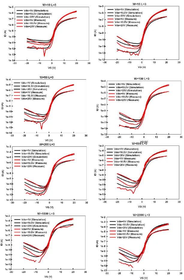
Plenty of methods are available to determine Vth which is one of the
most important parameters of semiconductor devices. This thesis adopts
the method, which is, the intersection of ID = 0 and the extended line
of ID VGS = 10V connects to ID VGS = 15V . Fig 2.2 is the
example of this manner.
2.2.2. Determination of the Field-Effect Mobility
Typically, the field-effect mobility (μFE) is determined from the
transconductance (gm) at low drain bias (VD = 0.1 V). The TFT transfer
I-V characteristics can be expressed as
] 2 1 ) [( C μ = ID FE ox VG Vth VD VD2 L W (2-1) Where
COX is the gate oxide capacitance per unit area,
W is channel width,
If VD is much smaller than VG – VTH (i.e. VD << VG – Vth) and VG >
Vth, the drain current can be approximated as:
D th G V V V L W ) ( C μ = ID FE ox (2-2)
The transconductance is defined as:
D V L W ox FE m=μ C g (2-3) Thus, m D OX g WV C L μFE (2-4) Similarly, we get mobility in the saturation region as
2 ( D) ox G L I WC V
(2-5)2.3 Model of a-Si TFTs
The models for simulation are implemented by a-Si TFTs. The extracted parameters are based on the device size of a-Si TFTs at 25℃.
The field-effect mobility of a-Si TFTs is 0.369 cm2/V∙s. The threshold
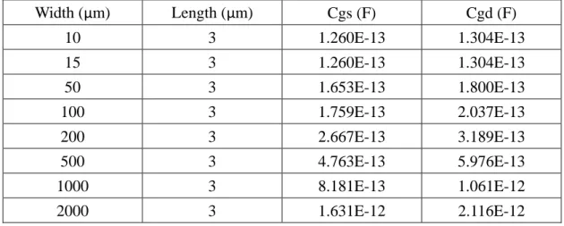
voltage of a-Si TFTs is 4.019 V. In order to higher accuracy of simulation, we use the different model to fitting corresponding width. Fig 2.3 shows the comparison fitting results between simulation and experiment which are very consistent. The TFT models have to add the parasitic capacitance for accurately simulation result and the capacitances are shown in Table 2.2. Finally, the parameters of spice models are demonstrated below:
*****************************************************
****** w=15 l=3 *******
.model NTFT15 NMOS (level=61 vto=-2.5 tox=4e-7
+ alphasat=0.775 gamma=0.68 kvt=-2.36 kasat=0.006 v0=0.11 rs=6000 rd=6000 vaa=710000
+ emu=1.56 sigma0=1e-13 el=0.035 vgsl=3.4 vdsl=7 iol=0.5e-13 vfb=-1 + delta=7 vmin=0.6 gmin=20e22 muband=0.036
+ m=4 lambda=1e-4 epsi=7.5 tnom=27) ******************************* ****** w=50 l=3 *******
.model NTFT50 NMOS (level=61 vto=-2.5 tox=4e-7
+ alphasat=0.775 gamma=0.68 kvt=-2.36 kasat=0.006 v0=0.11 rs=6000 rd=6000 vaa=710000
+ emu=1.56 sigma0=1e-13 el=0.035 vgsl=3.4 vdsl=7 iol=0.5e-13 vfb=-1 + delta=7 vmin=0.6 gmin=20e22 muband=0.035
+ m=4 lambda=1e-4 epsi=7.5 tnom=27) ******************************* ****** w=100 l=3 *******
.model NTFT100 NMOS (level=61 vto=-2.5 tox=4e-7
+ alphasat=0.875 gamma=0.68 kvt=-2.36 kasat=0.006 v0=0.11 rs=6000 rd=6000 vaa=710000
+ emu=1.56 sigma0=1e-13 el=0.035 vgsl=3.4 vdsl=7 iol=0.5e-13 vfb=-1 + delta=7 vmin=0.6 gmin=20e22 muband=0.034
****** w=200 l=3 *******
.model NTFT200 NMOS (level=61 vto=-2.5 tox=4e-7
+ alphasat=0.975 gamma=0.68 kvt=-2.36 kasat=0.006 v0=0.11 rs=6000 rd=6000 vaa=710000
+ emu=1.56 sigma0=1e-13 el=0.035 vgsl=3.4 vdsl=7 iol=1.5e-13 vfb=-0.8 + delta=7 vmin=0.6 gmin=20e22 muband=0.032
+ m=4 lambda=1e-4 epsi=7.5 tnom=27) ******************************* ****** w=500 l=3 *******
.model NTFT500 NMOS (level=61 vto=-2.5 tox=4e-7
+ alphasat=1.075 gamma=0.68 kvt=-2.36 kasat=0.006 v0=0.11 rs=6000 rd=6000 vaa=710000
+ emu=1.56 sigma0=1e-13 el=0.035 vgsl=3.4 vdsl=7 iol=3.0e-13 vfb=-0.3 + delta=7 vmin=0.6 gmin=20e22 muband=0.033
+ m=4 lambda=1e-4 epsi=7.5 tnom=27) ******************************* ****** w=1000 l=3 *******
.model NTFT1000 NMOS (level=61 vto=-2.5 tox=4e-7
+ alphasat=1.075 gamma=0.68 kvt=-2.36 kasat=0.006 v0=0.11 rs=6000 rd=6000 vaa=710000
+ emu=1.56 sigma0=1e-13 el=0.035 vgsl=3.4 vdsl=7 iol=5.0e-13 vfb=-0.3 + delta=7 vmin=0.6 gmin=20e22 muband=0.045
+ m=4 lambda=1e-4 epsi=7.5 tnom=27) ******************************* ****** w=2000 l=3 *******
.model NTFT2000 NMOS (level=61 vto=-2.5 tox=4e-7
+ alphasat=1.075 gamma=0.68 kvt=-2.36 kasat=0.006 v0=0.11 rs=6000 rd=6000 vaa=710000
+ emu=1.56 sigma0=1e-13 el=0.035 vgsl=3.4 vdsl=7 iol=4.0e-13 vfb=-0.3 + delta=7 vmin=0.6 gmin=20e22 muband=0.047
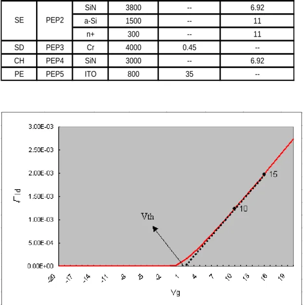
Table 2.1 Film details of a-Si TFT
Fig. 2.2 Vth is the intersection of ID = 0 and the extended line of
ID VGS = 10V connects to ID VGS = 15V
thickness A sheet resistance dielectric constantε
AlNd 2000 0.29 --AlNdN 250 18.84 --SiN 3800 -- 6.92 a-Si 1500 -- 11 n+ 300 -- 11 SD PEP3 Cr 4000 0.45 --CH PEP4 SiN 3000 -- 6.92 PE PEP5 ITO 800 35 --film material SE PEP2 PEP1 GE
Table 2.2 Addition of parasitic capacitance with different size Width (µm) Length (µm) Cgs (F) Cgd (F) 10 3 1.260E-13 1.304E-13 15 3 1.260E-13 1.304E-13 50 3 1.653E-13 1.800E-13 100 3 1.759E-13 2.037E-13 200 3 2.667E-13 3.189E-13 500 3 4.763E-13 5.976E-13 1000 3 8.181E-13 1.061E-12 2000 3 1.631E-12 2.116E-12
Chapter 3
Amorphous Silicon based Gate Driver
3.1 Gate driver with two TFT architecture
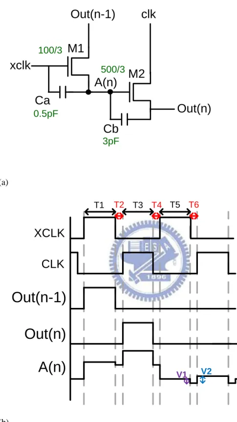
3.1.1 Circuit Schematic and Operations
Fig. 3.1 (a) shows the proposed GOA (I) cell. In the GOA (I) cell, TFTs of M1 and M2 are for generating and shifting scan signals line by line in rows. Out(n) is the output of N-th stage, Out(n-1) is the driver’s output of previous stage or the initial signal from the timing controller (when n=1), clk and xclk are the clock signals from timing controller, Cb is the capacitor of bootstrap and Ca is the decoupling capacitor. In the Fig. 3.1 (b) indicates the corresponding control signals and output of GOA (I). At T1 period, Out(n-1) and xclk change from low to high voltage. Then,
node A(n) is charged to Vdd – Vth1 through M1. Vdd is the highest
voltage from external signal and Vth1 is the threshold voltage of M1.
Furthermore, M2 turns on and Out(n) connects to CLK when the voltage of A(n) is high potential. At T2 period, all external signals become low level and M1 is turned off by xclk. Then, the floating node A(n) still turn on M2. At T2 period, CLK varies from low to high. The node A(n) is
boosted by Cb because M2 charges Out(n) for generating gate line signal. At T4 period, clk become low level and the floating node A(n) still turn on M2. Therefore, Out(n) is discharged to the low state of clk by M2 and closes the corresponding gate line. At T5 period, M1 is turned by the high level of xclk and A(n) discharges to low state of floating Out(n-1). The floating Out(n-1) can’t provide the normal discharging path to make A(n)
connect to off voltage. Nevertheless A(n) discharges to Vlow by
principle of charge share.
Vlow =Cgate line × Out (n−1)+CA (n )× A(n)
Cgate line +CA (n ) ,
CA(n) = Cb + Cgs 2 + Cgd 2 + Ca + Cgs 1
Cgate line and CA(n) are the total capacitance on the gate line and node
A(n) respectively. Cgs is the overlap capacitance between the gate and
source. Cgd is the overlap capacitance between the gate and drain.
Cgate line is generally much bigger than CA(n) and the approximate value of
Vlow = Out(n-1). Out(n-1) is low state at this period. Therefore, the Vlow
can turn off M2 until next frame.
After T5 period, the Out(n) and A(n) must maintain low state in order to avoid the error of gate signal. The error of gate signal means the
TFT is turned by wrong gate line signal. The reason of gate error is the large parasitic capacitor of driving TFT M2 induces the clock feed-through. Then, the gate of M2 raises the value of voltage
V2 = Cgd 2× ∆clk
Cgd 2+Cgs 2+Cb+Cgs 1+Ca . If the voltage of V2 is bigger than Vth2 , and
then M2 is turned on. Hence Out(n) is charged by M2 when clk varied from low to high. For this reason, many kinds of noise-free circuit is proposed to hold the Out(n) at low level, but the noise-free circuit need redundant area. The novel method of GOA (I) is add the decoupling capacitor Ca and connects to xclk. At T6 period, the xclk changes from high to low and induces clock feed-through effect on A(n). Furthermore,
the charging voltage V1 = (Ca+Cgs 1)× ∆xclk
Cgd 2+Cgs 2+Cb+Cgs 1+Ca . V1 is the negative
value. Hence, the maximum of node A(n), A(n)_max = Vlow +V2-V1. If
the value of V2-V1 small than Vth2, M2 always off until the trigger signal Out(n-1) becomes high level.
3.1.2 Simulation results and discussions
The proposed GOA (I) circuit has been designed and verified by the
HSPICE software with the model of Giant Plus in a 3-m amorphous
silicon process. The aspect ratio of channel width (W) to channel length
(L), W/L, for driving transistors M2 are 500m/3m, and switch
and the decoupling capacitor (Ca) are 3pF and 0.5pF, respectively.
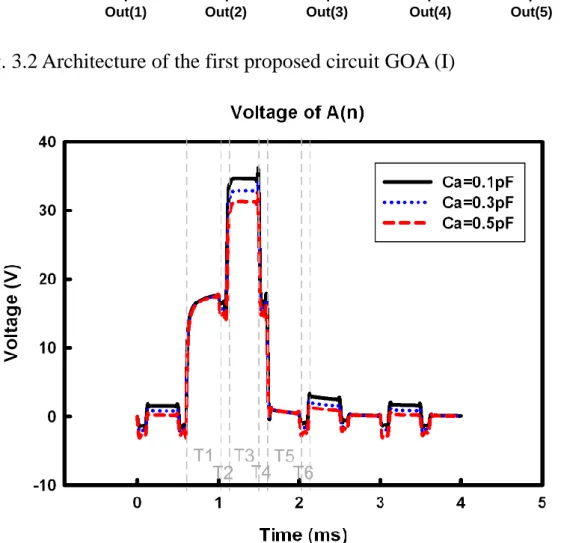
Fig. 3.2 shows the architecture of the proposed GOA (I). In the simulation condition, the voltage range of clk , xclk and In are 0V to 20V and the clock signal’s(clk, xclk) duty is 40%. Fig. 3.3 depicts the simulation result of node A(n) with different decoupling capacitance. In the T3 period, the voltage of A(n) by bootstrap effect is A(n)_T3.
A n T3 = Vdd − Vth − V1 + (Cb+Cgs 2)× ∆Out (n)+Cgs 2× ∆clk
Cgd 2+Cgs 2+Cb+Cgs 1+Ca .
Then, the maximum of A(n) by clock feed through is A(n)_max.
A(n)_max = Vlow+
Cgd 2× ∆clk
Cgd 2+Cgs 2+Cb+Cgs 1+Ca −
(Ca+Cgs 1)× ∆xclk
Cgd 2+Cgs 2+Cb+Cgs 1+Ca
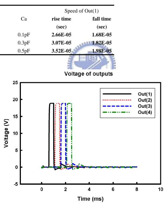
Therefore, A(n)_T3 and A(n)_max become smaller when Ca is increased. If A(n)_T3 is decreased, the speed of GOA becomes slow. Then, the Table 1 and Table 2 indicate this result. Hence, the value of Ca is the tradeoff between speed and stability of gate signal. In this study, GOA (I) chooses the capacitance of Ca is 0.5pF. Fig. 3.4 shows the sequentially output of GOA (I) from one to four stages for first to fourth gate line. Moreover, the fluctuations are small because GOA (I) has the large bootstrap capacitor and suitable decoupling capacitor.
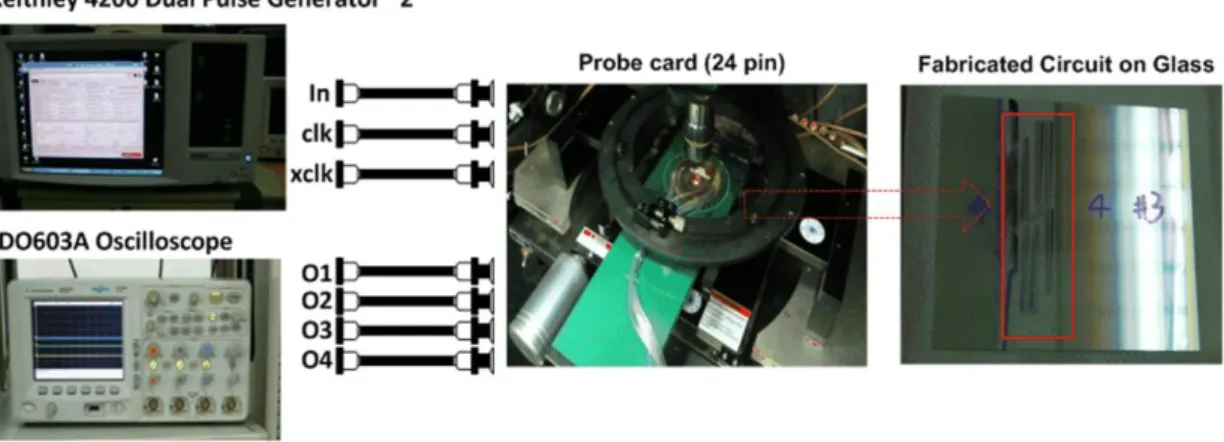
3.1.3 Measurement setup
shown in Fig. 3.5. Then, all signals are transmit by probe card. For circuit verification, the periods of In is 80ms and the periods of clk and xclk are 1ms.
3.1.4 Measurement result
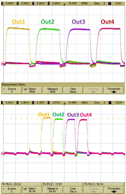
Fig. 3.6 shows the GOA of Thomson’s scheme [8] which is compared with GOA (I). The die photo of fabricated GOA (I) and GOA of Thomson’s scheme are shown in Fig. 3.7 (a) and Fig. 3.7 (b).
Moreover, the area of GOA (I) is 67500 m 2 and smaller than GOA of
Thomson’s scheme due to GOA (I) eliminates all pull-down TFTs. For the measurement setup, the Keithly 4200-scs and digital oscilloscope is utilized as well, the sequentially outputs of GOA (I) and GOA of Thomson’s scheme are shown in Fig. 3.8(a) and Fig. 3.8(b). In Table 3, GOA (I) and prior GOA are have similar root mean square (RMS) value of the voltage fluctuations. This result shows that the node A(n) can be changed and discharged through single TFT M1 by proposed driving method. The GOA(I) provide the stable gate ling signal with just two TFTs.
3.1.5 Summary
In this chapter, GOA (I) provides the concepts of the gate driver cell without pull-down transistors and the methods to reduce output fluctuation. By comparison of prior GOA , GOA(I) reduces 35.71%
layout area and these conclusion are verified in a-Si TFT process.
3.2 Low noise tri-operated mode gate driver
system
3.2.1 Introduction of polarity inversion application
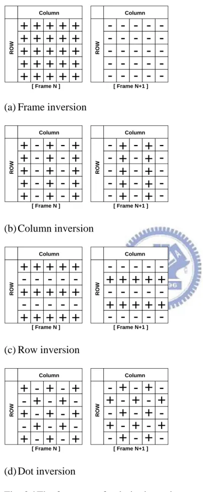
In order to avoid the DC blocking and DC residue effect [4], the driving method of liquid crystal must choose the AC operation. This driving method is called polarity inversion. Fig. 3.9 shows the polarity of voltage which storage in pixel is positive in the frame N. There are changed to negative polarity in the next frame. Then, Fig. 3.9 indicates four type of common inversion mode are frame, column, row, and dot inversion. The average charging time of each pixel becomes shorter for higher resolution of panel. Hence, the pre-charge concepts are proposed and one of the concepts is two pulse scanning [4]. The manner uses the front pulse to pre-charge the corresponding pixel to the same write-in polarity and writes the correctly date by the back pulse. Therefore, the smaller voltage range has to change in the write-in period that means the requirement of write-in time is also reduced. To base on the different polarity inversion, the gate lines need corresponding signals and there are performed in Fig. 3.10.
3.2.2 Circuit Schematic and Operations
(a) Normal mode
In Fig. 3.11, TFTs of M1 to M4 are for generating and shifting scan signals line by line in rows and TFTs of M5 to M6 are for reducing noise fluctuation. Out(n-1) is the driver’s output of previous stage or the initial signal from the timing controller (when n=1), XCLK is the inverse signal of CLK, Out(n) is the output of N-th stage, and Out(n+1) is the output of (N+1)-th stage. Vdd and Vss are the highest voltage and the lowest voltage from external signal, respectively.
Figure 3.12(a) shows the timing chart of the proposed circuit. The operation principle of the gate driver is described as follows. In T1 period, The O(n-1) signal charges the bootstrap capacitor CB by M1 and raises the node A(n) to high level. The voltage of B(n) is discharged to Vss through M6 then turns off M3 and M4 at the same time. Then, M2 is turned on to reset output to a low level. At T2 period, CLK varies from low to high. The node A(n) is boosted by CB because M2 charges Out(n) for generating gate line signal. At T3 period, the path of discharging always has to be performed by M4. Generally M2 and M4 are designed with larger size for pulling up and down the output load. Therefore, layout area can be reduced by shrinking M4. The aspect ratio (W/L) of
falling time and probably produce error of gate line signal because the driving ability of M4 is smaller than M2. The recommended way is to let M2 not only for output charging but also for discharging. In order to implement it, the proposed method is reducing the size of M3 and M5, which can delay the discharging of node A(n). In the Fig. 3.12(b), the dash line of B(n) is charged slowly because of M5 scaling. Node A(n) becomes Vdd+ by coupling effect at beginning of T3 period. Subsequently, M3 is still at off state until B(n) node reaches to Vth level where Vth is the threshold voltage of M3. Therefore, A(n) (dash line) gains a high level duration at T2’ period. At this time, M2 can discharge output from opposite side since TFT is symmetric device. In addition, this method doesn’t have to alter the clock duty and use another logic gates for achieving this driving function [17][21]. Hence the proposed gate driver circuit could operate at simple structure without complicated timing signal and circuit scheme.
(b)Pixel pre-charge for dot inversion mode
In this mode, the circuit schematic is used in Fig. 3.11, which is discussed at above section. Fig. 3.13 shows the timing chart and output waveform for dot inversion mode. The input has to change to IN_2 for generating the scan signal with pre-charge and normal part which are
ground through M6 then turns off M3 and M4. The IN_2 signal charges the capacitor CB through M1 and raises the voltage of node A(1) at the same time. In addition, M2 is turned on to reset output to a low level. In T2 period, A(1) holds at high voltage because of charge conservation and Out(1) is charged to high potential by M2 at the same time, B(n) keeps the low level because XCLK is at the low level. In T3 and T4 period, the circuit repeats the same action as T1 and T2 period. Finally, B(n) is charged by XCLK and turns on M3 and M4 to connect Out(n) to ground level for noise reduction until IN_2 becomes high.
(c) Pixel pre-charge for frame inversion mode
Fig. 3.14 depicts the timing chart and output waveform for frame inversion mode. Same as previous operation, M2 is turned on and copy the clock signal to the corresponding output in T1 to T3 periods. The discrepancy compares to previous mode is that the timing signals CLK__D and CLK2 are double pulse width to original CLK signal. Besides, the timing signal has to change from IN_2 to IN_3 and the signals connect to each stages like Fig. 3.15. According to Fig. 3.14 timing chart, outputs can obtain the waveforms for frame inversion mode.
(d) System control of proposed gate drivers
tri-operated modes. Table 3.4 gives the input relation between the clock connections and operate mode. For required operation mode, the system chooses a group of clock signals and one kind of IN signals. The gate driver stage1 receives the signal from the input stage and begins to generate the corresponding sequential signals to the gate lines based on the circuit schematic in Fig. 3.11. Consequently, the gate diver system has developed a timing control method without output logic block to achieve pre-charge waveform for different polarity inversion by the
proposed TFT gate driver.
3.2.3 Simulation results and discussions
The proposed GOA (II) circuit has been designed and verified by the
HSPICE software with the model of Giant Plus in a 3-m amorphous
silicon process. The aspect ratio of channel width (W) to channel length
(L), W/L, for driving transistors M2 is 600m/3m, pull-down transistors
M4 is 15m/3m, other transistors M3, M5, and M6 are 15m/3m, and
input transistor M1is 100m/3m. Furthermore, the bootstrap capacitor
(Cb) is 3pF.
Fig. 3.17 shows the outputs of gate driver system with different operation modes. Table 3.5 depicts that their speed are very similar with
Although M2 dominates the charging and discharging paths, but the speed of charge and discharge are not symmetrical. Table 3.5 depicts the fall times are smaller than rise time with all operation mode owing to different overdrive voltage. In Fig. 3.18(a), Ta is initial T2 period in Fig. 3.12. Clk charges out(n) via M2 and induce the bootstrap effect on A(n). Then A(n) and out(n) are raised to Vdd++ and Vdd at same time. Because the source of M2 is out(n), the overdrive voltage is Vgs(Ta) – Vth = A(n) – out(n) Vth = Va – Vth. Furthermore, Tb is initial T3 period in Fig. 3.12. The source of M2 is charged to clk and clk is low level at Tb.
Therefore, the Vgs(Tb) becomes Vdd+ Vss = Vb and Vb is bigger than Va. In Fig. 3.18(a) and 3.18(b), the Va and Vb are 14.4V and 26.9V, respectively and the bigger overdrive voltage leads to larger current at Tb. This design makes the GOA has better speed to turn off the gate line and avoids that the pixels write the data of next pixels. However, this speed is not enough to use on panel if the output load is 65pF and 5.2MΩ. The straightforward manner is increase the aspect of driving transistor and
voltage range. Hence, the increasing aspect of M2 is 2000m/3m and
voltage range becomes 25V in Fig. 3.19. Table 3.6 shows the rise time
and fall time becomes 7.5s and 4.8s. Furthermore, the speed can
speed up design in next chapter.
3.2.4 Measurement result
The layout of fabricated GOA (II) cells and the 100 stages gate driver are shown in Fig 3.20(a) and Fig 3.20(b). GOA (I) and GOA (II) have same measurement settings to measure. All outputs of GOA (II) provide sequential gate signals form stage (1) to stage (100) with normal mode in Fig. 3.21 (a). Then, Fig. 3.21 (b), Fig. 3.21 (c), Fig. 3.22 (b), and Fig. 3.22 (c) show the output waveforms with different inversion mode. Table 3.7 and Table 3.8 depict measurement result of GOA (II) and GOA (II) with increasing size and voltage range, respectively. Furthermore, the RMS of fluctuations of GOA (II) are smaller than GOA (I)’s because the noise-free circuit (M3, M4, M5, and M6). The noise-free circuit always pull the output to Vss expect that the output is charging the gate line. These results of measurement are matching the results of simulation and there is shown in Table 3.7 and Table 3.8.
3.2.5
Summary
The proposed gate driver system of GOA (II) can provide different operation mode signal with corresponding input signals and without output logic gate. Moreover, single driving transistor design of GOA (II)
speed. Therefore, GOA(II) is the good solution for the integrated gate driver design for high-resolution panel.
3.3 Comprehensive gate driver circuit
3.3.1 Introduction of power issue
Fig. 3.23 shows he controlling circuit of noise-free circuit in the
conventional GOA [12][13][14]. In general, the width of MD is larger
than ML . When Vx = Vdd, the transfer function is like the inverter,
OUT=IN and is called the pseudo NMOS inverter [22]. The voltage
transfer function shows below:
OUT= IN − Vt − (IN − Vt)2 −WL
WD(Vdd − Vt)
2 at IN=Vx=Vdd.
OUT=Vdd-Vt at IN=0, Vx= Vdd
Therefore, OUT must be the low level when IN is high voltage. For this
reason, the Boolean expression of OUT is equal to Vx × IN . The
noise-free circuit is triggered only at OUT=1 which means Vx is the high voltage and IN is the low level. This is the easy and effective manner to control the noise-free circuit. Nevertheless the drawback is the static power consumption when Vx and IN are high state. In this chapter, the proposed GOA circuits use the novel method to avoid static power consumption, reduce the voltage stress on noise-free circuit and raise the speed of GOA.
3.3.2 Circuit Schematic and Operations
In Fig. 3.24 (a), the third proposed GOA (III) uses transistor M5 and C1 to replace the pseudo NMOS inverter and generates the same Boolean
expression, B(n)= xclk × Out(n − 1) . When xclk and Out(n-1) are high,
the current can’t pass through the capacitor C1 and the B(n) short to Vss by M5. Then, if M5 is turned off by Out(n-1) and xclk changes from low to high level, the B(n) becomes high level by capacitor couple and the
voltage value is C1× ∆xclk
CB (n )+C1. CB(n) is the total parasitic capacitance on node
B(n). However C1 maybe need large area if the Cbn is not enough small.
Therefore, GOA (III) eliminates the source of static power consumption.
In Fig. 3.24 (b) indicates the corresponding waveforms of GOA (III). At T1 period, B(n) is the low level due to Out(n-1) is Vdd. Then, M3, M6, and M7 are turned off by the low voltage of Out(n+1), B(n), and B(n+1), respectively. A(n) is charged to Vdd- by M1 and then A(n) is charged to Vdd by M8. Because the voltage on the gate of M8 is bigger than Vdd at T1 period, the M8 operates at linear region and pass the high voltage to A(n) without Vt drop. The voltage A(n-1) is from the bootstrap
capacitor of last stage and is raised the VH at the same time. Out(n) is
raised to higher voltage VH by the same bootstrap effect. Hence, M2 has
bigger overdrive voltage and operation current. Then, this design makes the GOA (III) has quicker speed. At T3 period, B(n) raises to high level due to the xclk changes from low to high level and Out(n-1) is low level. Then, A(n) is discharged to Vss by M3 and M6. In the meantime, Out(n) is discharged to Vss by M4 due to xclk turns M4 on. After T3 period, Out(n) hold to Vss by two alternately path. One path is M4 and other path is M1and M6 of next stage. Furthermore, A(n) is shorted to Vss by two alternately path of M6 and M7. By two alternately paths, the pull-down transistors suffer the half DC voltage stress and the lifetime can be extended. Therefore, the third proposed GOA (III) has lower power consumption, higher speed, and longer lifetime.
3.3.3 Simulation results and discussions
Fig. 3.25 shows the sequential outputs of GOA(III) and the waveforms are generated by first to fourth stages. Table 3.9 indicates the rise time and fall time of GOA(III). The fall times are shorter than rise fall time by the same reason which in the chapter three. In the first stage (n=1), the gate of M8 should connect to A(0) but the voltage A(0) is not exist. Therefore, the gate of M8 is connected to Out(0) which is input signal from IC. Then the maximum bootstrapping voltage of A(1) is smaller the other stages due to the Vt drop of M8. Fig. 3.26 shows the
different of A(n) between first stage and second stage. The A(2) of second stage has Vt drop compensation design and generates bigger driving ability by higher bootstrapping voltage. Table 3.9 depict the charging and discharging time of second stage are reducing 7.84% and 11.16%, respectively. If every gate lines want to the same speed, the first stage of GOA (III) is the dummy stage and the out (2) is connected to first gate line. In addition, the speed of A(2) change from low to high is also quicker than A(1) because the different charging ability of M8. Therefore, the M8 can reduce the width when the gate connects to A(n-1).
Fig. 3.27 shows the GOA(III)_v cell which is the GOA(III) with varying pseudo NMOS inverter and use the same operation principle. We use this circuit to compare with GOA(III). Fig. 3.28 indicates the B(2) of GOA(III) is similar the square wave and has quicker response time to turn on pull-down TFTs. The GOA(III)_v needs more time to turn on pull-down TFTs because the B(1) is charged through Mc but the B(1) is coupled by C1 in GOA(III). However, the response time is decreased by increase the width of Mc but the static power consumption is also enlarged. Hence GOA(III) has short response time and lower power consumption.
3.3.4 Measurement results
Fig. 3.29 shows the architecture of proposed GOA(III) and this architecture is fabricated on glass in Fig. 3.30. The circuit is also measured by Keithly 4200-scs and oscilloscope. Then, Fig. 3.31 and shows the outputs of GOA(III) and those are not only correctly but also low fluctuation. By the measurement result in Table 3.11, the speed of output1 is slower than other outputs because first stage without Vt compensation. Therefore, the stage with Vt compensation can reduce 36.36% rise time and 18.75 fall time.
3.3.5 Summary
The conventional noise-free circuit has the problem of static power consumption and lifetime. Then, the input of prior GOA can’t pass full range of supply voltage due to the Vt drop. This propose GOA provide the concept of eliminating static power consumption and the methods of expanding life time and speed up. By these manner, the GOA is more suitable for high resolution panel
Ca
0.5pFM1
100/3M2
500/3Cb
3pFclk
Out(n-1)
xclk
Out(n)
A(n)
(a)Out(n-1)
CLK
XCLK
Out(n)
A(n)
T1 T2 T3 T4 T5 T6 V2 V1 (b)Fig. 3.1 Schematic of (a) the first proposed circuit GOA (I) cell and (b) corresponding control signals and output.
Stage1 In Out(1) Stage2 Out(2) Stage3 Out(3) Stage4 Out(4) Stage5 clk xclk Out(5)
Fig. 3.2 Architecture of the first proposed circuit GOA (I)
Fig. 3.3 The simulation result of node A(n) with different decoupling capacitance
Table 3.1 The simulation data of node A1
Voltage of A(1) Ca At T3
period
Maximum by clock feed through
0.1pF 34.6 V 1.74 V
0.3pF 32.9 V 0.898 V
0.5pF 31.3 V 0.267 V
Table 3.2 The simulation information of output1
Speed of Out(1) Ca rise time (sec) fall time (sec) 0.1pF 2.66E-05 1.68E-05 0.3pF 3.07E-05 1.82E-05 0.5pF 3.52E-05 1.98E-05
Fig. 3.5 The fabricated on-panel circuit for GOA and the corresponding measurement setup. CLK M1 M2 M3 M4 Cb Out(n) 600/4 30/4 100/4 30/4 Out(n+1) 2pF Out(n-1)
(a)
(b)
Fig. 3.7(a) The layout of fabricated GOA (I), (b) The die photo of fabricated GOA (Thomson’s scheme)
Table 3.3 (a) Measurement data of GOA(I)
Measurement Rise time (µs) Fall time (µs) RMS of fluctuations (V)
OUT(1) 24 20 0.468
OUT(2) 48 28 0.272
OUT(3) 52 28 0.340
OUT(4) 46 24 0.448
Table 3.3 (b) Measurement data of GOA (Thomson’s scheme) Measurement Rise time (µs) Fall time (µs) RMS of
fluctuations (V)
OUT(1) 54 36 0.559
OUT(2) 50 32 0.451
OUT(3) 48 28 0.472
R O W Column
+ + + + +
+ + + + +
+ + + + +
+ + + + +
+ + + + +
R O W Column[ Frame N ] [ Frame N+1 ]
(a) Frame inversion
R O W Column
+ - + - +
+ - + - +
+ - + - +
+ - + - +
+ - + - +
R O W Column+ +
+ +
+ +
+ +
+ +
[ Frame N ] [ Frame N+1 ] (b) Column inversion R O W Column+ + + + +
-+ -+ -+ -+ -+
-+ -+ -+ -+ -+
R O W Column-+ -+ -+ -+ -+
-+ -+ -+ -+ -+
[ Frame N ] [ Frame N+1 ] (c) Row inversion R O W Column
+ - + - +
+ +
-+ - -+ - -+
+ +
-+ - -+ - -+
R O W Column+ +
-+ - -+ - -+
+ +
-+ - -+ - -+
+ +
[ Frame N ] [ Frame N+1 ] (d) Dot inversion1st gate line 2nd gate line 3rd gate line N-1th gate line Nth gate line Pre-charge pulse Write in pulse
[ For Dot & Row inversion]
[ For Frame & Column inversion] 1st gate line
2nd gate line
3rd gate line
N-1th gate line
Nth gate line
Fig. 3.10 The two kinds of two pulse scanning waveforms for corresponding polarity inversion.
Out(n-1) CLK XCLK M1 M2 M3 M4 M5 M6 Out(n) 600/3 15/3 15/3 100/3 15/3 15/3
A(n)
A(n)
Cb 3pFB(n)
VssFig. 3.11 The schematic diagram of the second proposed gate driver circuit GOA(II).
Out(n-1) CLK XCLK Out(N) Out(n+1) Out(n+2) A(n) B(n) T1 T2 T3 T4 T2' Vdd++ Vdd-(a) B(n) A(n) T2' Vss End of T2 Beginning of T3 Vdd+ Vdd Vss Vdd Vth Vth (b)
Fig. 3.12. (a) The timing diagram of proposed circuit and (b) Waveform variation of A(n) and B(n).
IN_2 XCLK CLK Out(1) Out(2) Out(3) A(1) Vdd+ B(1) T1 T2 T3 T4 T5 T6 T4' pre-charge
Fig. 3.13 The timing chart and output waveform for dot inversion mode.
Fig. 3.14 The timing chart and output waveform for frame inversion mode.
stage1 In_3 Out(1) stage2 Out(2) stage3 Out(3) stage4 Out(4) CLK_D XCLK_D CLK2 XCLK2
Fig. 3.15 Architecture of the proposed GOA (II) for frame inversion mode stage1 Vout(1) stage2 Vout(2) stage3 Vout(3) stage4 Vout(4) CLOCK 1 2 3 4 Vstart Normal mode
Row & dot inversion mode Column& frame inversion mode
Input stage (output of timing controller)
Normal mode Row & dot inversion mode Column& frame inversion mode
Output type GOA system
Fig. 3.16 The block diagram of the proposed gate driver with tri-operated modes
Table 3.4 The input relation between the clock connections and operate mode. Clock connection 1 2 3 4 Operation mode
Normal, row, and dot inversion
mode CLK XCLK XCLK CLK
Fig. 3.17 (a)
Fig. 3.17 (c)
Fig. 3.17 The simulation waveforms of GOA(II) from 1st, 2nd, 3th and 4th stage with (a) Normal mode, (b) Dot & row inversion mode, and (c) Frame & column inversion mode
Table 3.5 the simulation results of GOA(II) with (a) Normal mode, (b) Dot inversion mode, and (c) Frame inversion mode
Simulation
(Normal mode) Rise time (µs) Fall time (µs)
RMS of fluctuations (V) OUT(1) 31.161 16.814 0.016567 OUT(2) 38.288 18.782 0.01656 OUT(3) 37.507 19.277 0.016574 OUT(4) 37.853 19.444 0.016674 Simulation
(Dot mode) Rise time (µs) Fall time (µs)
RMS of fluctuations (V) OUT(1) 28.636 15.858 0.016605 OUT(2) 38.271 17.961 0.016607 OUT(3) 37.081 18.609 0.016628 OUT(4) 37.731 18.81 0.018478 Simulation
(Frame mode) Rise time (µs) Fall time (µs)
RMS of fluctuations (V) OUT(1) 30.986 16.68 0.012429 OUT(2) 34.605 18.896 0.012423 OUT(3) 34.134 19.099 0.01247 OUT(4) 34.078 19.136 0.012467
(a)
(b)
Out(n-1) CLK XCLK M1 M2 M3 M4 M5 M6 Out(n) 2000/3 100/3 100/3 500/3 100/3 100/3 A(n) A(n) Cb 2pF B(n) Vss
Fig. 3.19 The schematic diagram of the GOA(II) with increasing aspects.
Table 3.6 the simulation results of GOA(II) with increasing size and voltage range
Simulation
(Normal mode) Rise time (µs) Fall time (µs)
RMS of fluctuations (V) OUT(1) 7.2935 4.6678 0.046087 OUT(2) 7.5957 4.7839 0.045659 OUT(3) 7.566 4.7912 0.045665 OUT(4) 7.5634 4.7916 0.045666
Fig. 3.20 The layout of fabricated GOA (II)
(b)
(c)
Fig. 3.21 The output waveforms of GOA(II) from 1st, 2ed, 3th and 4th stage with (a) Normal mode, (b) Dot inversion mode, and (c) Frame inversion mode
(a)
(c)
Fig. 3.22 The output waveforms of GOA(II) from 10th, 20th, 30th and 40th stage with (a) Normal mode, (b) Dot & row inversion mode, and (c) Frame & column inversion mode
Table 3.7 the measurement of GOA (II) with Normal mode.
Measurement Rise time (µs) Fall time (µs) RMS of fluctuations (V) OUT(1) 30 25 0.22 OUT(2) 40 35 0.124 OUT(3) 35 25 0.097 OUT(4) 30 20 0.584 OUT(10) 24 14 0.1424 OUT(20) 26 16 0.073 OUT(30) 26 16 0.0469 OUT(40) 26 18 0.0792 OUT(100) 25 20 0.0345
Table 3.8 the measurement of GOA (II) with increasing size and voltage range.
Measurement Rise time (µs) Fall time (µs) RMS of fluctuations (V) OUT(10) 6 8 0.085 OUT(20) 5 7 0.055 OUT(30) 6 6 0.0363 OUT(40) 5 8 0.086 OUT(100) 5 7 0.0214 ML MD IN OUT Vx
Fig. 3.23 The controlling circuit of noise-free circuit in the conventional GOA .
M8 M1 M7 M3 M2 M6 M4 xclk clk Out(n-1) A(n-1) xclk Out(n+1) B(n+1) xclk Out(n) Out(n-1) M5 2000/3 100/3 100/3 100/3 100/3 200/3 100/3 1000/3 2pF 3pF B(n) A(n) 1` 1` C1 Cb (a) Out(n-1) clk xclk Out(n) A(n-1) A(n) Out(n+1) VH Vdd Vdd++ Vdd-T1 T2 T3 T4 B(n) B(n+1) (b)
Fig. 3.24 Schematic of (a) the third proposed circuit GOA (III) cell and (b) the corresponding control signals and outputs.
Fig. 3.25 The simulation waveforms of GOA(III) from 1st, 2nd, 3th and 4th stage.
Table 3.9 The simulation results of GOA(III). Simulation
(Normal mode) Rise time (µs) Fall time (µs)
RMS of fluctuations (V)
OUT(1) 7.65 4.39 0.016588
Fig. 3.26 The simulation waveforms of GOA(III) and the comparison with design of Vth drop compensation.
M8 M1 M7 M3 M2 M6 M4 xclk clk Out(n-1) A(n-1) xclk Out(n+1) B(n+1) O(n) xclk Out(n) Out(n-1) M5 2000/3 100/3 100/3 100/3 100/3 200/3 100/3 1000/3 2pF B(n) A(n) Vss 1` 1` Cb Vdd Mc 10/3
Fig. 3.27 Schematic of GOV(III)_v which is the GOA(III) replaces C1 by Mc .
Fig. 3.28 The simulation waveforms of B(n) and the comparison between GOA(III) and GOA(III)_v.
Table 3.10 Comparison with GOA(III) and GOA(III)_V Simulation RMS of fluctuations (V)
GOA(III)
RMS of fluctuations (V) GOA(III)_V
Fig. 3.29 The architecture of proposed GOA(III) cell.
Fig. 3.30 Layout of proposed GOA(III) cell. Table3.11 Comparison with Vt compensation
Simulation Rise time (µs) Fall time (µs) RMS of fluctuations (V)
OUT(1) 22 16 0.0131
OUT(2) 14 13 0.0082
OUT(3) 17 15 0.0207
Chapter 4
Conclusions
4.1. Conclusions
We fit the practical spice model of a-Si TFT for circuit design and simulate. Then, we successfully verify the proposed gate driver circuits using a-Si TFT on glass substrate.
In the first part, the proposed circuit reduce 35.71% layout area due to the method of adjusting clock’s duty and concept on charge sharing. Moreover, this GOA provides the stable signals by decoupling capacitor.
The second proposed GOA(II) system without logic gate which can provide three kinds of scan signals. These pre-charge signals are suitable for high resolution panel. Furthermore, the design of noise-free circuit not only ensure stable output but also reduce the size of output pull-down TFT.
The final proposed GOA uses the inverter with capacitor load to replace the pseudo NMOS inverter and eliminates static power consumption. Furthermore, the pull-down transistors suffer the lower stress and the lifetime can be extended by two alternately paths of noise-free. Then, GOA(III) has the bigger driving ability by
compensation of Vth drop. This design can reduce 7.8% charging time and 11.1% discharging time.
4.2. Future work
In the future, we will devote to practical implant the a-Si gate driver circuits on application of panel. Then, the panel with a-Si gate driver will test in the various conditions of temperature and long time voltage stress. Finally, we will research the reliability issue by these experiment.
References
1. S. M. Sze, “Physics of Semiconductor Devices”, Wiley, New York (1981).
2. M. Quirk and J. Serda, “Semiconductor Manufacturing Technology,” Prentice-Hall, Inc., Upper Saddle River, New Jersy 07458. (2001) 3. Donald A. Neamen, “Fundamentals of Semiconductor Physics and
Devices,” McGraw-Hill, New Youk (1992)
4. 戴亞翔, “TFT-LCD 面板的驅動與設計 (Design and Operation of TFT-LCD Panels ),” 五南圖書出版股份有限公司, Taiwan (2006) 5. C-W Lin, T-K Chang, C-K Jan, M-H Hsieh, C-Y Tsai, S-C Chang,
and Y-M Tsai “LTPS circuit integration for system-on-glass LCDs,” Journal of the SID, 14/4, 2006, pp. 353 – 365.
6. Y-H Tai, C-C Pai, B-T Chen, and H-C cheng “A Source-Follower Type Analog Buffer Using Poly-Si TFTs With Large Design Windows,” IEEE Electron Device Lett.,vol.26,No.11, pp. 811-813, Nov. 2005.
7. W-J Nam, J-H Lee, H-J Lee, H-S Shin, and M-K Han “Peripheral circuit designs using low-temperature p-type poly-Si thin-film transistors,” Journal of the SID, 14/4, 2006, pp. 403 – 409.
8. Thomson Consumer Electronics, S.A., France, “Phase Clocked Shift Register with Cross Connecting between Stages,” United States Patent 5434899(1995)
9. J.- H. Oh, J.-H. Hur, Y. D. Son, K.-M. Kim, S.-H. Kim, E.-H. Kim, J.-W. Choi, S. –M. Hong, J.-O. Kim, B.-S. Bae, and J. Jang, “2.0 inch a-Si:H TFT-LCD with low noise integrated gate driver,” SID Dig. Tech., 2005, pp. 942 – 945.
10. RCA Thomson Licensing Corporation, Princeton, N.J. “Shift Register Useful as a Select Line Scanner for a Liquid Crystal Display,” United States Patent 5410583(1995)
11. S. Edo, M. Wakagi, and S. Komura, “A 2.2” QVGA a-Si TFT LCD with High Reliability Integrated Gate Driver,” SID Dig. Tech., 2006, pp. 1551 – 1552
12. Samsung Electronics Co., Ltd. “Shift Register and Display Device Having The Same,” United States Patent 7319452(2008)
13. LG Display Co., Ltd. “Shift Register,” United States Patent 7477226(2009)
14. LG Display Co., Ltd. “Shift Register and Driving Method Thereof,” United States Patent 7532701(2009)
15. Chunghwa Picture Tubes, Ltd., Taoyuan “Shift Register and Shift Register Apparatus Thereof” United States Patent 7590214(2009) 16. Samsung Electronics Co., Ltd. “Gate Driving Circuit and Display
Apparatus Having The Same,” United States Patent 7369111(2008) 17. S.-F. Chen, L.-H. Chang, J.-R. Chen, S.-C. Lin, C.-M.Yu, J.-H. Hsu,
![Fig. 1.3 The block diagram of the entire TFT-LCD panel circuits [4]](https://thumb-ap.123doks.com/thumbv2/9libinfo/8756047.206928/24.892.133.722.112.535/fig-block-diagram-entire-tft-lcd-panel-circuits.webp)