國立交通大學
光電工程研究所
博 士 論 文
有機薄膜電晶體與非晶矽薄膜電晶體在偏壓與光照下之可
靠度分析
Bias-Stress Effect and Photo-Irradiation Effects in Organic
and a-Si:H Thin Film Transistors
研 究 生:高士欽
指導教授:冉曉雯 博士
有機薄膜電晶體與非晶矽薄膜電晶體在偏壓與光照下
之可靠度分析
Bias-Stress Effect and Photo-Irradiation Effects in
Organic and a-Si:H Thin Film Transistors
研
究 生:高士欽 Student:Shih-Chin Kao
指導教授:冉曉雯 教授
.
Advisor:Dr. Hsiao-Wen Zan
國 立 交 通 大 學
光電工程研究所
博 士 論 文
A Thesis Submitted to Institute of Electro-Optical Engineering National Chiao Tung University in partial Fulfillment of Requirements for the Degree of Ph.D.
in Electro-Optical Engineering
January 2010
Hsinchu, Taiwan, Republic of China
有機薄膜電晶體與非晶矽薄膜電晶體在偏壓與光照下之可靠度分析
學生:高士欽 指導教授:冉曉雯 博士 國立交通大學光電工程研究所博士班 摘 要 在論文中,我們探討了低溫製程下有機薄膜電晶體和非晶矽薄膜電晶體的可 靠度問題。首先在有機薄膜電晶體的部份,元件在偏壓下以及照光下的劣化機制 被深入的探討。在直流偏壓的實驗中,我們首次發現利用汲極電壓調整通道載子 濃度,元件臨界電壓漂移量和通道中累積的載子濃度成正比,我們並修改了舊有 的偏壓壓力(Bias Stress)模型,使模型可以完整呈現閘極和汲極電壓對有機薄膜缺 陷產生機制以及元件臨界電壓的影響。在交流偏壓的實驗中,我們發現臨界電壓 漂移量會受施加偏壓的頻率所影響,負閘極偏壓的頻率效應可以用元件通道累積 電洞的反應時間來解釋,等效電路模型和非晶矽薄膜電晶體使用的相同。在更進 一步的研究中,我們探討絕緣層表面狀態以及環境對於元件可靠度的影響。從實 驗結果中我們發現,利用具有氫氧基的絕緣層製作出來的元件在含水氣的環境 中,元件劣化速度是較快的。另外,也發現五苯環素薄膜電晶體通道中可移動的 電子,並非由汲極源極注入,而是由環境光或是因有機介電層中的氫氧基與水氣 反應所提供。最後,我們探討元件照光的反應以及五苯環素光電晶體的光偵測能 力。實驗中發現光引起的電子濃度是可以由電場來控制且也可以利用電場來增加 有機薄膜中的光致電子電洞對,我們稱此效應為光電場效應。我們利用此光電場 效應來增強元件對光的靈敏度,也詳細探討光強度、電場強度、元件尺寸等參數 對光靈敏度以及測光時可偵測範圍(detectable range)的影響。利用光電場效應可 以使五苯環素電晶體在藍光下的光響應高達 92 A/W。在非晶矽薄膜電晶體的部份,我們量測並分析由工研院製作在軟板上的低溫 非晶矽薄膜電晶體,元件是製作在聚亞醯胺薄膜上且製程溫度在 160 o C 之下。 元件的基本電特性與傳統溫度下(300 ~ 350 o C)製作出來的元件並無太大差異,只 有元件的可靠度受低溫沉積的影響而下降。在我們的研究中首度發現,同時施加 長時間閘極和汲極偏壓後,元件的臨界電壓漂移會隨通道寬度變大而增加且會使 可靠度模型失效。這是因為元件產生了自我加熱的效應,導致元件通道中的溫度 上升,當使用導熱差的塑膠基板時,自我加熱效應比玻璃基板上更為嚴重,我們 也延伸可靠度模型來萃取等效的通道溫度,並和傳統的自我加熱模型計算出的溫 度比較,傳統的等效熱電阻模型並無法解釋臨界電壓漂移與通道寬度的關係,因 為熱對流以及熱輻射等散熱方式並沒有被傳統的等效熱電阻模型考慮。因此,我 們利用可靠度模型來推估元件通道溫度,此方法不需要建立複雜的等效電路與量 測材料的熱特性,而且,此方法首度探討並解釋了自我加熱效應和偏壓壓力效應 的交互影響。最後,我們首度將元件置放在彎曲的載台上進行量測並觀察其自我 加熱效應,我們發現若沒有自我加熱效應產生,則元件可靠度不受彎曲影響;若 有自我加熱效應產生時,可靠度會隨彎曲程度增強而劣化。這可能是因為薄膜內 的矽氫鍵結在有應力情況下變得較脆弱,自我加熱效應會使這些較脆弱的鍵結斷 裂,使缺陷態更容易產生。
Bias-Stress Effect and Photo-Irradiation Effects in Organic and
a-Si:H Thin Film Transistors
Student: Shih-Chin Kao Advisor: Hsiao-Wen Zan Degree of Ph.D. in Electro-Optical Engineering
Abstract
In this thesis, the reliability issues of low-temperature process organic-based TFTs and a-Si:H TFTs are discussed. Firstly, for organic-based TFTs, the degradation mechanisms of device under bias stress or under prolonged illumination are carefully investigated. In the steady-state bias stress experiment, we use drain bias to adjust the carrier concentration in the channel and find that the accumulated carrier concentration is proportional to the threshold voltage shift. This verifies the relationship between the defect generation and the accumulated carrier concentration in organic thin film for the first time. In the pulsed bias stress experiment, under positive and negative bias, the threshold voltage shifts have the different pulse width dependence. These results show that there is obvious difference in hole and electron accumulation rates. On the other hand, the influences of dielectric surface states and environmental conditions on the reliability of device are studied. Based on the experimental result, the device fabricated on the dielectric with hydroxyl groups in the moisture environment has more serious reliability issues. Additionally, since electron injection from Au to pentacene is difficult, it is found that the accumulated electrons are provided from light-induced electrons or from the negative-charge states produced when OH groups react with moisture. Finally, the influence of illumination on OTFT and pentacene-based organic phototransistors (OPTs) are studied. Using bias to adjust the channel carriers can control the light-induced threshold voltage shift. Also, electric field is found to enhance the dissociation of light-induced excitons. This is named as
the photoelectric field effect in this dissertation. We use the photoelectric field effect to enhance the sensitivity of OPTs for the first time. We also investigate the influence of light intensity, wavelength, bias, channel dimension, and illumination time on the light-induced threshold voltage shift. Under blue light illumination, the photoresponsivity of pentacene-based TFTs reaches 92 A/W using the photoelectric field effect.
For a-Si:H TFTs, we analyze devices fabricated by Industrial Technology Research Institute, Taiwan. Devices are fabricated on polyimide substrate and process temperature is kept at 160 oC. The basic device parameters such as mobility, threshold voltage and threshold slope do not differ from device fabricated in the conventional process temperature but the reliability issue becomes more serious. In our studies, after applying simultaneous gate and drain bias stress, it is found that the threshold voltage shift has the channel width dependence and can not accurately predicted by the original reliability model due to the self-heating effect. According to the equivalent thermal resistant circuit, when changing glass substrate to polyimide substrate, the smaller thermal conductivity of polyimide substrate cause the low cooling capacity to accumulate higher channel temperature. We also firstly observe a relationship between the self-heating effect and the bias-stress effect, particularly when devices have wide channel width. Conventional thermal resistant circuit can not explain the channel width dependence. Therefore, we use the reliability model to fit the experimental data and extract the effective channel temperature. This is a new methodology to discuss the self-heating effect without calculate detailed thermal resistance model or simulate thermal flow of devices. Finally, we also firstly find that tensile stress may further accelerate the generation of defects when self-heating effect occurs.
誌 謝
從 2003 年暑假尾聲中,敲下門的那一刻起到現在,我的研究生活已經到達 尾聲即將要進入另一個人生旅程中的新階段。在這研究生活的時光中,有歡樂也 有難過的事情,雖然不是精采與充滿掌聲的旅程,但我的內心卻是充實的且在這 期間所發生的種種事情都已深刻地烙印在我的回憶中。在此感謝我的指導教授-冉曉雯老師,在她細心的教導中學習如何做研究,且以嚴謹的態度來求證假設和 不厭其煩的指導我論文上的缺失。因此在這一個這麼好的研究環境下,我的論文 才得以完成。也要感謝孟心飛老師能夠提供許多的寶貴見解,使得此論文能夠更 為完整。另外要特別感謝顏國錫學長,他以認真且嚴謹的態度努力地從事研究工 作是在我博士班中學習的典範。 在博士班的生涯中,感謝學弟鄭庭軒,在我還是博士新生時與我辛苦地建立 研究方向。也要謝謝學弟:潘皇維、歐陽祥睿和孟繁琦與我ㄧ起努力從事研究。 以及還要感謝博士班同學陳蔚宗,周政偉,黃士哲,盧贊文,鄒一德,陸亭州, 黃彥棠和蔡武衛給予我許多研究上的建議以及實驗上的幫助。在這四年半的時間 中,要謝謝邵而康、王志宏、邱育敏、吳文馨、王光明、涂廷遠、高德倫、顏睿 志、梁芸嘉、方俊傑、吳權陵、顏志宇、姜鈞銘、姜淑鈴、許庭毓、薛琇文、羅 世益、古明哲和陳家新等學弟,讓原本苦悶的研究生活轉變為充滿歡樂與活力。 此外,我也要感謝工研院的學長們黃俊杰和胡國仁等,提供我許多不管是製程技 術上或是學業上的幫助,得以豐富了我的論文內容。 在這漫長的求學過程中,感謝我的父母提供我一個無後顧之憂的生活,讓我 專心地讀書以及做研究,也謝謝我的弟弟和妹妹在此期間常常到新竹來陪伴我, 讓我深深感受到家人的關懷。在這裡,我想對我的家人、老師們和學長學弟們說, 要是沒有妳們的幫忙與協助就沒有現在的我,真是謝謝你們。Table of Contents
中文摘要/Chinese abstract
………I英文摘要/English abstract
………...………III誌謝/Acknowledgement
………V目錄/Table of Contents
………VI圖目錄/Figure Caption
………XI表目錄/Table Caption
………XXChapter 1. Introduction
1-1 Introduction………1
1-2 Overviews of Organic-Based Thin Film Transistors……….………1
1-2-1 Fundamental Transport Mechanism of OTFTs………...…………5
1-2-2 Parameters in Transfer Characteristics of OTFTs………...…………5
1-2-3 Hysteresis of OTFTs……….…………..9
1-2-4 Threshold Voltage Shift Mechanism of OTFTs………10
1-2-5 Originals of Trapped Carriers……….……12
1-2-6 Surface Treatment……….………13
1-3 Overviews of a-Si:H TFTs on Flexible Substrate………..…………14
1-3-1 Reliability Issues of a-Si:H TFTs on Plastic Substrates………..…………15
1-3-2 Self-Heating Effect………..……16
1-4 Comparisons between Organic TFTs and a-Si:H TFTs………17
2-1 Vapor Deposition Process in Pentacene Thin-Film Fabrication………26
2-2 PECVD Process in a-Si:H Thin-Film Fabrication………26
2-3 Polyimide Substrates……….………27
2-4 Measurement Platforms……….………29
2-4-1 Current-Voltage Measurement Instrument………...………29
2-4-2 Light Sources………29
2-5 Material Analysis Instruments………29
2-5-1 Contact Angle System……….…………29
2-5-2Fourier Transform Infrared Spectroscopy……….…………30
2-5-3 X-Ray Diffraction……….………30
2-5-4 Atomic Force Microscope (AFM) ………..…………31
Chapter 3. Reliability Issues of Pentacene-Based OTFT
3-1 Introduction………343-2 Experiment………36
3-2-1 Device Fabrication Process………36
3-2-2 Definition of Device Threshold Voltage………37
3-3 Steady-State Bias Stress………37
3-3-1Gate Bias Stress Effect………37
3-3-2 Drain Bias Stress Effect on Threshold Voltage Shift………39
3-4 Dynamic-State Bias Stress………40
3-4-1 Steady-State Gate Bias Stress………40
3-4-2 Pulsed Gate Bias Waveform………41
3-4-3 Negative Pulsed Gate Bias Stress………41
3-4-4 Trapped Charge Releasing or Compensation Effects………44
3-5 Prolonged Light Irradiation Effect………47
3-5-1 Illumination System Setup………47
3-5-2 Gate Bias Suppressed Light-Induced Threshold Voltage Shift………47
3-5-3 Drain Bias Modulation on Light-Induced Threshold Voltage Shift………48
3-5-4 Bias Enhanced Memory Effect………49
3-6 Conclusions………50
Chapter 4. Dielectric Hydroxyl Group Effects on OTFT
4-1 Introduction………..………764-2 Device Fabrication Process………76
4-3 Illumination System Setup………78
4-4 Material Analysis of PVP and PMMA Thin Film………78
4-4-1 Wettability of PVP and PMMA Dielectrics………79
4-4-2 Fourier Transform Infrared Spectroscope………79
4-5 Hydroxyl Group Influence on Transfer Characteristics of OTFT…………79
4-5-1 Electric Transfer Characteristics………79
4-5-2 X-Ray Diffraction………80
4-5-3 Morphology of PMMA, PVP and Pentacene Thin Films………81
4-5-4 Hysteresis of Electrical Transfer Characteristic………82
4-5-5 Wavelength Absorption Spectrum of Pentacene Thin Film………83
4-6 Bias Stress Effect on OTFT with and without Hydroxyl Groups………84
4-6-1 Bias Stress in Air and under Dark………84
4-6-2 Bias Stress in Air and under Illumination………86
4-6-3 Bias Stress in Vacuum………88
Chapter 5. Electrical Field Enhanced OPT
5-1 Introduction………107
5-2 Device Fabrication Process………107
5-3 Illumination System Setup………109
5-4 Characteristics of Pentacene-Based OPT………109
5-5 Electrical Field Modulation on the Photoresponsivity of OPT………110
5-5-1 Gate and Drain Bias Effect………110
5-5-2 Channel Length Effect………112
5-5-3 Gate Bias Stress under Dark………112
5-5-4 Recovery of Light-Induced Threshold Voltage Shift………112
5-6 Photoresponsivity of Pentacene-Based OPT………113
5-6-1 Wavelength Effect on Photoresponsivity………113
5-6-2 Photoresponsivity Variation for Different Light Intensity………114
5-7 Operation Method of Pentacene-Based Phototransistor………116
5-8 Conclusions………116
Chapter 6. a-Si:H Thin Film Transistors on Polyimide Substrate
6-1 Introduction………1306-2 Experimental………131
6-2-1 Device Fabrication………131
6-2-2 Measurement and Bias Stress Conditions………132
6-3 a-Si:H TFTs on Polyimide Substrate………133
6-3-1 Transfer Characteristics of a-Si:H TFTs on Polyimide Substrate………133
6-3-2 Bias-Temperature Stress Effect………133
6-3-3 Self-Heating Effect………135
6-5 Conclusions………138
Chapter 7. Conclusion
………147Appendix
………151References
………154Vita
………166Publication List
………167Figure Caption
Chapter 1
Fig. 1-1 (a) Pentacene-based array combined with light emitting diode. (b)
Pentacene-based array combined with liquid crystal. (c) Pentacene-based array combined with electrophoresis.………19 Fig. 1-2 (a) Pentacene is made up of five benzene rings. (b) The four inequivalent H atoms are numbered 1–4. (c) The two C-H2 units are positioned on sites 1
and 8.………20 Fig. 1-3 (a) Top-contact bottom-gate structure. (b) Bottom-contact bottom-gate structure.………21 Fig. 1-4 Energy scheme of the gold-pentacene interface………21 Fig. 1-5 The transfer characteristic of OTFT for extracting the threshold
voltage.………22 Fig. 1-6 The transfer characteristic of OTFT for extracting the subthreshold
slope………22 Fig. 1-7 Schematic of an organic-metal interface energy diagram.………23 Fig. 1-8 (a) Top view of the partitioned a-Si:H TFT. (b) Schematic diagram of the partitioned a-Si:H TFT.………24 Fig. 1-9 (a) Increasing channel width increases the normalized device current. (b) Large current causes the damage in the channel by burning.………25 Fig. 1-10 The surface temperature distributions of a-Si:H TFT.………25
Chapter 2
Fig. 2-1 The vacuum measurement system.………32 Fig. 2-2 Water contact angle system……….32
Fig. 2-3 Absorption spectrums of different function groups.………32 Fig. 2-4 Shimadzu XRD-6000……….33 Fig. 2-5 Digital Instruments D3100.………33
Chapter 3
Fig. 3-1. Schematic structure of top-contact pentacene-based thin film transistor…51 Fig. 3-2. The linear-region initial transfer characteristic of OTFT.………51 Fig. 3-3. The linear-region transfer characteristics of OTFTs before and after a
2000-sec gate bias stress………52 Fig. 3-4. (a) The evolution of linear-region transfer characteristics during a 2000-sec
gate bias stress. (b) The evolution of linear-region transfer characteristics during a 2000-sec gate bias stress……….53 Fig. 3-5. (a) The shift of threshold voltage as a function of stress time. (b) The shift of field-effect mobility as a function of stress time.………54 Fig. 3-6. The shift of threshold voltage as a function of stress time in logarithm
scale………55 Fig. 3-7. The threshold voltage shift as a function of stress time.………57 Fig. 3-8. (a) The linear-region transfer characteristics of OTFT before and after
2000-sec gate bias stress. (b) The linear-region transfer characteristics of OTFT before and after 2000-sec gate bias stress.………57 Fig. 3-9. The shift of mobility as a function of stress time when different drain biases are added.………58 Fig. 3-10. The shift of threshold voltage as a function of stress time when different drain biases are added……….59 Fig. 3-11. The shift of threshold voltage as a function of stress time in logarithm scale when different drain biases……….59
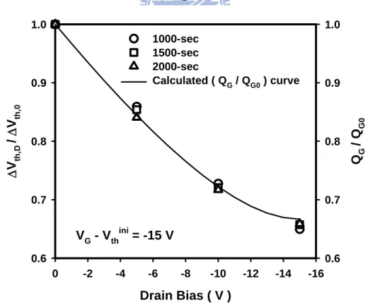
Fig. 3-12. The threshold voltage shift ratio (ΔVth,D/ VΔ th,0) and the normalized channel
charge (QG / QG0) as a function of stressed drain bias……….60
Fig. 3-13. The restored threshold voltage shift as a function of stress time………….60
Fig. 3-14. The linear-region initial transfer characteristic of OTFT……….61
Fig. 3-15. The linear-region transfer characteristics of OTFTs before and after 2000-sec gate bias stress……….61
Fig. 3-16. The shift of mobility and the shift of subthreshold slopes as a function of stress time during gate bias stress……….62
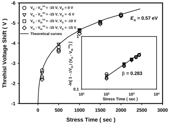
Fig. 3-17. The threshold voltage shift as a function of stress time……….63
Fig. 3-18. The cross-section of pentacene-based TFTs……….63
Fig. 3-19. The scheme of pulse bias function……….64
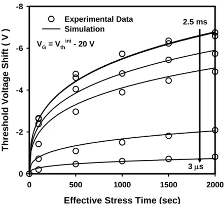
Fig. 3-20. The threshold voltage shift curves are plotted as a function of effective stress time……….64
Fig. 3-21. The equivalent circuit of pentacene-based TFTs……….65
Fig. 3-22. The ΔVth ratio (ΔVthAC-/ΔVthDC-) as a function of pulse width……….65
Fig. 3-23. The calculated curves obtained from Eq.(4) and the experimental data…66 Fig. 3-24. The waveforms of pulsed bias……….66
Fig. 3-25. ΔVth curves with effective stress times are plotted as a function of base voltage duration……….67
Fig. 3-26. The ΔVth plotted as a function of recovery time when VG = 0, 3, 6 V during recovery……….67
Fig. 3-27. ΔVth curves under bipolar pulsed bias stress as a function of effective stress time……….68 Fig. 3-28. The threshold voltage shift curves under steady-state gate bias stress and
Fig. 3-29. ΔVth ratio (ΔVth AC+/ΔVth DC+) as a function of pulse width……….69
Fig. 3-30. The illumination system and conventional top-contact bottom-gate pentacene-based TFT……….70
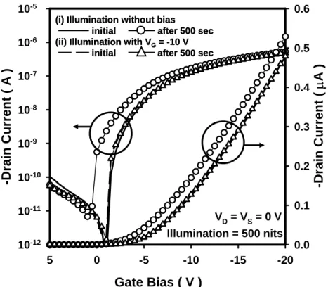
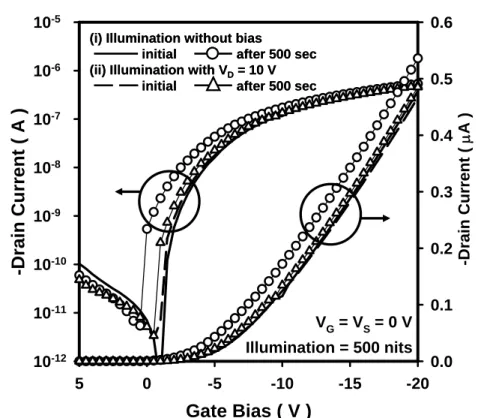
Fig. 3-31. The transfer characteristics of OTFTs before and after a 500-sec illumination with gate bias……….70
Fig. 3-32. Threshold voltage shift and mobility (in the inset) under illumination as a function of negative gate bias……….71
Fig. 3-33. The transfer characteristics of OTFTs before and after a 500-sec illumination with drain bias……….71
Fig. 3-34. Threshold voltage and mobility (in the inset) as a function of positive drain bias……….72
Fig. 3-35. Energy band diagram of organic TFTs from source to drain for 4 cases.………73,74 Fig. 3-36. The light-induced ΔVth as a function of applied bias (Vapp) after a 500-sec illumination……….75
Fig. 3-37. The light-induced ΔVth as a function of recovery time under various drain and source biases……….75
Chapter 4
Fig. 4-1 Molecular structure of PMMA……….91Fig. 4-2 Molecular structure of PVP……….91
Fig. 4-3 Schematic structure of MMF cross-link with PVP……….91
Fig. 4-4 Schematic structure of PVP-OTFTs and PMMA-OTFTs……….92
Fig. 4-5 Wavelength spectrum of light sources (Red, Green, Blue and White).……93
Fig. 4-6 Water contact angle of PVP and PMMA dielectric surfaces………94
Fig. 4-8 The initial transfer characteristic of PVP-OTFT and PMMA-OTFT…….95 Fig. 4-9 X-ray diffraction (XRD) pattern of pentacene deposited on PVP and PMMA dielectrics……….95 Fig. 4-10 Atomic force microscope (AFM) image of (a) PMMA and (b) PVP
dielectric surfaces……….96 Fig. 4-11 Atomic force microscope (AFM) image of pentacene thin film surfaces deposited on (a) PMMA and (b) PVP dielectrics……….96 Fig. 4-12 The linear-region transfer characteristic of PVP-OTFT swept form 15 V to -25 V and back to 15 V in ambient air and under dark……….97 Fig. 4-13 The linear-region transfer characteristic of PMMA-OTFT swept form 10 V to -25 V and back to 10 V in ambient air and under dark………97. Fig. 4-14 The linear-region transfer characteristic of PVP-OTFT swept form 15 V to -25 V and back to 15 V in ambient air and under illumination………….98 Fig. 4-15 The linear-region transfer characteristic of PMMA-OTFT swept form 10 V to -25 V and back to 10 V in ambient air and under illumination……….98 Fig. 4-16 Threshold voltage shift (ΔVth) of PMMA-OTFT and PVP-OTFT after bias
stress under illumination with different wavelength……….99 Fig. 4-17 The absorption spectra of pentacene thin films deposited on PVP and PMMA dielectric……….99 Fig. 4-18 The transfer characteristics of PVP-OTFT and PMMA-OTFT before and
after a 1000-second positive gate bias stress in ambient air and under dark……….100 Fig. 4-19 Fig. 4-19 Threshold voltage shift (ΔVth) of PVP-OTFT and PMMA-OTFT
during positive gate bias stress in ambient air and under dark…………100 Fig. 4-20 The field-effect mobility of both devices plotted as a function of positive bias stress time in ambient air and under dark……….101
Fig. 4-21 The transfer characteristics of PVP-OTFT and PMMA-OTFT before and after a 1000-second negative bias stress in ambient air and under dark……….101 Fig. 4-22 Threshold voltage shifts of PVP-OTFT and PMMA-OTFT during positive gate bias stress in ambient air and under dark………102 Fig. 4-23 The field-effect mobility of both devices plotted as a function of positive
bias stress time in ambient air and under dark………102 Fig. 4-24 Threshold voltage shift of PVP-OTFT and PMMA-OTFT during
illumination……….103 Fig. 4-25 The transfer characteristics of PVP-OTFT and PMMA-OTFT before and
after positive bias stress under illumination………103 Fig. 4-26 Threshold voltage shift (ΔVth) of PVP-OTFT and PMMA-OTFT during
positive gate bias stress under dark and illumination……….104 Fig. 4-27 Energy-band diagram of OTFT from gate to drain/source when devices are under illumination with positive gate bias……….104 Fig. 4-28 Threshold voltage shift of PVP-OTFT during positive gate bias stress under dark and illumination when extending stress time……….105 Fig. 4-29 Threshold voltage shifts of PMMA-OTFT and PVP-OTFT under dark and in air and in vacuum……….105 Fig. 4-30 Threshold voltage shifts of PMMA-OTFT and PVP-OTFT in vacuum under dark and illumination. ………106
Chapter 5
Fig. 5-1 The illumination system and conventional top-contact bottom-gate structure of OTFTs……….118 Fig. 5-2 The initial transfer characteristics of OTFTs with different channel
length……….118 Fig. 5-3 Transfer characteristics of OTFTs before and after a 100-sec illumination
with and without gate bias……….119 Fig. 5-4 The light-induced threshold voltage shifts ΔVthLight as a function of gate
bias……….119 Fig. 5-5 The light-induced threshold voltage shifts ΔVthLight as a function of the
channel length………120 Fig. 5-6 Threshold voltage shift (ΔVth) of PMMA-OTFT during positive gate bias
stress in ambient air when under dark and illumination……….120 Fig. 5-7 Threshold voltage shift (ΔVth) of PMMA-OTFT during positive and
negative gate bias stress in ambient air and under dark……….121 Fig. 5-8 The light-induced ΔVth as a function of recovery time under various gate
biases.………122 Fig. 5-9 Threshold voltage shift of PMMA-OTFT during various bias stresses under dark or during prolonged illumination……….123 Fig. 5-10 Threshold voltage shift of PMMA-OTFT after bias stress under illumination with different light wavelength……….123 Fig. 5-11 Transfer characteristics of OTFT before and after 100-sec illumination with
VG – Vthini = 5 V……….124
Fig. 5-12 Transfer characteristics of OTFT before and after 100-sec illumination with
VG – Vthini = 10 V……….124
Fig. 5-13 Transfer characteristics of OTFT before and after 100-sec illumination with
VG – Vthini = 15 V……….125
Fig. 5-15 ΔVthLight as a function of stress time under various light intensity……….126 Fig. 5-16 Energy-band diagram of OPT from gate to drain/source……….126 Fig. 5-17 Energy-band diagram of OPT from gate to drain/source under illumination with gate bias (15V)……….127 Fig. 5-18 Energy-band diagram of OPT from gate to drain/source under illumination with gate bias (5V)……….127 Fig. 5-19 Energy-band diagram of OPT from gate to drain/source under illumination with gate bias (15V)……….128 Fig. 5-20 Rph as a function of gate stress bias under blue light and white light
illumination……….128 Fig. 5-21 ΔVthLight and photo current difference ΔIph measured by applying periodical
gate bias under various light intensities……….129
Chapter 6
Fig. 6-1 Schematic diagram of the bottom-gate a-Si:H TFT on polyimide substrate……….139 Fig. 6-2 Transfer characteristics of the bottom-gate a-Si:H TFT fabricated at 160°C on polyimide substrate……….139 Fig. 6-3 Output characteristics of the bottom-gate a-Si:H TFT fabricated at 160°C on
polyimide substrate……….140 Fig. 6-4 Transfer characteristics of the bottom-gate a-Si:H TFT before and after
applying 500 sec and 15000 sec gate-bias stress transfer characteristics at 25 °C substrate temperature……….140 Fig. 6-5 Transfer characteristics of the bottom-gate a-Si:H TFT before and after applying 500-sec and 15000-sec gate-bias stress at 60 °C substrate
temperature……….141
Fig. 6-6 ΔVth as a function of stress time at 25°C, 30°C, 40°C, 50°C and 60°C……….141
Fig. 6-7 ΔVth under different stress bias VStress………142
Fig. 6-8 ΔVth as a function of stress bias……….142
Fig. 6-9 ΔVth is plotted as a function of different channel widths……….143
Fig. 6-10 Characteristic temperature (Tch) extraction by fitting the measured ΔVT with those calculated from Eq. (2)……….144
Fig. 6-11 Steps of extracting the channel temperature from the reliability model……….144
Fig. 6-12 Schematic diagram of the a-Si:H TFT thermal equivalent circuit……….145
Fig. 6-13 Extracted Tch as a function of stress bias for devices with channel width………145
Fig. 6-14 Comparison of ΔVth for wide channel device on flat substrate and on bended substrate……….146
Fig. 6-15 Comparison of ΔVth for wide channel device on flat substrate and on bended substrate……….146
Table Caption
Chapter 4
Table 4-1 Spin coating parameters of PMMA and PVP dielectric fabrication process………106
Chapter 1
INTRUDUCTION
1-1 Introduction
In resent years, flexible displays are of great interest especially for mobile applications. Because flexible substrates can not sustain high temperature process temperature, the development of low-temperature process of electronic transistor is necessary. Amorphous silicon (a-Si) and organic materials are promising to fabricate electronics on flexible substrates. The flexible displays have been demonstrated that a-Si thin film transistor (TFT) and organic-based thin film transistor (OTFT) arrays combine with OLEDs, LCDs, and EPDs as shown in Fig. 1-1 (a), (b) and (c) [1-3]. Flexibility can render the display to have new properties such as bendable, rollable, and elastically stretchable. However, lowering temperature process usually affects the stability of electronics. And, the solution process used in OTFT fabrication usually cause residual hydroxyl groups or water molecule in the electrons to lower the lifetime of product.
In this thesis, the reliability issues of OTFTs are studied in steady-state and dynamic operation bias and in different environments. Finally, the self-heating effect of a-Si TFT fabricated on the polyimide substrate is studied.
1-2 Overviews of Organic-Based Thin Film Transistors
Organic thin-film transistors (OTFTs) have received great attention due to their low-cost and large-area array application. In 1960, using small-molecule organic material, condensed hydro-carbons and dyes, successfully fabricated the field effect transistor. However, their semiconductor characteristics were poor and their
reproducibility very low, which caused large difficult to develop any real devices. A relatively minor fundamental interest was maintained in organic materials until the 1970s, when the first world energy crisis launched a renewed interest in organic-based semiconductor, aimed at the development of cheap, flexible, large-area organic-based solar cells. However, after a decade of intense research, both in universities and in private enterprise, results showed that organic semiconductors suffer from severe limitations, linked to the existence of a very high density of defects and traps, as well as to very low carrier mobility. Although significant experimental effort was invested during the 1980s, the inability to increase significantly the carrier mobility above this low value of about 10-4 cm2/Vs led many research groups to question the real potential of organic-based semiconductors for use as active layers in electronic devices. Until 1990s, short conjugated oligmoer and sexithiophene showed the mobility of the order of 10-1 cm2/Vs, almost matching that of a-Si:H TFTs.
To date, the performance of organic thin-film transistors (OTFTs) has been obviously improved by the application of new organic channel compounds and advanced fabrication process. In 2000, field-effect mobility and Ion/Ioff of
pentacene-based TFTs had reached 3.2 cm2V−1s−1 ratio and >109 were demonstrated.
Because the large barrier between Au and pentacene blocks electron injection from contact into the channel, the channel of OTFT is usually P-type. Fig. 1-2 (a) Pentacene is made up of five benzene rings (b) a single pentacene molecule (C22H14)
consists of 5 benzene rings. In each molecule 14 of the 22 C atoms are bonded to two other C atoms and to one hydrogen atom. The four inequivalent H atoms are numbered 1–4. Other H atoms are related by symmetry. (c) A single C22H16 molecule
(dihydropentacene) is shown here. The two C-H2 units are positioned on sites 1 and 8
More recently, displays have been made on OTFT backplanes on flexible polymeric substrates. OTFT arrays to drive liquid crystal (LC) [2] [5] or organic light emitting diode (OLED) [6] which showed full-color moving pictures had been demonstrated. In these reports, OTFTs are encapsulated by passivation layer to avoid exposing to oxygen or moisture in air, and to avoid damage from the subsequent LC or OLED process. When flexible substrates are substituted for conventional glass substrate, the general products can have new application and for different usage as rollable light-weight displays or environmental sensor integrated into clothing or irregular surface of consumer electronics. In particular, organic materials can be deposited at room temperature by spin coating, or by roll-to-roll technology compatible with ink-jet printing. Compared with conventional instruments for fabricating inorganic electric devices, spin coating and roll-to-roll technology can provide low-cost fabrication process due to the lower requirements in vacuum. Because the roll-to-roll technology has high-throughput, the fabrication cost of organic electronic devices on flexible substrates can be further reduced. Here, a roll of thin plastic or metal foil used as the substrate can be kilometers long and meters compared to the glass size of 10 generation about 3 m × 3 m in a flat-panel display (FPD) manufacturing process.
Although the field-effect mobility of organic electric device is already comparable to that of hydrogenated amorphous silicon (a-Si:H), the carrier transport in organic semiconductors, such as pentacene, is sensitive to contamination and is strongly interface-dependent. However, there is difficult to fabricate the very smooth morphology of gate dielectric surface and the uniform of surface state for the large substrate. In the other hand, these organic materials are still sensitive to moisture in ambient air and need superior passivation to cover the organic active layer. Thus, inorganic and organic passivation thin-film technology still has to be further studied.
In previous reports, OTFTs are encapsulated by passivation layer to avoid exposing to oxygen or moisture in air, and to avoid damage from the subsequent LC or OLED process. However, even when devices are encapsulated or operated in an inert environment, OTFTs are known to suffer from bias stress effect (BSE) that causes significant threshold voltage shift.
The bias-stress effect in OTFTs had been studied by using different organic active materials or different gate insulators on different device structures [7]. It was found that, for p-type OTFTs under steady-state bias stress, positive gate bias stress caused a positively-shifted threshold voltage (Vth) and negative gate bias stress caused
a negatively-shifted Vth. The BSE was reversible by removing gate bias or by applying
opposite polarity gate bias. Light irradiation also enhanced the reversal process. However, the prolong illumination causes a positively-shifted Vth. due to trapping
light-induced electrons.
Charge trapping, ion migration, charged-state creation and the formation of bound hole pairs (bipolaron) are several proposed mechanisms to explain the BSE [8]. Charge trapping and ion migration were found to be dominant mechanisms in OTFTs with an organic dielectric [9]. When using thermally-grown SiO2 as the gate dielectric
to study OTFTs reliability, charged-state creation is usually believed to be responsible for the threshold voltage shift (ΔVth). John E. Northrup and Michael L. Chabinyc used
density functional calculation to simulate defect states generation in pentacene film and found that it was due to the formation of oxygen- and hydrogen-related defects such as C-H2, OH, and C-HOH in organic semiconductors [10]. Gu et al. also studied
the response time of the defect states in pentacene. Long-lifetime deep electron traps were proposed to explain the hysteresis effect in pentacene-based OTFTs.
In this thesis, the reliability issues of pentacene-based OTFTs are studied and discussed in the following separated chapters.
1-2-1 Fundamental Transport Mechanism of OTFTs
Band transport mechanism in disordered organic semiconductors dominated by hopping between localized states and carriers are scattered at every step. Hopping is assisted by phonons and mobility increases with temperature, although it is very low overall (μEF << 1 cm2V−1s−1). The boundary between band transport and hopping is
defined by materials having mobilities between 0.1 and 1 cm2V−1s−1 [11, 12, 13]. Highly ordered organic semiconductors, such as several members of the acene series including anthracene and pentacene have room temperature mobilities in this intermediate range, and in some cases temperature-independent mobility has been observed [12], even in polycrystalline thin films of pentacene [13]. That observation was used to argue that a simple temperature-activated hopping mechanism can be excluded as a transport mechanism in high-quality thin films of pentacene [13]. At low temperatures (below approximately 250 K), band transport becomes the mechanism that takes control of carrier transport in single crystals of pentacene and other acenes. Very high mobility values (from 400 cm2V−1s−1 [14] to more than 1000 cm2V−1s−1 [15]) have been reported. At these temperatures, the vibrational energy is much lower than the intermolecular bonding energy and phonon scattering is very low; thus, high mobility is exhibited. At or close to room temperature, phonon scattering becomes so high that the contribution of the band mechanism to transport becomes too small. At these same temperatures, hopping begins to contribute to carrier transport. Hopping of carriers from site to site becomes easier as the temperature rises. The combination of these two mechanisms explains the fact that the mobility decreases as temperature rises from a few degrees K to about 250 K, and after that the mobility begins to rise slowly [14].
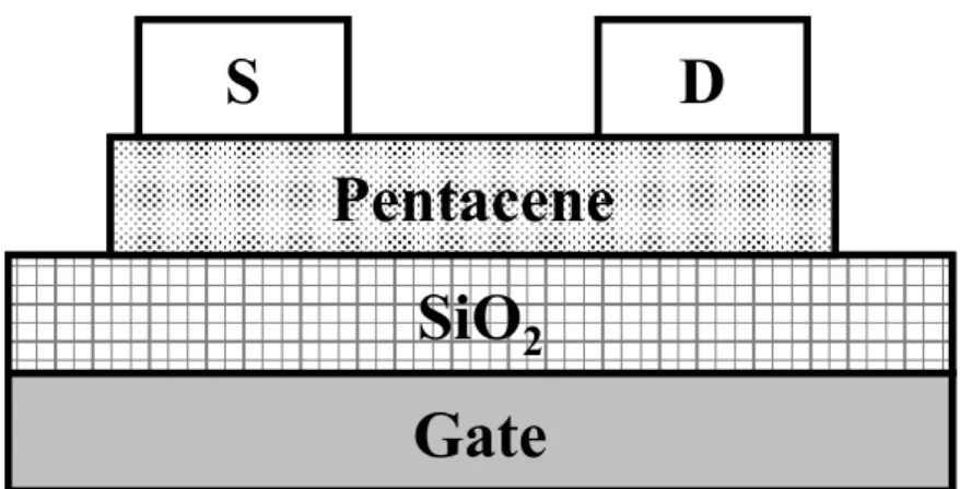
A thin film transistor is composed of three basic elements: (1) a thin semiconductor film; (2) an insulating layer; and (3) three electrodes (source, drain and gate). Fig.1-3 show two kinds of standard OTFT device structure Fig. 1-3(a) is the top-contact device and Fig. 1-3(b) is the bottom-contact device, respectively. The general operation concepts are originated from MOSFET theory. But there is a slight difference, traditional MOSFET are usually operated in inversion mode while the OTFTs are generally operating in accumulation mode. Since the pentacene thin film is a p-type semiconductor due to the characteristic of Au/pentacene contact barrier, the pentacene-based channel is turned on when negative gate bias is applied. The bias-drop across gate dielectric causes the downward energy band bending in the pentacene film near the gate electrode and additional positive charge carriers will accumulate at the interfaces. The gate dielectric is served as a capacitance and can store charges. Applying a drain bias causes a voltage potential difference in the channel and drives the accumulated free carriers to form the drain current.
As shown in Fig. 1-4, the LUMO level of pentacene is quite far away from the Fermi level of gold, so there is a substantial energy barrier for electrons and electron injection is very unlikely. Accordingly, no current passes through the pentacene layer. in contrast, when the gate voltage is reversed to negative, holes are easily injected because the Fermi level is close to the HOMO level and the barrier is low. a conducting channel forms at insulator-semiconductor interface and charge-carriers can be driven from source to drain by applying a second, independent, bias to the drain. Because holes are more easily injected than electrons, pentacene is said to be p-type. Symmetrically, an organic semiconductor is said to be n-type when electron injection is easier than hole injection, which occurs when the LUMO is closer to the Fermi level than the HOMO.
field-effect mobility (μEF), threshold voltage (Vth) and subthreshold slope (S.S.) are
usually served as metric units.
Field-Effect Mobility (μEF):
The μEF can be extracted from the device drain current by using the general
MOSFET drain-current equation. In linear region (VGS – Vth > VDS):
(
)
μ ⎡⎢ ⎤⎥ ⎣ ⎦ 2 DS DS FE ox GS th DS V W I = C V V V -L 2 (1-1)when VDS is small (VGS – Vth >> VDS), Eq. (1-1) can be reduced to
(
)
DS FE ox GS th DS W I = μ C V -V V L (1-2) In saturation region (VGS – Vth < VDS)(
)
μFE ox 2 DS GS th C W I = V -V L 2 (1-3)where Vth, W, L and Cox are the threshold voltage, the channel width, the channel
length and the gate dielectric capacitance per unit area. In linear region, mobility is defined as
∂ ∂ DS FE, linear ox DS GS I L μ = WC V V (1-4)
In saturation region, mobility is defined as 2 DS FE, sat ox GS I 2L = WC V μ ⎡⎢∂ ⎤⎥ ∂ ⎢ ⎥ ⎣ ⎦ (1-5) The field-effect mobility (μEF) is distinct from the more physically fundamental
carrier mobility (μ), which has the same units but relates average carrier velocity v to
applied electric field E. The field-effect mobility (μEF) is easily affected by additional
effects such as parasitic resistant, carrier scattering and current crowding. However, the field-effect mobility (μEF) can be immediately and simply extracted from the
Therefore, using μEF as metric unit is convenient than extracting (μ).
Threshold Voltage (Vth):
The threshold voltage can be extracted from the transfer characteristic in the linear region by plotting IDS versus VGS for small drain voltages (VGS – Vth > VDS), and
extrapolating the line to IDS =0. Fig. 1-5 shows the transfer characteristic in the linear
region. Similarly, the threshold voltage can be extracted from measurements in the saturation region by plotting IDS versus VGS and extrapolating to IDS =0.
Threshold voltage of pentacene-based TFTs is usually large and uncontrolled, and values as high as tens of volts. Until now, the large Vth can not be clearly
explained. However, it is believed that the high density of trapped charge consists at the interface between pentacene film and gate dielectric. For electronic applications, a large threshold voltage causes the power waste and needs larger drive bias to lead to the bias stress effect. To date, some groups successfully use self-assembled monolayer to modify or lower the defect density on the dielectric surface and obtain lower Vth.
Using higher dielectric constant material as gate insulator also can reduce the threshold voltage.
Subthreshold Slope (S.S.):
Based on the simplified physical models underlying Eq. 1-1 and 1-3, the drain current is zero when applied gate bias (VGS) is smaller than threshold voltage (Vth).
Actually, these two equations can not correctly represent the drain current in the subthreshold region. When device is switched from off-state to on-state in the subthreshold region, the power-law dependence between the drain current increase and the gate bias is found. The general current equation in the subthreshold region can be expressed as:
μ ⎛⎜ ⎞⎟ ⎝ ⎠ DS GS -qV qV kT nkT DS FE ox W I = K C 1-e e L (1-6)
Fig. 1-6 shows that the subthreshold region of the transfer characteristic and a straight line through the subthreshold region. The slop of a straight line is relative to the interface state between pentacene film and gate dielectric. Therefore, the inverse of the subthreshold slope usually represents the behavior of subthreshold region. The inverse of the subthreshold slope also is named as the subthreshold swing and expressed as ⎛∂ ⎞ ⎜ ∂ ⎟ ⎝ ⎠ -1 DS GS logI S.S. = V
where the units used for subthreshold slope (S.S.) are volts/decade that represents the
increment in gate voltage needed to change the drain current by a factor of 10.
1-2-3 Hysteresis of OTFTs
Hysteresis, or memory effects is often observed in the transfer characteristics of organic-based TFTs. Hysteresis refers to short-term reversible shifts that lead to looping in the measured characteristics, depending on which direction the bias voltages are swept in. There are usually three mechanisms to explain the hysteresis in p-type organic-based TFT: (1) slow polarization of the gate dielectric, (2) charge storage in the dielectric, and (3) electron trapping in the semiconductor. (1) and (2) mechanisms are dominated by the gate dielectric quality. Mechanism (1) describes that when dipolar groups or molecules consists in a polymer gate dielectric, applied gate electric field cause slow reorientation in dipolar groups or molecule. In this case, hole carriers can not be immediately accumulated in the channel after changing gate bias. The slow accumulation rate leads to hysteresis in the transfer curves. If mechanism (2) dominates the hysteresis, the loop direction can be clockwise and
anticlockwise depending on the sign and location of the injected and stored charge. Therefore, using the loop direction is difficult to differentiate between mechanism (1) and (2). However, when the injected and stored charge existed in the gate dielectric, the gate leakage current is usually affected and the abnormal gate leakage current can represent the mechanism (2). When organic thin film is deposited on the thermally grown silicon dioxide (SiO2) gate dielectric, mechanism (1) and (2) can be excluded
to lead to hysteresis. The hysteresis is induced by trapping electrons in the organic thin film. The electron trap states in the semiconductor are quickly filled and slowly released. When sweeping gate bias from positive to negative bias, initial positive gate bias attracts electron accumulated in the channel and the electron traps are filled. Then, when changing positive gate bias to negative, from off to on, hole carriers are accumulated in the channel and trapped electrons with slow release rate induce extra holes. Extra hole carriers lead to extra drain current during the off-to-on sweep. If changing gate bias sweep direction, on-to-off, there are no trapped electrons to cause extra hole carriers. Therefore, the field-effect mobility (μEF) and threshold voltage (Vth)
are dependent on the direction of sweeping gate bias.
1-2-4 Threshold Voltage Shift Mechanism of OTFTs
The ΔVth of OTFTs is believed due to the carrier trapping by the defect states.
However, there are only a few explanations on the micro process of the defect creation, which can be observed in bias stress experiment. Bias tress experiment can be divided into two kinds: negative bias stress and positive bias stress.
Firstly, micro process of defect creation under negative bias stress is introduced. The formation of bipolaron proposed by R. A. Street et al. [8] is one of the plausible mechanisms. The deep states slowly trap holes to form bipolarons. The formation of bipolarons would cause the ΔVth due to the reduction of mobile holes. The reaction
can be expressed as: BP
h h+ →( hh )
The other possible mechanism was proposed by John John E. Northrup et al. [10] They studied the formation of hydrogen- and oxygen-related defects (C-H2, OH, and
C-HOH) in pentacene film based on the density functional calculation. The defect creation reactions were given as follows:
+ + + + →2( ) 2h C22H16 C22H14 C22H15 and 22 16 22 14 22 15 22 15 2h++C H O C H+ →(C H O)++(C H )+
When the pentacene film is in a hole-rich environment, both these two reactions tend react to the right-hand side and produce positive-charged states that cause ΔVth.
Either bipolaron formation or hydrogen-, oxygen-related defect creation, these studies need more experimental results to support their theories. Both mechanisms assume that the reaction rate is proportional to the carrier concentration.
However, compare with negative bias stress effect, there are fewer studies focused on positive bias stress effect. Applying a prolonged positive bias to the device usually causes electrons trapping in the channel and a threshold voltage shift forward positive bias. After removing the negative bias, the recovery of trapped electrons can be observed and the device threshold voltage comes back to the original value. Until now, the micro process of electron trap generation under the positive bias stress is not discussed in detail.
The reversible positive ΔVth not only caused by positive bias stress but also can
be induced by H2O and O2 in ambient air. When there are lots of OH groups on the
SiO2 surface, SiOH is generated. H2O and O2 are easily absorbed by SiOH to cause
shown as chemical reaction: 2 3 SiOH H O+ ⇔ SiO−+H O+ and O H SiO O e iOH 2 2 2 1 4 1 S + −+ → −+
We can see H2O and O2 contained in air promote the reaction to the right-hand
side and produce negative-charged states that cause the ΔVth. Therefore, if we perform
the measure in vacuum or eliminating OH groups on the dielectric surface, the prolonged positive bias influence on device Vth may be drastically reduced.
1-2-5 Originals of Trapped Carriers
In the above section, the most of reliability studies focus on the defect generation and a few studies discuss the original of trapped carriers. The efficiency of injection of carriers from the metal contact into the HOMO or LUMO of the pentacene thin film depends on the energy barrier φB that carrier has to overcome at the metal/organic semiconductor interface. At the metal/organic semiconductor interface,
φB,e and φB,h depend, respectively, on the position of the LUMO and HOMO relative to the Fermi level of the metal. Fig. 1-7 shows that the Energy-band diagrams of pentacene-based thin film transistor with Au contact metal. Obviously, the work function of Au contact is near the HOMO of pentacene film, The φB,h is smaller than
φB,e. Therefore, the hole carriers are main transport carriers. For originals of trapped hole carriers in the device channel, it is believed that the hole carrier injection from contact is the main mechanism. Because the large φB,e seriously lower the efficiency of electron injection, the electron injection is excluded to provide free electrons in the channel. To date, originals of trapped electrons are fully understood and observed
phenomena can not be satisfactorily explained. There are two plausible mechanisms to explain originals of trapped electrons: (1) light-induced electron traps and (2) hydroxyl groups induced electron traps.
(1) Light-induced electron traps:
When irradiating the device, photons enter the pentacene film to generate the excitions. Then, light-induced excitons dissociate into hole-electron pairs. Some papers report that the dissociation process of light-induced excitons can be enhanced under electric field. High vertical field (higher than 2×10⁴ V/cm [16]) may be
effective in dissociating excitons.
(2) Hydroxyl groups induced electron traps
Based on the above Sec. 1-2-3, the generation process of electron traps has been explained. Hydroxyl groups on gate dielectric or in pentacene film combine with moisture in air to generate electron traps. The originals of hydroxyl groups may come from fabrication process that causes residual hydroxyl groups due to incomplete cross-linking or incomplete baking.
In following chapter 4, the influences of light-induced electrons and hydroxyl groups on gate dielectric are studied and discussed.
1-2-6 Gate Dielectric Surface Treatment
The transfer characteristic of organic-based TFTs strongly depends on the gate dielectric states. There are usually high density of traps consisted on the gate dielectric surface to lower the field-effect mobility, cause the hysteresis and increase the leakage current. Therefore, it is proposed that using various kinds of organic compound treats gate dielectric surfaces of organic-based TFTs to improve the transistor performance. For the first time, Lin et. al. demonstrated that using OTS to treat the dielectric surface improve the mobility of pentacene-based TFTs due to the
lower density of trap states at the interface between the semiconductor and the gate dielectric [17]. To date, many chemical compounds have been used for the surface treatment of gate dielectrics. These chemical compounds are classified into (1) trichlorosilane [18], (2) alkoxysilane [19], (3) phosphonic acid [20] and (4) silazane [21] according to the reaction group. The surface treatment can improve the mobility, threshold voltage and subthreshold slope.
1-3 Overviews of a-Si:H TFTs on Flexible Substrate
Electronic devices fabricated on flexible substrates have been attracted great attention and expected to realize electric books. The advantages of the electric book are portable, low-power, and inexpensive electronics even including wireless. Furthermore, the fabrication cost of a-Si:H TFTs on flexible substrates can be lowered compared to conventional technology due to substrate cost. The cost of glass substrate is usually higher than the polyimide substrate. Therefore, the fabrication cost in a-Si:H TFTs can be lowered and power consumption also can be reduced when process temperature is lower. Although organic based TFTs are attractive due to room-temperature and large-area fabrication process compatibility, these organic materials easily degrade in air and the superior encapsulation are necessary. Furthermore, the transfer characteristic of organic based TFT is very sensitive to the surface states of gate dielectric. The very smooth surface of substrate or gate dielectric is basic requirements to fabricate the uniform characteristic of devices on the large or long substrates.
In the other hand, in order to obtain stable and superior characteristic, process temperature of a-Si:H TFTs is usually higher than 150 oC. However, many polyimide substrates can sustain the temperature varied from 150 oC to 200 oC and the cost is still kept at low. More recently, there have been reports of TFT fabrication at 150◦C
on Kapton E and at 110◦C on polyethylene terephthalate (PET), showing performance characteristics close to those fabricated at 250–300◦C. The gate dielectrics in a-Si:H TFTs and passivation dielectrics are usually based on plasma deposited amorphous silicon nitride (a-SiNx). The basic requirements of a good gate dielectric have to
sustain electric fields of about 2 MV/cm without breakdown and low charge-trapping rate at lower electric fields. When PECVD a-SiNx gate dielectric fabricated at 150oC
for compatibility with flexible plastic substrates, a-SiNx thin film usually have high
hydrogen concentration, poor dielectric performance and the high leakage current. The fabrication process follow is shown in below:
1-3-1 Reliability Issues of a-Si:H TFTs
on plastic substrates
Compared with crystalline silicon transistors, a-Si:H TFTs exhibit threshold voltage shift (ΔVth) under bias stress that causes the drain current to decrease with
time. There are two main mechanisms are responsible for the device ΔVth: (1) the
creation of dangling bonds in a-Si:H film and (2) charge trapped inside the dielectric layer (silicon nitride). In that case (1), the device ΔVth is temperature- and
bias-dependent and irreversible after stress removal. When the ΔVth is induced by
charge trapped, the ΔVth is independent on temperature and dielectric-trapped charges
emitted from defective gate dielectric to a-Si:H layer increase gate leakage current. When decreasing deposition temperature down to the highest working temperature of low-cost polyimide substrate, this low process temperature leads to poorer electronic properties in a-Si:H and in higher charge-trapping rate in the gate dielectric. It was reported that in a-Si:H TFTs fabricated at the substrate temperature of 110 oC, a-Si:H defect generation increased fivefold, whereas the charge trapping in the nitride gate dielectric went up by one order of magnitude.
TFTs is attributed state creation in the a-Si:H thin film. After prolonged bias stress, the ΔVth of a-Si:H TFT is obvious while the field effect mobility and subthreshold
slope remain unchanged. When reaching adequate stress bias, defect state creation in a-Si:H TFTs is no longer dominant and the ΔVth is controlled primarily by charge
injection from the channel into the gate dielectric interface. In our experiment, when process temperature is kept at 160 oC, the device ΔVth is strongly dependent on the
substrate temperature. It means that the SiNx thin film is more stable than thin film at
low process temperature and state creation mechanism is the major mechanism. ΔVth
as a function of stressed gate bias and stress time can be expressed by the stretched-exponential equation [22]: ( ) 1 exp β τ ⎧ ⎡ ⎛ ⎞ ⎤⎫ ⎪ ⎢ ⎥⎪ − = Δ = − ⎨ − −⎜ ⎟ ⎬ ⎢ ⎝ ⎠ ⎥ ⎪ ⎣ ⎦⎪ ⎩ ⎭ ini ini th th th G th t t V V V V V (1-7)
where Vthini is the initial threshold voltage. β is a weakly temperature-dependent
dispersion parameter. τt can be expressed as t 1exp A
E kT
τ ν= − ⎛ ⎞
⎜ ⎟
⎝ ⎠, where ν is an attempt to escape frequency and EA is the mean activation energy for the defect generation.
1-3-2 Self-Heating Effect
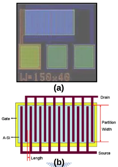
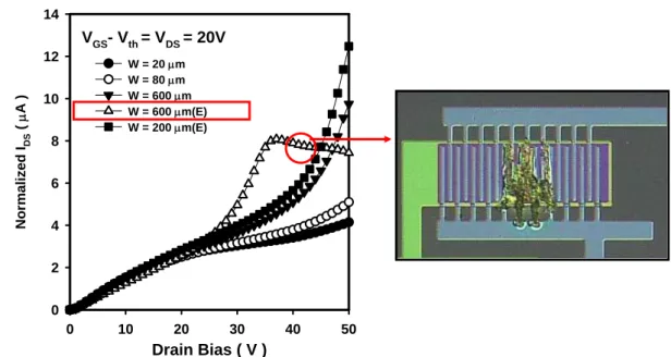
Recently, gate driver circuits of TFT-LCD panel have been successfully fabricated by using conventional a-Si:H TFTs on glass substrates [23]-[25]. The a-Si:H based circuits can lower the amount of driver ICs and simplify the IC bonding process. Because a-Si:H TFTs exhibit low field effect mobility, the enormous channel width such as using the finger structure as shown in Fig. 1-8 or increasing drain bias are usually designed to provide adequate current to drive the pixel array. However, a-Si:H TFTs have the serious reliability issues compared with poly-Si TFTs. The instability of threshold voltage easily causes the fail on the function of circuits.
Unfortunately, in recent studies, it is found that the enormous channel width and large drain bias enhance the ΔVth and cause the damage in the channel by burning. Fig. 1-8
(a) shows that increasing channel width increases the normalized device current and serious degradation generated in a-Si:H TFT with large channel width when reaching adequate operation bias. Fig. 1-9 (b) shows that large current cause damage in the channel by burning [26]. Based on the state creation mechanism; the ΔVth is
proportional to the carrier concentration in the channel. The threshold voltage shift should be independent on the channel width and increasing drain bias can lower the
ΔVth, when gate bias stress is applied. The abnormal ΔVth is attributed to the
self-heating effect. According to the study on self-heating effect in a-Si:H TFTs reported by Wang et al. [27], heat dissipation to the ambient are primarily through the gate, the source and the drain contacts. The path through the gate contact via the gate insulator is the most effective. When heat dissipates through gate contact, the thermal resistance of the substrate dominates the thermal dissipation from gate contact to the ambient. The temperature of device can be estimated by the power consumption equation and the thermal resistance of the substrate. Although the device temperature can be estimated, the accurate device temperature and critical operation bias induced the self-heating effect are still difficult to predicted due to complicated thermal dispersive routes. For example, the gate metal pattern also can affect the self-heating effect. Fig. 1-10 shows the surface temperature distribution of a-Si:H TFT when operated at different bias conditions [26].
1-4 Comparisons between Organic TFTs and a-Si:H TFTs
For the development of devices on flexible substrates, organic TFTs have several advantages compared with a-Si:H TFT :
advantage.
2. Because of the high processing temperature used in a-Si:H thin film deposition, a few of the flexible substrate materials are suitable and these materials are usually expensive. However, the processing temperature of organic TFTs can be lowered to room temperature and are compatible with transparent flexible substrates.
3. Using low-cost processes such as roll-to-roll to manufacture organic TFTs on a large area substrate can significantly reduce cost.
Although the performance of organic TFTs is already better than that of a-Si:H TFT, some drawbacks are still waited for solving :
1. Organic materials are very sensitive to the surface state of gate dielectric. Therefore, for industrial manufacture, the uniformity of OTFTs is a serious issue.
2. These organic materials easily degrade in air and the superior encapsulation technology is needed.
Therefore, there are many groups still use the existing a-Si:H TFT process to develop the device on flexible substrates and have some advantages :
1. For display corporations, the device can be manufactured by using the original instruments.
(a)
(a)
(b)
(c)
(c)
Fig. 1-1 (a) Pentacene-based array combined with light emitting diode [Sony, 2007] (b) Pentacene-based array combined with liquid crystal [Hitachi, Ltd., 2006] (c) Pentacene-based array combined with electrophoresis [National Academy of Sciences, 2001].
(a)
(b)
(c)
(a)
(b)
(c)
Fig. 1-2 (a) Pentacene is made up of five benzene rings (b) a single pentacene molecule (C22H14) consists of 5 benzene rings. In each molecule 14 of the 22 C
atoms are bonded to two other C atoms and to one hydrogen atom. The four inequivalent H atoms are numbered 1–4. Other H atoms are related by symmetry. (c) A single C22H16 molecule (dihydropentacene) is shown here. The two C-H2
Gate
Insulator
Semiconductor
S
D
Gate
Insulator
Semiconductor
S
D
(a)
(b)
Gate
Insulator
Semiconductor
S
D
Gate
Insulator
Semiconductor
S
D
Gate
Insulator
Semiconductor
S
D
Gate
Insulator
Semiconductor
S
D
(a)
(b)
Fig. 1-3 OTFT device configurations: (a) Top-contact device, with source and drain electrodes evaporated onto the organic semiconducting layer. (b) Bottom-contact device, with the organic semiconductor deposited onto the gate insulator and the previously fabricated source and drain electrodes.
Au HOMO LUMO EF 2 3 4 5 6 energy (eV) Au HOMO LUMO EF 2 3 4 5 6 energy (eV)
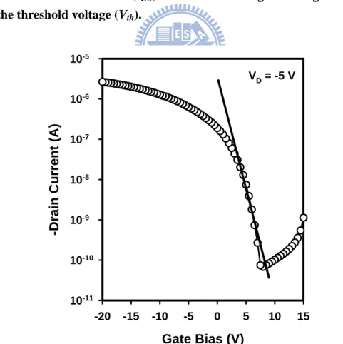
IDS - VGS Gate Bias ( V ) -40 -35 -30 -25 -20 -15 -10 -5 0 5 Drain Current ( μA ) 0.0 0.5 1.0 1.5 2.0 2.5 3.0 3.5
Initial transfer characteristic VD = -5 V Vth Under illumination IDS - VGS Gate Bias ( V ) -40 -35 -30 -25 -20 -15 -10 -5 0 5 Drain Current ( μA ) 0.0 0.5 1.0 1.5 2.0 2.5 3.0 3.5
Initial transfer characteristic VD = -5 V
Vth
Under illumination
Fig. 1-5 Plot of drain current (IDS) as a function of gate voltage for OTFT to
obtain the threshold voltage (Vth).
Gate Bias (V) -20 -15 -10 -5 0 5 10 15 -Drain Curren t (A) 10-11 10-10 10-9 10-8 10-7 10-6 10-5 VD = -5 V Gate Bias (V) -20 -15 -10 -5 0 5 10 15 -Drain Curren t (A) 10-11 10-10 10-9 10-8 10-7 10-6 10-5 VD = -5 V
Fig. 1-6 OTFT transfer characteristics and fitting used for extraction of the subthreshold slope.
Pentacene Au Insulator ELUMO EHOMO B,e
φ
B,hφ
Mφ
Evac(O) Evac(M) Pentacene Au Insulator ELUMO EHOMO B,eφ
B,hφ
Mφ
Evac(O) Evac(M)Fig. 1-7 Schematic of an organic-metal interface energy diagram. φB,e and φB,h are the electron and hole barriers and Evac(O) and Evac(M) are the organic and
(a)
(b)
(a)
(b)
Fig. 1-8 (a) Top view and (b) Schematic diagram of the partitioned a-Si:H TFT named as finger structure.
VGS- Vth = VDS = 20V Drain Bias ( V ) 0 10 20 30 40 50 N o rm aliz ed I DS ( μA ) 0 2 4 6 8 10 12 14 W = 20 μm W = 80 μm W = 600 μm W = 600 μm(E) W = 200 μm(E)
Fig. 1-9 (a) shows that increasing channel width increases the normalized device current and serious degradation generated in a-Si:H TFT with 600 μm when reaching adequate operation bias. (b) large current causes damage in the channel by burning.
Fig. 1-10 The surface temperature distributions of a-Si:H TFT when devices are applied different operation bias [21].