1152 IEEE ELECTRON DEVICE LETTERS, VOL. 30, NO. 11, NOVEMBER 2009
Improved Light Output Power of GaN-Based
Light-Emitting Diodes Using Double Photonic
Quasi-Crystal Patterns
Hung-Wen Huang, Chung-Hsiang Lin, Zhi-Kai Huang, Kang-Yuan Lee, Chang-Chin Yu, and Hao-Chung Kuo
Abstract—The enhancement of light extraction from GaN-based light-emitting diodes (LEDs) with a double 12-fold photonic quasi-crystal (PQC) structure using nanoimprint lithography is presented. At a driving current of 20 mA on a transistor-outline-can package, the light output power of an LED with a nanohole patterned sapphire substrate (NHPSS) and an LED with a double PQC structure are enhanced by 34% and 61%, compared with the conventional LED. In addition, the higher output power of the LED with the double PQC structure is due to better reflectance on NHPSS and higher scattering effect on p-GaN surface using a 12-fold PQC structure pattern. These results provide promis-ing potential to increase the output powers of commercial light-emitting devices.
Index Terms—Gallium nitride (GaN), light-emitting diodes (LEDs), nanoimprint lithography (NIL), photonic quasi-crystal (PQC).
I. INTRODUCTION
T
HE IMPRESSIVE recent developments of high-brightness gallium nitride (GaN)-based light-emitting diodes (LEDs) have made their use in large-size flat-panel displays possible [1], [2]. However, there is still a great need to improve the internal quantum efficiency and external quantum efficiency (EQE) in order to increase the light output power and thus reduce the total cost of LED modules. Research into improving the light extraction efficiency and brightness in LEDs [3]–[8] has been intense. In addition, high-quality GaN-based LEDs are affixed onto a microscale patterned sapphire substrate (PSS) [7], [8]. The microscale patterns serve as a template for the epitaxial lateral overgrowth of GaN and the scattering centers for the guided light. Both the epitaxial crystal quality and light extraction efficiency are improved by utilizing a microscale PSS. Figure [9]–[11] shows the metal–organic chemical vapor deposition (MOCVD) growth of InGaN/GaN LEDs on the PSSs with nanoscale patterns. TheManuscript received April 25, 2009. First published October 6, 2009; current version published October 23, 2009. The review of this letter was arranged by Editor P. K.-L. Yu.
H.-W. Huang is with the Institute of Electro-Optical Engineering, National Chiao Tung University, Hsinchu 300, Taiwan, and also with Luxtaltek Corpo-ration, Miaoli 350, Taiwan (e-mail: [email protected]).
C.-H. Lin, K.-Y. Lee, and C.-C. Yu are with Luxtaltek Corporation, Miaoli 350, Taiwan (e-mail: [email protected]; [email protected]).
Z.-K. Huang and H.-C. Kuo are with the Institute of Electro-Optical En-gineering, National Chiao Tung University, Hsinchu 300, Taiwan (e-mail: [email protected]).
Color versions of one or more of the figures in this letter are available online at http://ieeexplore.ieee.org.
Digital Object Identifier 10.1109/LED.2009.2029985
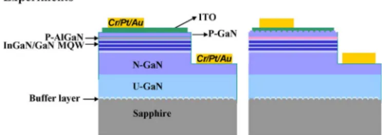
Fig. 1. Schematic diagrams of (a) LED with NHPSS and (b) LED with double PQC structure.
LEDs grown on the nanoscale PSS show greater enhancement in EQE than those grown without nanoscale PSS. To fabricate a nanoscale pattern, e-beam lithography (EBL) [12], laser interference lithography (LIL) [13], self-assembled clusters (SACs) [9], [11], and nanoimprint lithography (NIL) [14], [15] have been used. However, EBL, LIL, and SAC techniques have low throughput and cannot be applied for the mass production of LED devices.
Compared with EBL, LIL, and SAC, NIL is one of the most promising technologies for nanoscale pattern fabrication due to its high resolution and high throughput patterning capability with an extremely low cost for LED devices [15]. In this letter, we utilize a nanoimprinting technique to fabricate a nanohole PSS (NHPSS) and photonic quasi-crystal (PQC) on p-GaN surface to be used for mass production. As a result, the light output efficiency of LED with double PQC pattern is significantly higher than that of a conventional LED.
II. EXPERIMENTS
Fig. 1(a) and (b) shows the schematic diagrams of LED with NHPSS and LED with double PQC structure pattern. In our study, two types are fabricated in order to investigate the influence the NHPSS and double PQC structure has on the LED output power and beam profile performance. In Fig. 1(a), the LED structure consists of a Cr/Pt/Au p-electrode, an indium tin oxide (ITO) transparent layer, an LED epitaxial layer, a smooth p-GaN surface, and a Cr/Pt/Au n-electrode on NHPSS. Furthermore, the LED structure of Fig. 1(b) differs from that of Fig. 1(a), which is the use of NIL process on p-GaN surface with PQC pattern.
The following details are the process flow of NIL on a sapphire substrate. First, we spin coat a 200-nm polymer layer on the sapphire sample surface. Second, we place a patterned mold onto the dried polymer film. By applying a high pressure,
HUANG et al.: IMPROVED LIGHT OUTPUT POWER OF GaN-BASED LEDs 1153
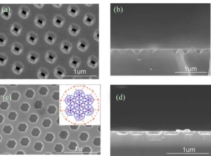
Fig. 2. SEM images of (a) top view of sapphire surface with NHPSS, (b) cross section of sapphire surface with NHPSS, (c) top view of p-GaN surface with PQC (the inset shows the 12-fold PQC structure model), and (d) cross section of p-GaN surface with PQC.
we can heat the LED samples to above the glass transition temperature of the polymer. Third, the LED samples and the mold are cooled down to room temperature to release the mold. Finally, we use an inductively coupled plasma reactive ion etching (RIE) (ICP-RIE) with BCl3/Ar plasma to transfer the pattern onto the sapphire substrate and remove the polymer layer with O2plasma etching gas in a RIE system. Fig. 2(a) and (b) shows both the top and cross-sectional views of scanning electron microscope (SEM) images on a sapphire with NHPSS. The SEM image [Fig. 2(a)] shows the square–triangular lattice of NHPSS with square holes, which is defined by NIL. The lattice constant a of PQC structure is 450 nm, and the hole diameter d (240 nm) is fixed to ratio d/a = 0.53. Fig. 2(b) shows a SEM image of the etching depth and sidewall angle of NHPSS to be approximately 165 nm and 45◦.
All LED samples are grown by MOCVD with a rotating-disk reactor (Veeco) on a c-axis sapphire (0001) substrate at a growth pressure of 200 mbar. The LED structure consists of a 50-nm-thick GaN nucleation layer grown at 500 ◦C, a 2-μm undoped GaN buffer, a 2-μm-thick Si-doped GaN buffer layer grown at 1050◦C, an unintentionally doped InGaN/GaN multiple quantum well (MQW) active region grown at 770◦C, a 50-nm-thick Mg-doped p-AlGaN electron blocking layer grown at 1050◦C, and a 120-nm-thick Mg-doped p-GaN con-tact layer grown at 1050◦C. The MQW active region consists of five periods of 3-nm/20-nm-thick In0.18Ga0.82N/GaN quantum well layers and barrier layers.
Initially, the LED samples with NHPSS are fabricated using the NIL process on p-GaN surface for LED with double PQC structure [in Fig. 1(b)]. Fig. 2(c) and (d) shows a top and cross-sectional view of a SEM with 12-fold PQC pattern based on a square–triangular lattice (inset in Fig. 2(c), right side model). We choose the 12-fold PQC pattern due to the better enhancement of surface emission. This is obtained from the photonic crystals (PCs) with a dodecagonal symmetric quasi-crystal lattice, as opposed to regular PCs with triangular lat-tice and eightfold PQC [16]. The recursive tiling of offspring dodecagons packed with random ensembles of squares and triangles in dilated parent cells forms the lattice. The lattice
Fig. 3. (a) Current–voltage (I–V ) characteristics of conventional LED, LED with NHPSS, and LED with double PQC structure. (b) Intensity–current (L–I) characteristics of conventional LED, LED with NHPSS, and LED with double PQC structure.
constant and hole diameters are 450 and 275 nm, respectively. Fig. 2(d) shows the PQC etching depth of the p-GaN layer to be approximately 80 nm.
In this letter, our LED samples are fabricated using the fol-lowing standard processes with a mesa area of 335× 335 μm2. A SiO2layer with a thickness of 300 nm is deposited onto the LED sample surface by using plasma-enhanced chemical vapor deposition. Photolithography is used to define the mesa pattern after wet etchings of SiO2by a buffered oxide etchant solution. The mesa etching is then performed with Cl2/BCl3/Ar etching gas in an ICP-RIE system in order to transfer the mesa pattern onto an n-GaN layer. A 270-nm-thick ITO layer is subsequently evaporated onto the LED sample surface. The ITO layer has a high electrical conductivity and a high transparency (> 95% at 460 nm). Cr/Pt/Au contact is subsequently deposited onto the exposed n- and p-type GaN layers to serve as the n- and p-type electrodes.
III. RESULTS
Fig. 3(a) shows the characteristics of a typical current– voltage (I–V ). It is found that the measured forward voltages under an injection current 20 mA at room temperature for conventional LED, LED with NHPSS, and LED with double PQC structure are 3.11, 3.08, and 3.12 V, respectively. In ad-dition, the dynamic resistance of conventional LED, LED with NHPSS, and LED with double PQC structure are about 16.0, 16.1, and 16.3 Ω, respectively. Therefore, in terms of dynamic resistance, there is no influence on this type of devices by incorporating NHPSS and PQC structure by the NIL process.
The light output is detected by calibrating an integrating sphere with Si photodiode on the package device, so that the light emitted in all directions from the LED can be collected. The intensity–current (L–I) characteristics of conventional LED, LED with NHPSS, and LED with double PQC structure are shown in Fig. 3(b). At an injection current of 20 mA and a peak wavelength of 455 nm for transistor outline (TO)-can package, the light output powers of conventional LED, LED with NHPSS, and LED with double PQC structure on the TO can are 14.0, 18.7, and 22.5 mW, respectively. Hence, the enhancement percentages of LED with NHPSS and LED with double PQC structure are 34% and 61%, respectively, compared to that of conventional LED. The higher enhancement from standard LED type is due to the effect of the NHPSS, which al-lows the light to reflect from the sapphire substrate onto the top
1154 IEEE ELECTRON DEVICE LETTERS, VOL. 30, NO. 11, NOVEMBER 2009
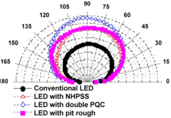
Fig. 4. Far-field pattern of conventional LED, LED with NHPSS, and LED with double PQC structure at a driving current 20 mA.
direction. In addition, the use of a 12-fold PQC pattern results in higher scattering effect and higher epitaxial crystal quality [9]–[11] which increases more light output power. In addition, the corresponding wall plug efficiencies of conventional LED, LED with NHPSS, and LED with double PQC structure are 23%, 30%, and 36%, respectively. This is a substantial improve-ment for the PQC structures as well.
To further study the influence of the PQC structure on the devices, we also measured the light output radiation patterns of the compared LEDs packaged in TO cans at a driving current of 20 mA, as shown in Fig. 4. To compare the aver-age radiation pattern data of LEDs with NHPSS and double PQC structure with that of conventional LED, the radiation pattern data are measured on the 10ea TO-can package de-vices. It can be seen that the LED with NHPSS and LED with double PQC structure possess much higher extraction efficiency with view angles of about 135◦ and 127◦, respec-tively, compared to a view angle of 131◦ for the conven-tional LED. In general, the LED with pit rough surface has a view angle of about 137◦ on the same LED structure. There-fore, the LED with double PQC structure results in a clear view angle variation of ∼10◦ in this experimental 450-nm pitch design. This enhancement is attributed to a broad light beam shaping effect under NHPSS and a narrower beam profile from PQC structure on p-GaN surface in vertical direction using the NIL process.
IV. SUMMARY
GaN-based LEDs with a double 12-fold PQC structure have been fabricated and demonstrated. At a driving current of 20 mA on TO-can package, the light output power of LEDs with the double PQC structure is enhanced by a factor of 1.61. The higher output power of the LED with double PQC is due to higher reflectance on NHPSS and higher scattering effect on p-GaN surface using the 12-fold PQC pattern. This letter offers
promising potential to increase output powers of commercial light-emitting devices.
REFERENCES
[1] M. Koike, N. Shibata, H. Kato, and Y. Takahashi, “Development of high efficiency GaN based multiquantum-well light-emitting diodes and their applications,” IEEE J. Sel. Topics Quantum Electron., vol. 8, no. 2, pp. 271–277, Mar./Apr. 2002.
[2] E. F. Schubert, Light-Emitting Diodes. Cambridge, U.K.: Cambridge Univ. Press, 2003.
[3] S. J. Chang, C. S. Chang, Y. K. Su, C. T. Lee, W. S. Chen, C. F. Shen, Y. P. Hsu, S. C. Shei, and H. M. Lo, “Nitride-based flip-chip ITO LEDs,”
IEEE Trans. Adv. Packag., vol. 28, no. 2, pp. 273–277, May 2005.
[4] J. Song, D. S. Lee, J. S. Kwak, O. H. Nam, Y. Park, and T. Y. Seong, “Low resistance and reflective Mg-doped indium oxide–Ag ohmic contacts for flip-chip light-emitting diodes,” IEEE Photon. Technol. Lett., vol. 16, no. 6, pp. 1450–1452, Jun. 2004.
[5] A. David, T. Fujii, B. Moran, S. Nakamura, S. P. DenBaars, C. Weisbush, and H. Benisty, “Photonic crystal laser lift-off GaN light-emitting diodes,”
Appl. Phys. Lett., vol. 88, no. 13, pp. 133 514-1–133 514-3, Mar. 2006.
[6] J. K. Kim, T. Gessmann, H. Luo, and E. F. Schubert, “GaInN light-emitting diodes with RuO2/SiO2/Ag omni-directional reflector,” Appl.
Phys. Lett., vol. 84, no. 22, pp. 4508–4510, May 2004.
[7] T. S. Oh, S. H. Kim, T. K. Kim, Y. S. Lee, H. Jeong, G. M. Yang, and E. K. Suh, “GaN-based light-emitting diodes on micro-lens patterned sapphire substrate,” Jpn. J. Appl. Phys., vol. 47, no. 7, pp. 5333–5336, 2008.
[8] D. S. Wuu, W. K. Wang, K. S. Wen, S. C. Huang, S. H. Lin, R. H. Horng, Y. S. Yu, and M. H. Pan, “Fabrication of pyramidal patterned sapphire substrates for high-efficiency InGaN-based light emitting diodes,”
J. Electrochem. Soc., vol. 153, no. 8, pp. G765–G770, 2006.
[9] H. Gao, F. Yan, Y. Zhang, J. Li, Y. Zeng, and G. Wang, “Enhancement of the light output power of InGaN/GaN light-emitting diodes grown on pyramidal patterned sapphire substrates in the micro- and nanoscale,”
J. Appl. Phys., vol. 103, no. 1, pp. 014 314-1–014 314-5, Jan. 2008.
[10] J. J. Chen, Y. K. Su, C. L. Lin, S. M. Chen, W. L. Li, and C. C. Kao, “En-hanced output power of GaN-based LEDs with nano-patterned sapphire substrates,” IEEE Photon. Technol. Lett., vol. 20, no. 13, pp. 1193–1195, Jul. 2008.
[11] C. H. Chiu, H. H. Yen, C. L. Chao, Z. Y. Li, P. C. Yu, H. C. Kuo, T. C. Lu, S. C. Wang, K. M. Lau, and S. J. Cheng, “Nanoscale epitaxial lateral overgrowth of GaN-based light-emitting diodes on a SiO2
nanorod-array patterned sapphire template,” Appl. Phys. Lett., vol. 93, no. 8, pp. 081 108-1–081 108-3, Aug. 2008.
[12] C. F. Lai, H. C. Kuo, C. H. Chao, H. T. Hsueh, J. F. T. Wang, W. Y. Yeh, and J. Y. Chi, “Anisotropy of light extraction from two-dimensional photonic crystal light-emitting diodes,” Appl. Phys. Lett., vol. 91, no. 12, pp. 123 117-1–123 117-3, Sep. 2007.
[13] I. B. Divliansky, A. Shishido, I. C. Khoo, T. S. Mayer, D. Pena, S. Nishimura, C. D. Keating, and T. E. Mallouk, “Fabrication of two-dimensional photonic crystals using interference lithography and elec-trodeposition of CdSe,” Appl. Phys. Lett., vol. 79, no. 21, pp. 3392–3394, Nov. 2001.
[14] K. J. Byeon, S. Y. Hwang, and H. Lee, “Fabrication of two-dimensional photonic crystal patterns on GaN-based light-emitting diodes using ther-mally curable monomer-based nanoimprint lithography,” Appl. Phys.
Lett., vol. 91, no. 9, pp. 091 106-1–091 106-3, Aug. 2007.
[15] S. J. Chang, C. F. Shen, W. S. Chen, C. T. Kuo, T. K. Ko, S. C. Shei, and J. K. Sheu, “Nitride-based light emitting diodes with indium tin oxide electrode patterned by imprint lithography,” Appl. Phys. Lett., vol. 91, no. 1, pp. 013 504-1–013 504-3, Jul. 2007.
[16] Z. S. Zhang, B. Zhang, J. Xu, K. Xu, Z. J. Yang, Z. X. Qin, T. J. Yu, and D. P. Yu, “Effects of symmetry of GaN-based two-dimensional pho-tonic crystal with quasicrystal lattices on enhancement of surface light extraction,” Appl. Phys. Lett., vol. 88, no. 17, pp. 171 103-1–171 103-3, Apr. 2006.