國
立
交
通
大
學
電信工程學系碩士班
碩
士
論
文
二維電磁晶體之散射特性分析~實驗驗證
Experimental Study on the Transmittance of Plane Wave by a
Two-Dimensionally Electromagnetic Crystal
研 究 生:黃獻東
指導教授:陳君鍵 博士
黃瑞彬 博士
二維電磁晶體之散射特性分析~實驗驗證
Experimental Study on the Transmittance of Plane Wave by a
Two-Dimensionally Electromagnetic Crystal
研 究 生:黃獻東 Student:Shien-Tung Huang
指導教授:陳君鍵 博士 Advisor: Dr. Kuan-Kin Chan
黃瑞彬 博士
Dr.
Ruey
Bing
Hwang
國 立 交 通 大 學
電 信 工 程 學 系 碩 士 班
碩 士 論 文
A Thesis
Submitted to Department of Communication Engineering College of Electrical Engineering and Computer Science
National Chiao Tung University In partial Fulfillment of the Requirements
For the Degree of Master of Science
in
Electrical Engineering July 9, 2004
二維電磁晶體之散射特性分析~實驗驗證
研究生:黃獻東 指導教授:陳君鍵 博士 黃瑞彬 博士 國立交通大學電信工程學系碩士班 中文摘要 本篇論文中,我們研究了二維電磁晶體之電磁散射特性,此二維電磁晶體由多層 一維金屬線條陣列塗佈於介質材料所堆疊而成。為了量測電磁晶體的穿透特性, 我們使用向量網路分析儀作閉路式量測,同時設計並製作一量測設備,主要包含 兩個寬頻號角天線以及微波光罩來產生一涵蓋有限面積之均勻平面電磁波以入射 該電磁晶體。此外,我們將這些量測設備放置於無反射實驗室以避免外界干擾, 同時亦可消除多重路徑反射之電磁波。經由精密之實驗量測,獲得與經由精確波 模匹配理論計算相當一致之結果,該研究除了證實此量測工作的標準性及一致性 之外,同時亦證明該量測製具之準確性。Experimental Study on the Transmittance of Plane Wave by a
Two-Dimensionally Electromagnetic Crystal
Student: Shien-Tung Huang Advisor: Dr. Kuan-Kin Chan
Dr. Ruey Bing Hwang
Department of Communication Engineering National Chiao-Tung University
Abstract
In this thesis, we have studies the scattering characteristics of a two-dimensional Electromagnetic (EM) crystal made up of metal strips arrays. To measure the transmittance of the EM crystal, we have setup a test fixture containing two wide-band double ridged horns and a microwave mask employed to generate a finite size uniform plane wave for illuminating the EM crystal. Besides, we have put this test fixture in an anechoic chamber to avoid the interference and, meanwhile, to suppress the multiple scattering. We have taken numerous measurements by changing some structural parameters in conjunction with the 2-D EM crystal. The good agreement between those measured data and the theoretical computation based on the program ECMRY [18] prove the standard and consistent measurement in this research work.
Acknowledgement
I would like to acknowledge professor Kuan-Kin Chan, professor Ruey-Bing Hwang. For their guidance and suggestions, this thesis can be accomplished.
CONTENTS
CHINESE ABSTRACT Ⅰ ENGLISH ABSTRACT Ⅱ ACKNOWLEDGMENT Ⅲ CONTENTS Ⅳ FIGURE CAPTIONS Ⅵ CHAPTER 1 INTRODUCTION 1 CHAPTER2 PROBLEM DESCRIPTION 4 2-1 Structural of configuration 4 CHAPTER3CALIBRATION PROCEDURE FOR TRANSMITTANCE MEASUREMENT 6
3-1FRIIS TRANSMISSION EQUATION 6
3-2PROPAGATION LOSS 7
3-3 TEST FIXTURE 7
3-4CALIBRATION PROCEDURE 9
CHAPTER4
EXPERIMENTAL AND NUMERICAL RESULTS 18
4-1SCATTERING CHARACTERISTICS OF A 2-DEM CRYSTAL 18
CHAPTER5
CONCLUSION 37
Figure Captions
Figure 2-1 Structural configuration and geometric parameters for 2-D Electromagnetic crystal 5 Figure 2-2 The realization of the 2-D EM crystal consisting of silver foils and Polystyrene substrate 5
Figure 3-1 Electromagnetic Crystals measurement system 11
Figure 3-2 Gain of double ridged horn antenna 12
Figure 3-3 Gain of wideband power amplifier and insertion loss of coaxial cables 13 Figure 3-4 Beamwidth of radiation gain pattern of the model-0115 double ridged horn antenna 14 Figure 3-5 Transmission efficiency for the two face-to-face horn antennas 15 Figure 3-6 Variation of propagation loss against the frequency; results for measurement and calibration 16 Figure 3-7 Photograph of Electromagnetic crystals measurement system 17 Figure 4-1 Variation of transmittance against frequency for both experimental measurement and
theoretical calculations; z-polarized wave incidence; for two 1-D metal strip arrays having the same metal
width 15 mm, lateral shift 0 mm, separator 24 mm, and metal thickness 0.06 mm 23 Figure 4-2 Variation of transmittance against frequency for both experimental measurement and
theoretical calculations; x-polarized wave incidence; for two 1-D metal strip arrays having the same metal width 15 mm, lateral shift 0 mm, separator 24 mm, and metal thickness 0.06 mm 24 Figure 4-3 Variation of transmittance against frequency for both experimental measurement and
theoretical calculations; z-polarized wave incidence; for two 1-D metal strip arrays having the same metal width 10 mm, lateral shift 0 mm, separator 24 mm, and metal thickness 0.06 mm 25 Figure 4-4 Variation of transmittance against frequency for both experimental measurement and
theoretical calculations; x-polarized wave incidence; for two 1-D metal strip arrays having the same metal width 10 mm, lateral shift 0 mm, separator 24 mm, and metal thickness 0.06 mm 26 Figure 4-5 Variation of transmittance against frequency for both experimental measurement and
theoretical calculations; z-polarized wave incidence; for three 1-D metal strip arrays having the same
metal width 10 mm, lateral shift 0 mm, separator 24 mm, and metal thickness 0.06 mm 27 Figure 4-6 Variation of transmittance against frequency for both experimental measurement and
theoretical calculations; x-polarized wave incidence; for three 1-D metal strip arrays having the same
Figure 4-7 Variation of transmittance against frequency for both experimental measurement and theoretical calculations; z-polarized wave incidence; for four 1-D metal strip arrays having the same
metal width 10 mm, lateral shift 0 mm, separator 24 mm, and metal thickness 0.06 mm 29 Figure 4-8 Variation of transmittance against frequency for both experimental measurement and
theoretical calculations; x-polarized wave incidence; for four 1-D metal strip arrays having the same
metal width 10 mm, lateral shift 0 mm, separator 24 mm, and metal thickness 0.06 mm 30 Figure 4-9 Variation of transmittance against frequency for both experimental measurement and
theoretical calculations; z-polarized wave incidence; for four 1-D metal strip arrays having the same metal width 10 mm, lateral shift 0 mm, and metal thickness 0.06 mm with different separator 24, 48 and
24 mm 31
Figure 4-10 Variation of transmittance against frequency for both experimental measurement and theoretical calculations; x-polarized wave incidence; for four 1-D metal strip arrays having the same metal width 10 mm, lateral shift 0 mm, and metal thickness 0.06 mm with different separator 24, 48 and
24 mm 32
Figure 4-11 Variation of transmittance against frequency for both experimental measurement and theoretical calculations; z-polarized wave incidence; for four 1-D metal strip arrays having the same metal width 10 mm, lateral shift 0 mm, and metal thickness 0.06 mm with different separator 24, 72 and
24 mm 33
Figure 4-12 Variation of transmittance against frequency for both experimental measurement and theoretical calculations; x-polarized wave incidence; for four 1-D metal strip arrays having the same metal width 10 mm, lateral shift 0 mm, and metal thickness 0.06 mm with different separator 24, 72 and
24 mm 34
Figure 4-13Variation of transmittance against frequency for both experimental measurement and theoretical calculations; z-polarized wave incidence; for six 1-D metal strip arrays having the same separator 24 mm, lateral shift 0 mm, and metal thickness 0.06 mm with different metal width 10, 10, 10,
10, 10, 15, and 15 mm 35
Figure 4-14 Variation of transmittance against frequency for both experimental measurement and theoretical calculations; x-polarized wave incidence; for six 1-D metal strip arrays having the same separator 24 mm, lateral shift 0 mm, and metal thickness 0.06 mm with different metal width 10, 10, 10,
Chapter 1: Introduction
Periodic structures have been widely studied in microwave engineering for many years [1-7]. To mention a few, the 1-D (one-dimensionally) periodic dielectric waveguide has been investigated and implemented in the applications of grating coupler in integrated optics [3]; it could also serve as a diffraction grating to diffract the incident beam into a specific direction. However, most of the applications were limited to the 1-D periodic structures. The two and three dimensional ones are seldom tackled in that period. Up to 1970s, the two-dimensionally periodic structures were found to have the capabilities of filtering the incident wave in both the spectral and space domain [8-10]. By suitable designing its periodic pattern of the unit cell, it can allow specific frequency bands to pass through and stop the other ones, so it was named as frequency selective surface. This opens the applications of FSS (Frequency Selective Surface) in microwave antenna applications. Although, in the beginning, they were focused on the military and deep space applications, recently they are employed as the radome incorporated with a feed horn for acting as a high gain antenna in commercial wireless communication network.
After 1996, the two-dimensionally periodic structures, implemented on the microwave substrate by printed circuit technology, were developed to suppress the propagation of surface waves. Such a kind of structures was named as a high impedance surface invented by UCLA groups [11-12]. However, the physical consequences in conjunction with the reason why the compact size (less than half-wavelength) and few unit cells with the structures can achieve the good performance were unknown. In 1999, Hwang and Peng [13] first used the 2-D periodic impedance surface model to successfully account for the guiding characteristics of the surface waves supported by the structures. Besides, they believed that the high impedance surface should belong to the class of resonance type periodic structure. They revisited the corrugated metal surface and rigorously calculated the dispersion relation of the wave guided in the structure [14]. In their theoretical computations, multiple modes are all included and the contributions from higher order modes are clearly identified. The numerical results reveal that the strong dispersion with the unit cell indeed further reduces the starting position of the stop band, and also enhances the attenuation constant of waves in the stop band region. The former two conclusions directly explain the former questions with the UCLA’s high impedance surface.
society for the two and three dimensionally periodic structures, for examples, the arrays having split rings backed with metal strips [15]; the 2-D transmission line network equipped with lumped resonant elements. They were experimentally proved to have the capabilities in lensing the propagation and non-propagation waves [16], as well. Besides, they were shown to be able to focus the incident beam in such a kind of medium, that is, the refraction at the boundary between a conventional and such a kind of medium is abnormal, which contradicts the Snell’s law. Therefore, this medium is named as a left-handed medium to distinguish from the commonly used one. At the same time, many researchers recall a paper published in 1968 by a Russian scientist [17], in that paper he had predicted the wave propagation behavior in a medium simultaneously exhibiting negative permittivity and permeability. In theoretical analysis, he found, in that medium, the wave possesses anti-parallel between the Poynting- and propagation- vector. That is the reason why the wave can be lensed there. As a consequence, many researchers believe the negative permittivity and permeability are the main reasons for the phenomenon of ultra-refraction. Although the refraction anomalous was found, the band with of operation is so narrow, and a strong attenuation is occurring, at the same time. Therefore, the rigorous model for predicting and accounting for the physical mechanism remains to be studied in detail.
From the literatures described previously, we know that the 2-D periodic structure containing metal and dielectric media is the basic one and has not yet studied clearly in the literatures. In 2004, Hwang [18] employed the mode-matching method invoking the general eigen-value method to rigorous resolve the dispersion relation of wave propagation in a metallo-dielectric medium. From now on, I will call it as 2-D EM (electromagnetic) crystal through this thesis. All the higher order modes are considered to figure out the band structure of fundamental modes and higher order modes and their space harmonics, as well. In addition, the relationship between the band structures and the scattering characteristics has also been clearly identified in this paper.
In this thesis, we have employed the experimental way to verify the theoretical computation based on the theory established in that paper. The test fixture containing two wide-band double ridge horns and a microwave mask used to truncate the incident beam into a uniform plane wave of finite aperture was implemented in an anechoic chamber. We have implemented the 2-D EM crystal by using metal strips coated on Polystyrene slabs. To clearly understand the band structure with the crystal, in this thesis, we have changed the structure parameters to identify the frequency band and attenuation of wave in connection
with the stop bands. The excellent agreements between the theoretical and experimental results validate the consistent and standard measurement procedure and a robust text fixture in this research work.
The organization of this thesis is described as follows. The first chapter introduces the basic principle for the measurement equipments including a vector network analyzes, power amplifier, double ridge horn and the other accessory. Besides, the possible errors due to these accessories will also be indicated. The succeeding chapter will discuss the calibration procedure for this experiment. Since the theoretical calculation is on the basis of plane wave incidence, the measured data should be de-embeded to the surfaces of the 2-D EM crystal. The mathematical procedure relating the calibration will be illustrated in this chapter. The ensuing chapter will deal with the measurement of transmittance of plane wave through the 2-D EM crystal. We will systematically demonstrate the results obtained by theoretical and experimental ways and account for the possible physical mechanism involved, in particular for the stop-band behavior. The final chapter will conclude this research work by imposing some remarks.
Chapter 2: Description of the Problem
2-1 Structural of configuration
A two dimensional EM crystal, shown in the figure 2-1, can be regarded as finite stack of one dimensionally periodic structure. As the rectangular coordinate system attached, the infinite metal strip array extends infinitely in z-direction. Each of the metal-strip has width wm and
thickness hm, and the separation between two strips is wa. Thus, the periodic of the metal
strip array in x-direction is dx (wm+wa). It is noted that the metal strip considered in this
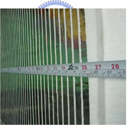
thesis is assumed to be a perfect conductor; namely, there is no electric field distribution in it. However, for the case of metal strip finite conductivity, it should include the contribution of metal modes, which is beyond the scope of this research work, and we will not tackle the problem. The realization of the 2-D EM crystal is shown in figure 2-2.
Returning to figure 2-1, a uniform dielectric layer having relative dielectric constant denoted by εr and thickness s, serves as a separator to separate the 1-D metal strip arrays.
Furthermore, each of the 1-D metal strips array has a distance shift ls in the lateral direction
(x-axis). The lateral shift distance ls determines the pattern of a 2-D EM crystal; for instance,
if the ls for each 1-D metal strip array is set to be zero, a 2-D EM crystal of rectangular pattern
is obtained; if the later shift distances for two adjacent layers are 0.0 and 0.5dx, alternatively, is a triangular pattern. For a rectangular pattern, the period in y-direction can be simply figure out by dy=hm+s. As shown in this figure, a plane wave is obliquely incident into this
structure. The incident angle, θi, is defined as the angle between y-axis and the
propagation vector (inc)
Figure 2-1 Structural configuration and geometric parameters for 2-D Electromagnetic crystal
Figure 2-2 The realization of the 2-D EM crystal consisting of silver foils and Polystyrene substrate
Chapter 3: Calibration procedure for transmittance measurement
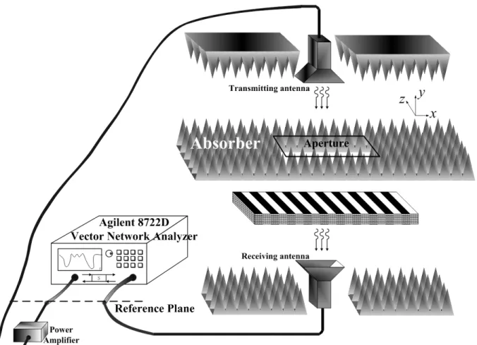
In this chapter, we will present a test fixture for measuring the scattering characteristics of EM crystals by a plane wave normally incident. This measurement system consists of microwave power amplifiers, coaxial cables, board band double ridged horn antennas and anechoic chamber.
Since the measurement of transmission efficiency is defined as the radio of transmitted power to incident power at the input- and output- interface of the EM crystal, respectively, thus, we should calibrate the physical quantities to the two prescribed interfaces. In do so, we should take away the effects due to measurement accessory, such as the antenna factor, cable losses, amplifier gain and propagation loss with the plane wave. The procedure described previously is so called as calibration in microwave measurement.
In this chapter, we will introduce the procedure for calibrating the accessories of measurement to obtain a standard and consistent result for the transmission efficiency measurement with the EM crystals.
3-1 Friis transmission equation
This calibration work is based on the theory of Friis transmission formula written as equation 3-1, it is well known in microwave engineering system and defines the relationship between transmitting and receiving power.
r t t r G G R P P 2 4 ⎟⎠ ⎞ ⎜ ⎝ ⎛ = π λ 3-1 Where
Pt: power transmitted by the transmitting antenna Pr: power received by receiving antenna
Gt: gain of transmitting antenna Gr: gain of receiving antenna
λ: operation wavelength
The equation shown in equation 3-1 is valid for wave propagation in free space. However, the term 2 4 ⎟⎠ ⎞ ⎜ ⎝ ⎛ R π λ
chary to as the propagation environment varies. In this research, we employ the anechoic chamber to mimic the environment of free space, such that the equation 3-1 works.
3-2 Propagation loss
Equation 3-1 illustrates the relationship between transmitted and received power at the two horn antennas. However, what we want to understand is the transmittance of plane wave at two prescribed interface, thus, the antenna factors (which is defined as the ratio of received voltage at the load of antenna to the electric field on the aperture of antenna) should be excluded to obtain the contribution from plane wave. Hence, we define propagation loss as shown below: 2 4 ) , ( ⎟ ⎠ ⎞ ⎜ ⎝ ⎛ ⋅ ≡ λ π λ R R Lpropagation 3-2
Besides, the propagation loss due to the distance except for the thickness of the sample under tests shall also be taken into account. The detail procedure of calibration will become clear in the ensuing section.
3-3 Test fixture
In this section, we review the test fixture, including an anechoic chamber, vector network analyzer…etc employed in this research. Besides, the specification and limitation will also discussion in this section.
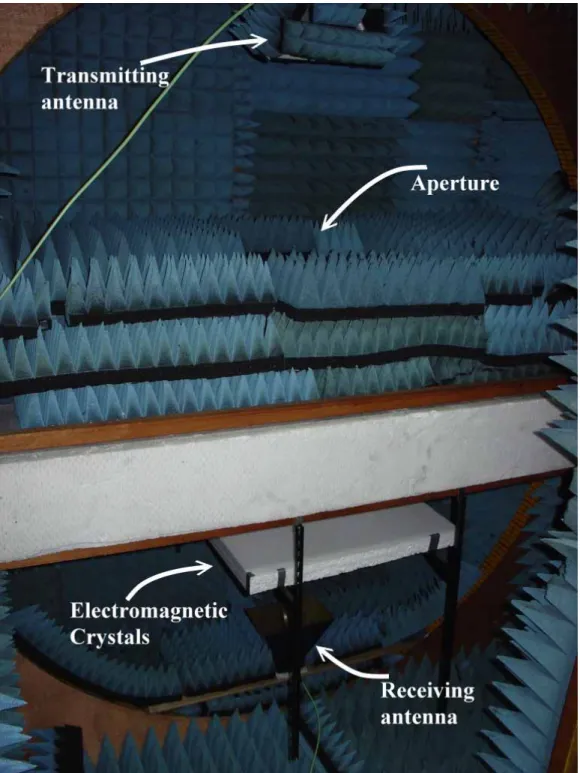
Referring to figure 3-1, a rectangular box, made of wood, equipped with foam absorbers has the dimension of 200, 123 and 240 cm for its width, depth and height, respectively. Such a kind of environment is called microwave anechoic chamber, which can suppress the multiple reflections from the walls and mimic the free space. Ideally, the microwave anechoic chamber can approach the behavior of free space. However, due to the limitation on its size and the quality of foam absorber, the performance of it is not so perfect; this will be obviously observed by the measurement data of propagation loss shown in the next section. Nevertheless, since the difference of propagation loss between theoretical calculation and experimental measurement is less than 5 dB, in the frequency range of our interest, which can
meet the specification of IEEE standard concerning anechoic chamber, this allow us to make certain the standard and consistent measurement in this thesis.
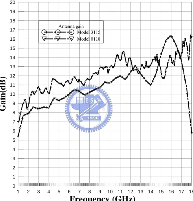
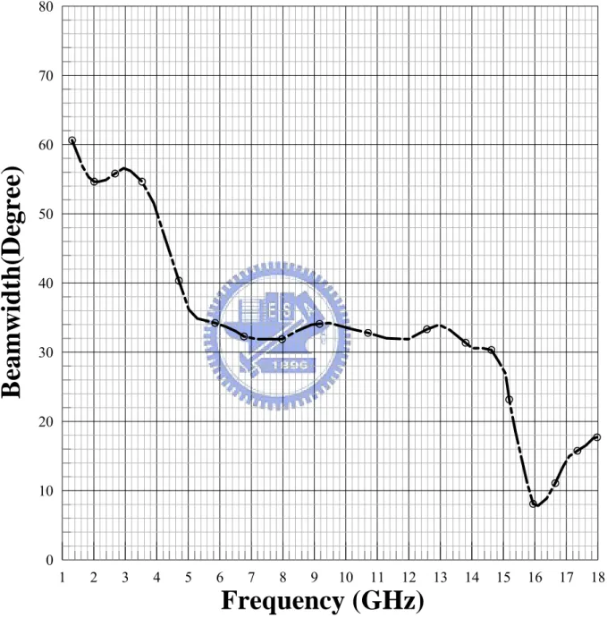
Double ridged horn antennas can keep high radiation efficiency in a wide frequency range; therefore, we can clearly inspect band structure of EM crystals including passband and stopband. Besides, the property of linear polarization with the antenna with allows us to simultaneously explore the scattering characteristics for both z- and x- polarized. As shown in the figure 2-2, the variation of antenna gains versus frequencies of operation for both horn antennas, model -3115 and -0118, are drawn according to the given specification. The two horn antennas have the antenna gain between 5.4 and 16.3 dB in the frequency range from 1 to 18 GHz. Besides, the antenna gains increases as the increasing in frequency, this is due to the large electrical lengths with the aperture in high frequencies. In addition, the two horn antennas are deployed in this chamber, with a precise alignment, as shown in figure 3-1. According to the equation 3-2, for a long distance communication system, the propagation loss appears to be apparently; the received power may have poor signal to noise ratio. In order to resolve this problem, we employ microwave power amplifier to enlarge the transmitted power before being radiated from the transmitting antenna.
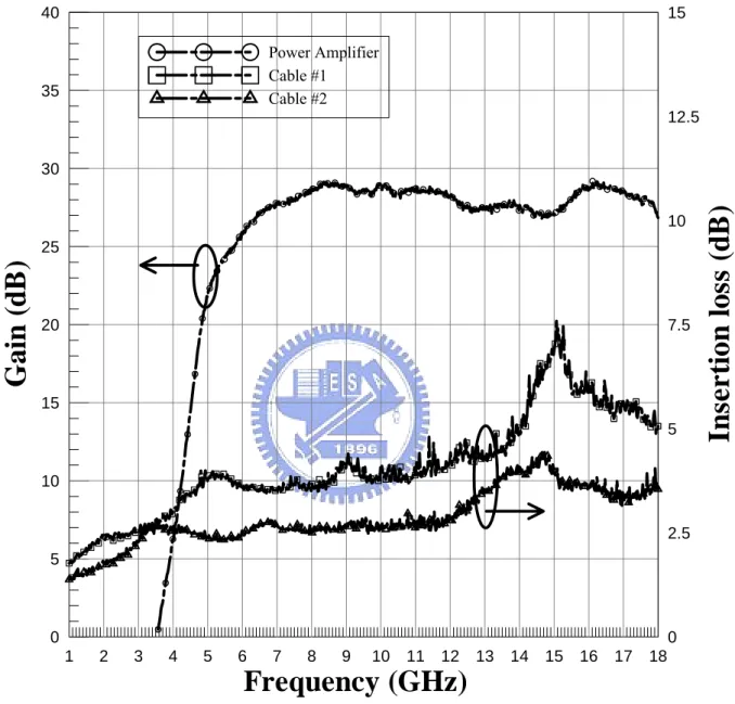
As shown in figure 3-3, it indicates the variation of amplifier gain versus frequencies of operation. For frequency below 3.5 GHz, the power amplifier does not work because of below-cutoff. For frequency from 5 to 18 GHz, the power amplifier has the stable gain between 22.5 and 29 dB, which can efficiently compensate the propagation loss to improve the signal to noise ratio.
Besides, the variation of the cable losses again the frequencies of operation is shown in the figure 3-4. Since the lengths of the two coaxial cables are different, the difference in cables losses is obvious in the figure. Furthermore, the cable loss increases as the increase in the frequency; this confirms the behavior of dielectric loss in high frequency.
In our experiment, HP 8722D, vector network analyzer (VNA), was employed to perform a close-loop measurement. The scattering parameters, including the return- and insertion- loss, represent the reflection and transmission efficiencies, respectively, of the plane wave by the sample under test.
Since the plane wave does not exist in practice, in order to have a consistent comparison between the theoretical calculation and experimental measurement, we must generate a
uniform plane wave in a finite cross section to model the plane wave in theoretical.
In our experiment, as shown in the figure 3-1, we carve out a rectangular hole from a foam absorber to act as an aperture. Since the absorbing material is employed, the wave illuminates on it will be absorbed, while the others will pass through. That is, the aperture used here is to serve as a mask to allow the transmission of uniform field while blocking the others away from the aperture. It is noted that the wave illumination on the aperture, in general, is a uniform plane wave of finite extent. The tapering in the field distribution on the aperture may cause slight difference in the results obtained from theoretical and experimental studies. Moreover, in the high frequency range, the high antenna gain means the narrow beam width, which results in the small area of illumination over the sample. Under this situation, the scattering characteristic is mainly contributed by a small part of a structure instead of the overall one, which will be evidently explored by the results in the following chapter. In a word, the criterion in designing the electromagnetic mask depends on two factors: one for the number of periods required along the transverse direction and the other for the field uniformity for the coverage with the electromagnetic beam.
3-4 Calibration Procedure
As described previously, the definition of antenna factor stands for the ratio of electric field strength on the aperture to the voltage at the load of antenna. Thus, to have the electric field strength at the input- and output- surface of the sample under test, we should transform the voltage measured by the VNA (the load of antenna) into the electric field strength on the aperture of horn antennas. Besides, the propagation loss from the aperture of antenna to the surface of sample should also be taken into account. Notice that the reference planes for the VNA are set at the end of the two flexible coaxial cables, therefore, the effects caused by cable losses and the amplifiers should be considered at the same time. In general, the electric field strength at the artificial surface away from the aperture of horn antenna is figured out by the following equation:
n propagatio amplifier cables dB G dB L L dB F A V db V m V dB E( µ / )= ( µ )+ . .( )+ ( )− ( )+ 3-3
Where the E represents the electric field strength at the prescribed artificial surface, which is measured by the unit of dBµV; V is the voltage measured by the VNA, and A. F. is the antenna
factor given by the specification of the horn antennas; Lcables is the loss due the coaxial cables,
and Gamplifier is the gain of the amplifier; Lpropagation is the propagation loss of plane wave.
antennas obtained from VNA. For the frequencies below 4 GHz, the power amplifier is below cutoff-frequency or poor in gain, the input signal from the VNA is blocked by the power amplifier. Besides, for the frequencies from 4 to 18 GHz, the amplifier is operation in the linear region. Therefore, when considering the limitation on the power amplifier and together with the beamwidth of horn antennas, the frequency range of measurement is chosen from 4 GHz to 14 GHz.
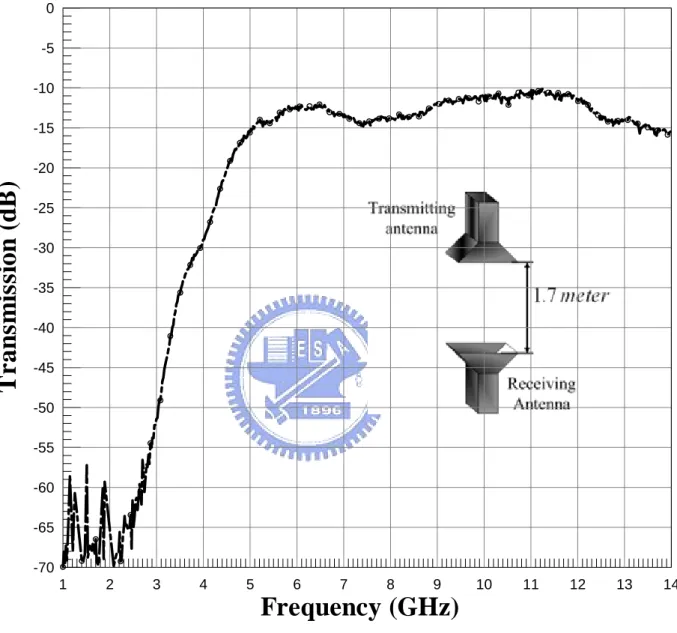
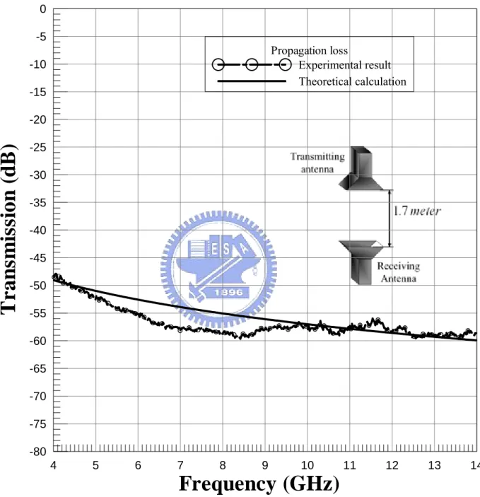
Substituting amplifier gain, losses of coaxial cables and antenna gains into the equation 3-4, we can achieve the experimental result of propagation loss. Besides, for this measurement system, the distance R between the two horn antennas was attached in the figure 3-1. We have the distance of 1.7 meter in equation 3-2 to obtain the theoretical calculation results, which are depicted in figure 3-6. It indicates that the anechoic chamber has variation in the propagation loss from -4 to 2.2 dB, in frequencies from 4 to 14 GHz. In general, the propagation loss has considerable agreement between theoretical calculation and experimental measurement.
So far, we have evaluated the performance of this anechoic chamber by examining the propagation loss of wave propagating in both theoretical and experimental ways. As this is done, we have a good position in the measurement of scattering characteristics for the EM crystals, since the side effects due to the propagation environment have been totally understood.
1 2 3 4 5 6 7 8 9 10 11 12 13 14 15 16 17 18
Frequency (GHz)
0 1 2 3 4 5 6 7 8 9 10 11 12 13 14 15 16 17 18 19 20Ga
in(
d
B
)
Antenna gain Model 3115 Model 01181 2 3 4 5 6 7 8 9 10 11 12 13 14 15 16 17 18
Frequency (GHz)
0 5 10 15 20 25 30 35 40Gai
n
(
d
B
)
0 2.5 5 7.5 10 12.5 15In
se
r
ti
o
n
l
o
ss
(d
B)
Power Amplifier Cable #1 Cable #21 2 3 4 5 6 7 8 9 10 11 12 13 14 15 16 17 18
Frequency (GHz)
0 10 20 30 40 50 60 70 80Beamwidth(Degree)
1 2 3 4 5 6 7 8 9 10 11 12 13 14
Frequency (GHz)
-70 -65 -60 -55 -50 -45 -40 -35 -30 -25 -20 -15 -10 -5 0T
r
an
sm
is
si
on
(
d
B
)
4 5 6 7 8 9 10 11 12 13 14
Frequency (GHz)
-80 -75 -70 -65 -60 -55 -50 -45 -40 -35 -30 -25 -20 -15 -10 -5 0T
r
an
sm
is
si
on
(
d
B
)
Propagation loss Experimental result Theoretical calculationFigure 3-6 Variation of propagation loss against the frequency ; results for measurement and calibration
Chapter 4: Experimental and numerical results
In this chapter, we will carry out the numerical simulation and experimental studies to realize the scattering characteristics of plane wave by an electromagnetic (EM) crystal. The testing facilities and their basic principles have been demonstrated in the previous chapters. To maintain the succinctness of this thesis, I will not describe them again here. On the other hand, according to the basic theory of periodic structure, for instance, at the Bragg condition, the in-of-phase reflection of the incident waves from each unit cell will result in the occurrence of stopband; namely, the strong reflection will be exhibited in such a frequency band. Contrast to it, the waves can penetrate into the EM crystal in the passband region. These scattering characteristics can be easily observed by the experimental studies.
To obtain a physical insight of wave processing in the EM crystal, in this thesis, we will employ the simulation program EMCRY, which is a full-wave simulation software based on rigorous mode-matching method incorporated with generalized eigen value problem, developed by R. B. Hwang [18]. By the parametric studies for the EM crystal, we could have a mutual examine between the theoretical and experimental results.
4-1 Scattering characteristics of a 2-D EM crystal
In our experiment, we have implemented two set of 1-D metal strips arrays: one for 10 mm in strip width and the other for 15 mm, however, the period retains to be 20 mm. The metal strip used in our experiment is made up of copper and silver foils. The thickness of them all is 0.06 mm. These metal strips are coated on the Polystyrene, which has the relative dielectric constant close to unity. Moreover, we have three thicknesses of the Polystyrene, which are 24 mm, 27 mm and 30 mm, respectively. Based on the structural parameters shown previously, we have several combinations for implementing the 2-D electromagnetic crystals. Notice that the definition of layer in this research is based on the number of 1-D metal strip arrays; that is, the 2-layer means that there are two 1-D metal strip arrays and one Polystyrene separator; the 4-layer represents four 1-D metal strip array and three Polystyrene separators, and vice versus. In the following experimental studies, we will have the 2-D EM crystals including two, four and six layers and measure its transmittance response under the condition of normal incidence. Besides, both the horizontal and vertical polarizations for the electric-field for the incident beam are performed. The horizontal (vertical) polarization corresponds to the x-polarized (z-polarized) one, which have been defined in the previous
chapter.
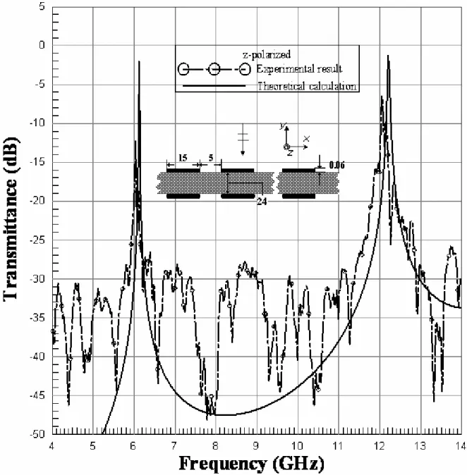
Figure 4-1 shows the variation of transmittance against frequency of operation for both theoretical and experimental results. The uniform plane wave is normally incident with z-polarized. The width of the metal strip and the period are 15 mm and 20 mm, respectively. The thickness of the separator is 24 mm. Besides, there is no lateral shift distance for these two 1-D metal strips arrays. As shown in this figure, the theoretical calculation depicts two transmission spikes around 6 GHz and 12.3 GHz, respectively. Although not shown the response below 4 GHz, since the transmittance below 6 GHz is very small, the 6 GHz can be considered as the cutoff frequency of this 2-D EM crystal. In addition, from the results shown in this figure, it can be conjectured that there are two pass bands (two stop bands and one below cutoff band) in the frequency of operation. The wave in the two pass bands exhibits apparently transmitting, however, strongly reflecting in the stop band and below-cutoff regions. This phenomenon can be obviously observed by the measured response as illustrated in this figure. The slight differences in the pass band frequency may be due to the following two parameters: one for the relative dielectric constant of the Polystyrene and the other for the taper plane wave.
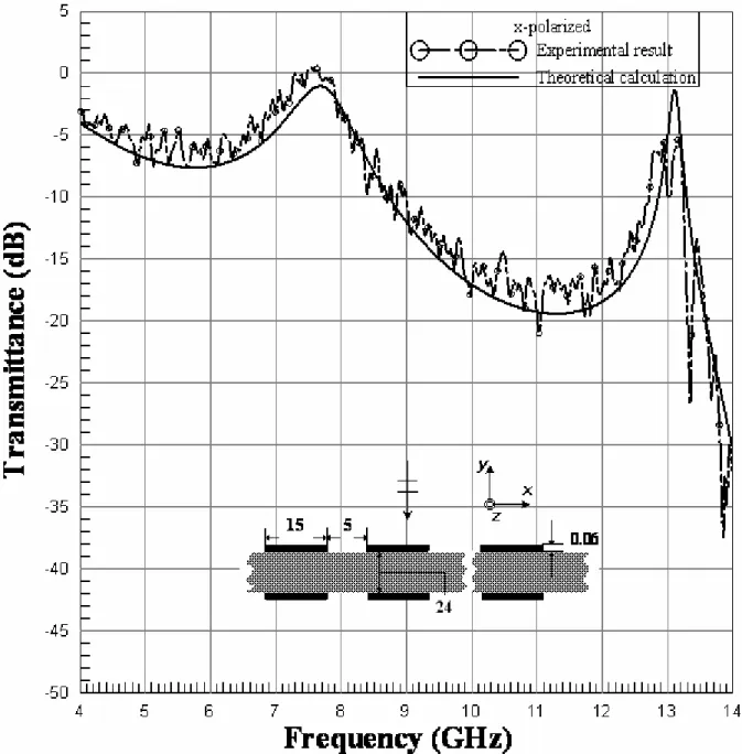
In the next experiment, we retain the structure under consideration; however, change the polarization into x-polarized. The results of theoretical and experimental studies are shown in figure 4-2. Compared with the previous figure, we found this structure seems to be more transparent for the x-polarized. This may be inferred as the statements given below.
The 2-D EM crystal typically can be regarded as the stacks of 1-D parallel-plate waveguide arrays. As we have known from the basic electromagnetic theory, the TE polarization (z-polarized) wave has cutoff frequency; on the contrary, TM polarization (x-polarized) can propagate down to DC. As described in the previous example, the cutoff frequency is around 6 GHz for the z-polarized, however, null for x-polarized.
In the following two examples, we change the metal strip width into 10 mm while the other parameters are the same. Since the aspect ratio for the metal (defined as the ratio of metal width to period) is smaller compared with that in the previous example, the transmittance should be more considerable than the former ones. We can confirm this viewpoint by the figures 4-3 and 4-4 for the z- and x- polarized wave incidences, respectively. Figure 4-3 and figure 4-4 show the same tendency as those in figure 4-1 and 4-2, respectively. It is worthy to note that the cutoff frequency for the z-polarized wave incidence shifts to the lower
frequency as shown in figure 4-3. This can be concluded as that the width parallel-plate waveguide increases and thus the cutoff frequency decrease accordingly, when compared with the two cases shown in figure 4-1 and 4-3.
In this example, we increase the number of 1-D metal strips arrays up to 3 layers. Also shown in figure 4-5, the cutoff phenomenon due to the parallel-plate waveguides array for z-polarized is present. Besides, the first stop band locates at almost the same region as shown in figure 4-3, while the attenuation is stronger than the previous case. This is because of the increase in the number of metal strips arrays. It is noted that in the vicinity of the band edges there are two ripples present, however, there is only one ripple in the previous case. As a thumb of rule, the number of ripples equals to N-1, where N is the number of metal strips arrays.
On the other hand, the result for x-polarized incident wave is shown in figure 4-6. From this figure, we observe that the tendency of the distribution for the transmittance is similar to the previous case of 2 layers, except for the strong attenuation around 11 GHz. This can be concluded as the stop band along y axis.
We continuously increase the number of metal strips array up to 4 layers. The transmittance for both z- and x- polarized of incident plane waves is shown in figure 4-7 and 4-8. From these two figures, we again confirm the existence of stop band by the stronger attenuation in that region. That is, in the stop band region, the degree of reflection is dependent on the number of metal strips arrays along y direction, however, the location of stop band remains the same. Besides, the number of ripples due to the multiple scattering inside the 2-D EM crystal could be determined by the number of metal-strip arrays along y direction only.
4-2 Scattering characteristic of a defect 2-D EM crystal
In recent years, many researchers found that defects in an electromagnetic crystal can drastically change its scattering characteristics. The defect could be obtained by slightly perturbing the structure, for instance, carve out a 1-D periodic layer or change the dielectric constant in a small region in a crystal. To mention a few, Hwang and et. al. [19] employed rigorous mode-matching method to prove the wave guiding in a defect 2-D photonic crystal. In their research report, the defect structure can be considered as a waveguide having the 2-D electromagnetic crystal as its side walls. As the crystal operates in stop band or below cutoff, the wave can bounce back and forth inside the channel. Besides, they also verify the
transmission spike inside a stop band by the dispersion relation of the waveguide. In this research, we have also explored the scattering characteristics of a defect EM crystal. The 2-D EM crystal having three metal strips arrays were taken as an example, wherein, the width of the second separator was changed to see the variation in its transmittance response.
Figure 4-9 shows the distribution of transmittance against frequency for a defect 2-D EM crystal. Most of the structural parameters are the same with those in figure 6, except for the thickness of the separator for the center one. This structure has a defect in the thickness of the separator, that is, the thickness of the central separator is 48 mm, different from the other ones. From this figure, we found that the location of stop band remains the same; nevertheless, there is a small region of pass band within it. Although not shown in this thesis, the transmission spike corresponds to the resonance frequency of the overall structure along y direction. At this frequency, the incident wave couples into the structure and again radiates into the environment (free space). Thus, if there is considerable loss in the separator, the incident power will be absorbed by the lossy medium. In a word, the transmission spike is due to the Wood’s anomalous, that is, the phase matching between the incident plane wave and the guided waves supported by the defect waveguide.
The transmission spike also occurs in the situation of x-polarized, which was depicted in figure 4-10. Since there is no other new physical phenomenon found in this figure, we will not make any comments on the result.
We again change the separation distance for the defect structure in the previous example. The distance was changed to 72 mm, which is triple of the other ones. The transmittance response for both z- and x- polarized are shown in figure 4-11 and 4-12, respectively. From these two figures, we found the good agreement between the measurement and computational results, in particular for the transmission spikes. Since the physical consequence for these spikes have been demonstrated in the previous examples, we will not address them again. However, it is worthy to note that the location of transmission spike coincides very well in this experiment when compared with the previous cases.
So far, we have examined the transmittance responses for the 2-D EM crystal having 2, 3 and 4 layers and those for the defect structures. The stop bands due to the periodicity along y direction have been illustrated by changing the number of period along that direction to see the variation on the transmittance. In the next example, we combine two types of 2-D EM crystals to form a composite structure and examine its transmittance characteristics. The
first one has the metal strip width 10 mm and 15 mm for the other one, while the two structures have the same period 20 mm along x direction. The transmitted responses are shown in figure 4-13 and 4-14 for z- and x- polarized, respectively. Since these two structures have almost the same tendency in the distribution of transmittance except for the attenuation in its stop band, the combination of the two structures will further enhance the capability frequency selectivity for the structure. As shown in the figure 4-13, there are two narrow transmission bands allow the wave to penetrate the structure, while the other frequency components were rejected. It indicates that such a structure can be employed as a dual band frequency selective surface (FSS) having very well selectivity in frequency. In generally speaking, the experimental results can approach the numerical ones in their tendency. However, due to the misalignment for the stack of 1-D metal strips arrays, the frequency shift in the results could be apparently observed. This could be further improved by fabricating the samples using semiconductor process in the future.
Figure 4-1 Variation of transmittance against frequency for both experimental measurement and theoretical calculations; z-polarized wave incidence; for two 1-D metal strip arrays
having the same metal width 15 mm, lateral shift 0 mm, separator 24 mm, and metal thickness 0.06 mm
Figure 4-2 Variation of transmittance against frequency for both experimental measurement and theoretical calculations; x-polarized wave incidence; for two 1-D metal strip arrays
having the same metal width 15 mm, lateral shift 0 mm, separator 24 mm, and metal thickness 0.06 mm
Figure 4-3 Variation of transmittance against frequency for both experimental measurement and theoretical calculations; z-polarized wave incidence; for two 1-D metal strip arrays
having the same metal width 10 mm, lateral shift 0 mm, separator 24 mm, and metal thickness 0.06 mm
Figure 4-4Variation of transmittance against frequency for both experimental measurement and theoretical calculations; x-polarized wave incidence; for two 1-D metal strip arrays
having the same metal width 10 mm, lateral shift 0 mm, separator 24 mm, and metal thickness 0.06 mm
Figure 4-5 Variation of transmittance against frequency for both experimental measurement and theoretical calculations; z-polarized wave incidence; for three 1-D metal strip arrays having the same metal width 10 mm, lateral shift 0 mm, separator 24 mm, and metal thickness 0.06 mm
Figure 4-6 Variation of transmittance against frequency for both experimental measurement and theoretical calculations; x-polarized wave incidence; for three 1-D metal strip arrays having the same metal width 10 mm, lateral shift 0 mm, separator 24 mm, and metal thickness 0.06 mm
Figure 4-7 Variation of transmittance against frequency for both experimental measurement and theoretical calculations; z-polarized wave incidence; for four 1-D metal strip arrays having the same metal width 10 mm, lateral shift 0 mm, separator 24 mm, and metal thickness 0.06 mm
Figure 4-8 Variation of transmittance against frequency for both experimental measurement and theoretical calculations; x-polarized wave incidence; for four 1-D metal strip arrays having the same metal width 10 mm, lateral shift 0 mm, separator 24 mm, and metal thickness 0.06 mm
Figure 4-9 Variation of transmittance against frequency for both experimental measurement and theoretical calculations; z-polarized wave incidence; for four 1-D metal strip arrays having the same metal width 10 mm, lateral shift 0 mm, and metal thickness 0.06 mm with different separator 24, 48 and 24 mm
Figure 4-10Variation of transmittance against frequency for both experimental measurement and theoretical calculations; x-polarized wave incidence; for four 1-D metal strip arrays having the same metal width 10 mm, lateral shift 0 mm, and metal thickness 0.06 mm with different separator 24, 48 and 24 mm
Figure 4-11 Variation of transmittance against frequency for both experimental measurement and theoretical calculations; z-polarized wave incidence; for four 1-D metal strip arrays having the same metal width 10 mm, lateral shift 0 mm, and metal thickness 0.06 mm with different separator 24, 72 and 24 mm
Figure 4-12 Variation of transmittance against frequency for both experimental measurement and theoretical calculations; x-polarized wave incidence; for four 1-D metal strip arrays having the same metal width 10 mm, lateral shift 0 mm, and metal thickness 0.06 mm with different separator 24, 72 and 24 mm
Figure 4-13 Variation of transmittance against frequency for both experimental measurement and theoretical calculations; z-polarized wave incidence; for six 1-D metal strip arrays having the same separator 24 mm, lateral shift 0 mm, and metal thickness 0.06 mm with different metal width 10, 10, 10, 10, 10, 15, and 15 mm
Figure 4-14 Variation of transmittance against frequency for both experimental measurement and theoretical calculations; x-polarized wave incidence; for six 1-D metal strip arrays having the same separator 24 mm, lateral shift 0 mm, and metal thickness 0.06 mm with different metal width 10, 10, 10, 10, 10, 15, and 15 mm
Chapter 5: Conclusion
In this thesis, we have implemented a test fixture and the 2-D EM crystals to measure its transmittance characteristics. To compare the experimental results with the theoretical ones on the same basis, the calibration procedure was made to transform the measured voltage at the load of VNA to the electric field strength on the two outer surfaces of EM crystal. In addition, the stop-band behavior was carefully examined by changing the number of periods along the direction of wave propagation. As confirmed by the measurements, the increase in the number of periods indeed enhances the attenuation in the stop band region. The good agreement between the measured and calculated results validates the scattering characteristics of the 2-D EM crystal and also proves the accurate of the experiment study in this thesis. Besides, the selectivity in the transmitted frequency bands for the structure under consideration also indicates the potential applications in FSS.
In a word, the contribution of this research work is to establish a consistent and standard procedure for measuring the scattering characteristics of a 2-D EM crystal. This work is the basis conducting to the understanding for the ultra-refraction phenomena behind an EM crystal.
References
[1] T. Tamir, H. C. Wang, and A. A. Oliner, “Wave propagation in sinusoidally stratified
dielectric media,” IEEE Trans. Microwave Theory Tech., vol. MTT-12, p. 323, May 1964. [2] A. Hessel and A. A. Oliner, “A new theory of Wood’s anomalies on optical gratings,”
Appl. Opt., vol. 4, pp. 1275–1297, 1965.
[3] S. T. Peng, T. Tamir, and H. L. Bertoni, “Theory of dielectric grating waveguides,” IEEE
Trans. Microwave Theory Tech., vol. MTT-23, pp.123–133, Jan. 1975.
[4] C. Elach, “Wave in active and passive periodic structures: A review,” Proc. IEEE, vol. 64, pp. 1666–1698, Dec. 1976.
[5] T. K. Gaylord and M. G. Moharam, “Analysis and applications of optical diffraction by gratings,” Proc. IEEE, vol. 73, pp. 884–937, Oct. 1985.
[6] R. C. Hall, R. Mittra, and K. M. Mitzner, “Analysis of multilayered periodic structures using generalized scattering matrix theory,” IEEE Trans. Antennas Propagat., vol. 36, pp. 511–517, Apr. 1988.
[7] D. Maystre, “Electromagnetic study of photonic band gaps,” Pure Appl. Opt., vol. 3, no. 6, pp. 975–993, Nov. 1994.
[8] Jordi Romeu and Yahya Rahmat-Samii, “A fractal based FSS with dual band
characteristics, ”Antennas and Propagation Society. IEEE International Symposium, Vol3, pp. 1734–1737, July 1999
[9] Te-Kao Wu, “Four-band frequency selective surface with double-square-loop patch elements,” IEEE Transactions on Antennas and Propagation, Vol. 42, Issue 12, pp. 1659 – 1663, Dec. 1994.
[10] H. Y. D. Yang, J. A. Castaneda, and N. G. Alexopoulos, “An integral equation analysis of an infinite array of rectangular dielectric waveguides,” IEEE Trans. Microwave Theory
Tech., vol. 38, pp. 873–880, July 1990.
[11] Dan Sievenpiper, Lijun Zhang, Romulo F. Jimenez Broas, Nicholas G. Alexopolous and Eli Yablonovitch, “High-Impedance Electromagnetic surfaces with a Forbidden
Frequency Band,” IEEE Transactions on Microwave Theory and Techniques, VOL 47, No 11, pp2059-2074, Nov. 1999
[12] V. Radisic, Y. Qian, R. Coccioli, and T. Itoh,” Novel 2-D photonic bandgap structure for microstrip lines,” IEEE Microwave Guided Wave Lett., vol. 8, pp. 69–71, Feb. 1998. [13] Ruey Bing Hwang; Song Tsuen Peng, “Guidance characteristics of two-dimensionally
periodic impedance surface,” IEEE Transactions on Microwave Theory and Techniques, Vol 47, Issue 12, pp 2503 – 2511, Dec. 1999
[14] Ruey Bing Hwang; Song Tsuen Peng, “Surface-wave suppression of resonance-type periodic structures,” IEEE Transactions on Antennas and Propagation, Vol 51, Issue 6, pp1221 – 1229, June 2003
[15] D. R. Smith, W. J. Padilla, D. C. Vier, S. C. Nemat-Nasser and S. Schultz, "Composite medium with simultaneously negative permeability and permittivity," Phys. Rev. Lett.,
vol. 84, no. 18, pp. 4184-4187, May 2000.
[16] J. B. Pendry, “Negative refraction makes a perfect lens,” Phys. Rev. Lett., 85, pp 3966-3969, 2000
[17] V. G. Veselago, “The electrodynamics of substances with simultaneously negative values of εand µ, Sov Phys Usp , pp 509–514, 1968
[18] Ruey Bing Hwang, “Relations Between the Reflectance and Band Structure of 2-D Metallodielectric Electromagnetic Crystals,” IEEE Transactions on Antennas and Propagation, Vol 52, Issue 6, pp 1454 – 1464, June 2004
[19] Ruey Bing Hwang; Song Tsuen Peng, “Scattering and guiding characteristics of waveguides with two-dimensionally periodic walls of finite thickness,” RADIO SCIENCE, VOL: 38, NO: 5, 1091, doi:10.1029/2002RS002847, 2003
![[2015-Fall] WNFA lab1 - CamCom](data:image/gif;base64,R0lGODlhAQABAIAAAP///wAAACH5BAEAAAAALAAAAAABAAEAAAICRAEAOw==)