IEEE ELECTRON DEVICE LETTERS, VOL. 28, NO. 11, NOVEMBER 2007 993
A Simple Spacer Technique to Fabricate Poly-Si
TFTs With 50-nm Nanowire Channels
Chia-Wen Chang, Student Member, IEEE, Chih-Kang Deng, Hong-Ren Chang,
Che-Lun Chang, and Tan-Fu Lei, Member, IEEE
Abstract—In this letter, polycrystalline-silicon thin-film
transis-tors (poly-Si TFTs) with 50-nm nanowire (NW) channels, which are fabricated without advanced photolithography by using a side-wall spacer-formation technique, are proposed for the first time. Because the polygate electrode is perpendicularly across poly-Si NW channels to form a trigatelike structure, the proposed poly-Si NW TFT owns outstanding gate controllability. In summary, a simple and low-cost scheme is proposed to fabricate high-perfor-mance poly-Si NW TFT suitable for future display manufacturing and practical applications.
Index Terms—Nanowire (NW), polycrystalline silicon (poly-Si),
sidewall spacer, thin-film transistors (TFTs), trigatelike structure.
I. INTRODUCTION
P
OLYCRYSTALLINE-SILICON thin-film transistors (poly-Si TFTs) have attracted much considerable attention because they could be integrated with peripheral driving circuits on a low-cost glass substrate in active-matrix liquid-crystal displays [1], [2]. In addition, poly-Si TFTs have the potential to be used in 3-D circuits, including vertically integrated SRAMs [3] and DRAMs [4]. Recently, a lot of effort have been given to improve the gate controllability and device performance by changing device structure of poly-Si TFTs with complicated steps, such as the gate-overlapped lightly doped drain TFT [5], the double-gate TFT [6], and the gate-all-around TFT [7]. Moreover, poly-Si TFTs with nanoscale feature sizes have also been proposed to reduce the influence of the grain-boundary defects [8]–[12]. In these studies, the electrical performance of TFT could be remarkably improved by decreasing the channel dimensions to be comparable to, or still smaller than, the grain size. However, the poly-Si TFTs with narrow-width channels are directly defined by using costly electron-beam-lithography technology [8]–[10], which could not be practicable in flat-panel displays. On the other hand, for the poly-Si TFTs with nanowire (NW) channels and multiple-gate configuration reported in [11] and [12], the gate-induced drain-leakage (GIDL) current that resulted from largeManuscript received July 3, 2007. This work was supported in part by the National Science Council, Taiwan, R.O.C., under Contact NSC 95-2221-E-009-279 and in part by Chunghwa Picture Tubes (CPT), Ltd., Taiwan, R.O.C. The review of this letter was arranged by Editor J. Sin.
The authors are with the Institute of Electronics, National Chiao-Tung University, Hsinchu 300, Taiwan, R.O.C. (e-mail: [email protected]).
Digital Object Identifier 10.1109/LED.2007.906808
gate-to-drain overlapping area is high and must be addressed by additional processes. Furthermore, in order to form a trigate structure with NW channels, the extra top metal gate and bottom Si-substrate gate accompanied with high-temperature thermal-oxide and rapid-thermal processing are used [10], [11], which are difficult to process in liquid-crystal display (LCD) production line.
In this letter, we proposed a simple spacer technique to fabricate high-performance poly-Si TFTs. The self-aligned for-mation of twin poly-Si NWs with 50-nm linewidth is directly defined to serve as the channel regions without any expensive photolithography process. All processes are compatible with modern LCD production line and suitable for system-on-panel (SOP) applications in the future.
II. DEVICEFABRICATION
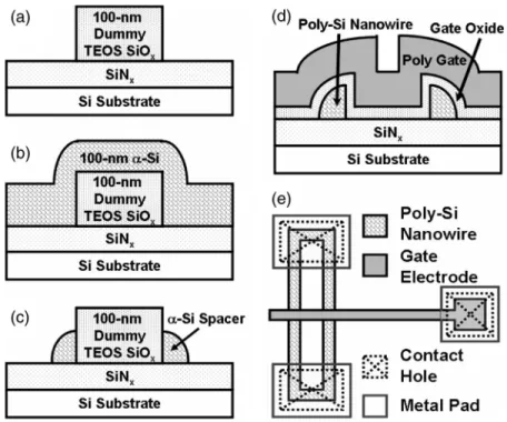
The major processes to fabricate the proposed poly-Si NW TFT by a sidewall spacer-formation technique are depicted in Fig. 1(a)–(e) shows the device top view. First, a 150-nm-thick SiNX and a 100-nm-thick tetraethooxysilane (TEOS) SiOX
were consecutively deposited by plasma-enhanced chemical-vapor-deposition (PECVD) system to serve as the starting substrate and the dummy oxide layer, respectively. After pat-terning the dummy oxide stripe [Fig. 1(a)], a 100-nm-thick amorphous-silicon (α-Si) film was deposited by low-pressure CVD (LPCVD) [Fig. 1(b)] and, then, anisotropically etched to form α-Si spacer (namely, α-Si NW) in a self-aligned man-ner without extra mask or advanced photolithography system [Fig. 1(c)]. The feature size of the α-Si NWs could be well controlled by the thickness of α-Si film and the dry-etching condition. Next, a solid-phase-crystallization annealing was executed at 600 ◦C for 24 h in N2 ambient to transform the
α-Si into poly-Si. Then, the dummy oxide stripe was removed
by buffered-oxide-etchant solution, and then, the square-coil poly-Si NW was reserved [Fig. 1(e)].
Afterwards, a 34-nm-thick TEOS gate oxide was deposited by PECVD system, and a 250-nm-thick phosphorus-doped poly-Si was then deposited by LPCVD system to serve as the gate electrode [Fig. 1(d)]. Subsequently, a self-aligned phosphorus-ion implantation was performed at the dosage and the ion energy of 5× 1015cm−2and 15 keV, respectively, and then, the source/drain dopants were activated by an annealing treatment at 600 ◦C for 12 h in N2 ambient. After deposit-ing the passivation layer and defindeposit-ing the contact holes, the 500-nm-thick Al electrodes were deposited and then patterned
994 IEEE ELECTRON DEVICE LETTERS, VOL. 28, NO. 11, NOVEMBER 2007
Fig. 1. (a)–(d) Cross-sectional views of the major processes to fabricate the poly-Si NW TFT. (e) Schematic top view of the proposed poly-Si NW TFT.
Fig. 2. (a) Cross-sectional TEM micrograph of the test structure of the proposed poly-Si TFT having a couple of NW channels with a 300-nm distance. (b) Fractional enlarging plot in (a).
[Fig. 1(e)]. Finally, a NH3 plasma treatment was performed at 300◦C for 1 h to improve the device performance.
III. RESULTS ANDDISCUSSION
Fig. 2(a) shows the cross-sectional transmission-electron-microscopy (TEM) micrographs of the test structure of the proposed poly-Si TFT with NW channels. Here, such test structure with a small dimension of 300-nm distance is used to make the illustration clearer. The fractional enlarging plot of poly-Si NW channel is shown in Fig. 2(b). Because the polygate pattern is perpendicularly across poly-Si NW, a couple of active channels would be formed after removing the dummy oxide stripe in the proposed poly-Si NW TFT. From the cross-sectional TEM micrograph, the vertical sidewall thickness (TSi) and horizontal width (WSi) are approximately 50 nm. The aspect ratio TSi/WSi of the active channel in the poly-Si NW TFT (approximately equals to one) is larger than
Fig. 3. Typical transfer characteristics of the proposed poly-Si NW TFT, with and without NH3plasma treatment for 1 h. The inset table is the electrical
characteristics comparison of the poly-Si NW TFT, with and without NH3
plasma treatment for 1 h.
that in the traditional planar TFT (much smaller than one). Such high aspect ratio means that the gate electrode forms in a trigatelike structure with well electrostatic controllability on channel potential due to sidewall and corner contribution effects [13], [14].
Typical transfer characteristics (IDS−VGS) of poly-Si NW TFTs, with and without NH3 plasma treatment, are compared and shown in Fig. 3. The effective channel width of the poly-Si NW TFTs is defined as twice the horizontal width (2× WSi) of 100 nm parallel on the starting substrate, which is the same definition in other reports on TFT field [8]–[10]. TheON/OFFcurrent (ION/IOFF) ratio is the ratio of the max-imum ON-state current to the minimum OFF-state current at
CHANG et al.: SIMPLE SPACER TECHNIQUE TO FABRICATE POLY-Si TFTs WITH 50-nm NANOWIRE CHANNELS 995
VDS= 0.5 V. The threshold voltage (VTH) is defined as the gate voltage required to achieve a normalized drain current of
IDS= (W/L)× 100 nA at VDS= 0.5 V. After NH3 plasma passivation for 1 h, the threshold voltage is scaled down from 2.2 to 0.3 V, the field-effective mobility (µFE) can be improved from 46.7 to 63.5 cm2/V· s, the subthreshold swing is also decreased from 570 to 170 mV/dec, and the ON/OFF current ratio could be increased one order of magnitude. In addition, the GIDL current could be suppressed near half order of mag-nitude at VDS= 3 V and VGS=−4 V. All of these devices’ parameters are summarized in the inset of Fig. 3.
Besides excellent gate controllability due to 3-D trigate feature, the effect of grain boundaries in poly-Si NW film also plays an important role. As the poly-Si TFTs are scaled down, the number of grain boundaries is decreased to dominate on the VTH decreasing [15], [16]. Therefore, in the poly-Si NW channel, the fewer grain boundaries make lower VTH for ploy-Si TFT, which obtains higher driving current under the same operational condition. On the other hand, according to the poly-Si model [17], the effective mobility (µFE) could be given as
µEF=
1
1 + (µG/µGB)[nLGB/L] exp[qVb/kT ]
(1) where µFEis the effective field-effect mobility, LGBis the av-erage boundary length, n = L/LG is the avav-erage grain-boundary number, and LG is the average intragrain length.
If the active channel is shrunk down to nanoscale dimension, the n value would be decreased to improved µFE [15], [17]. Finally, fewer grain boundaries in poly-Si NW channel also make effectively passivated deep-states by NH3 plasma treat-ment. Therefore, the high-performance poly-Si NW TFT with NH3plasma treatment could be achieved by utilizing a simple spacer-formation technology and suitable for LCD practical manufacturing.
IV. CONCLUSION
We have introduced a simple, low-cost, and self-aligned spacer technique to fabricate the poly-Si TFTs with NW chan-nels in this letter. The 50-nm NW channel could be easily real-ized by anisotropically etched without extra mask or advanced photolithography system. The proposed poly-Si NW TFT has excellent gate controllability due to the trigatelike structure with the sidewall and corner contribution effects. Besides, the fewer grain boundaries in poly-Si NW channel also improve the electrical characteristics of TFT, even including the effec-tively passivated deep-states by plasma treatment. Therefore, the proposed poly-Si NW TFT is highly suitable for realizing SOP applications.
ACKNOWLEDGMENT
The authors would like to thank the National Nano Device Laboratories (NDL) and the Nano Facility Center of the Na-tional Chiao-Tung University for the apparatus support.
REFERENCES
[1] T. Uchida, “Present and future trend of electron device technology in flat panel display,” in IEDM Tech. Dig., 1991, pp. 5–10.
[2] K. Chung, M.-P. Hong, C.-W. Kim, and I. Kang, “Needs and solutions of future flat panel display for information technology industry,” in IEDM Tech. Dig., 2002, pp. 385–388.
[3] A. O. Adan, K. Suzuki, H. Shibayama, and R. Miyake, “A half-micron SRAM cell using a double-gated self-aligned polysilicon pMOS thin film transistor (TFT) load,” in VLSI Symp. Tech. Dig., 1990, pp. 19–20. [4] H. J. Cho, F. Nemati, P. B. Griffin, and J. D. Plummer, “A novel pillar
DRAM cell for 4 Git and beyond,” in VLSI Symp. Tech. Dig., 1998, pp. 38–39.
[5] K. Ohgata, Y. Mishima, and N. Sasaki, “A new dopant activation tech-nique for poly-Si TFTs with a self-aligned gate-overlapped LDD struc-ture,” in IEDM Tech. Dig., 2000, pp. 205–208.
[6] Z. Xiong, H. Liu, C. Zhu, and J. K. O. Sin, “A new polysilicon CMOS self-aligned double-gate TFT technology,” IEEE Trans. Electron Devices, vol. 52, no. 2, pp. 2629–2633, Dec. 2005.
[7] S. Miyamoto, S. Maegawa, S. Maeda, T. Ipposhi, H. Kuriyama, T. Nishimura, and N. Tsubouchi, “Effect of LDD structure and channel poly-Si thinning on a gate-all-around TFT (GAT) for SRAMs,” IEEE Trans. Electron Devices, vol. 46, no. 8, pp. 1693–1698, Aug. 1999. [8] C.-P. Lin, B.-Y. Tsui, M.-J. Yang, R.-H. Huang, and C.-H. Chien,
“High-performance poly-silicon TFTs using HfO2 gate dielectric,” IEEE Elec-tron Device Lett., vol. 27, no. 5, pp. 360–363, May 2006.
[9] Y.-C. Wu, T.-C. Chang, P.-T. Liu, C.-S. Chen, C.-H. Tu, H.-W. Zan, Y.-H. Tai, and C.-Y. Chang, “Effects of channel width on electrical char-acteristics of polysilicon TFTs with multiple nanowire channels,” IEEE Trans. Electron Devices, vol. 52, no. 10, pp. 2343–2346, Oct. 2005. [10] Y.-C. Wu, T.-C. Chang, P.-T. Liu, Y.-C. Wu, C.-W. Chou, C.-H. Tu,
J.-C. Lou, and C.-Y. Chang, “Mobility enhancement of polycrystalline-Si thin-film transistors using nanowire channels by pattern-dependent metal-induced lateral crystallization,” Appl. Phys. Lett., vol. 87, pp. 143 504-1–143 504-3, 2005.
[11] H.-C. Lin, M.-H. Lee, C.-J. Su, and S.-W. Shen, “Fabrication and char-acterization of nanowire transistors with solid-phase crystallized poly-Si channel,” IEEE Trans. Electron Devices, vol. 53, no. 10, pp. 2471–2477, Oct. 2006.
[12] C.-J. Su, H.-C. Lin, H.-H. Tsai, H.-H. Hsu, T.-M. Wang, T.-Y. Huang, and W.-X. Ni, “Operations of poly-Si nanowire thin-film transistor with a multiple-gated configuration,” Nanotechnology, vol. 18, no. 21, p. 215 205, May 2007.
[13] M. C. Lemme, C. Moormann, H. Lerch, M. Moller, B. Vratzor, and H. Kurz, “Triple-gate metal-oxide effect transistors fabricated with inter-ference lithography,” Nanotechnology, vol. 15, no. 15, pp. S208–S210, 2004.
[14] J.-W. Yang and J. G. Fossum, “On the feasibility of nanoscale triple-gate CMOS transistors,” IEEE Trans. Electron Devices, vol. 52, no. 6, pp. 1159–1164, Jun. 2005.
[15] S. Chopra and R. S. Gupta, “An analytical model for current-voltage char-acteristics of a small-geometry poly-Si thin-film transistor,” Semicond. Sci. Technol., vol. 15, no. 11, pp. 1065–1070, Nov. 2000.
[16] N. Yamauchi, J. J. Hajjar, and R. Reif, “Drastically improved performance in poly-Si TFTs with channel dimensions comparable to grain size,” in IEDM Tech. Dig., 1989, pp. 353–356.
[17] F. V. Farmakis, J. Brini, G. Kamarinos, C. T. Angelis, C. A. Dimitriadis, and M. Miyasaka, “On-current modeling of large-grain polycrystalline silicon thin-film transistors,” IEEE Trans. Electron Devices, vol. 48, no. 4, pp. 701–706, Apr. 2001.