Transistors Using Ion Plating Method
Ching-Fa Yeh, Tai-Ju Chen,t and Ming-Tyang unDepartment of Electronics Engineering and Institute of Electronics, National Chiao-Tung University, Hsinchu, Taiwan
.Jiann-Shiun Kao
Precision Instrument Development Center; National Science Council, Taiwan ABSTRACT
A novel method has been developed for efficiently reducing defect density in polysilicon thin film transistors using ion plated oxides as capping layers. The characteristics of these novel thin film transistors are superior to those of thin film transistors with plasma-enhanced chemical vapor deposited tetraethylorthosilicate capping oxides due to an in situ 02-plasma passivation effect during ion plating oxide deposition. The passivation effect of a NH3 plasma on the novel devices was also studied. The in situ ion plating 02 plasma shows a better passivation efficiency on trap states than the NH3 plasma. Polysilicon thin film transistors with ion plating capping oxides are hardly degraded even when stressed with a bias of 20 V at 100°C.
Introduction
It
is well known that polycrystalline silicon (poly-Si) films have a high concentration of grain boundary defects as well as intragrain defects. As a result of the highdensi-ty of trapping states in poly-Si films, it has been found
necessary to passivate them to improve poly-Si thin film transistor (TFT) performance."2 Various technologies have been proposed to reduce trapping states in poly-Si films, such as hydrogenation,'-4 03 plasma,5 and NH3 plasma.6 So far, the most popular passivation procedure has been to expose devices to hydrogen plasma. However, it takes a
long time to achieve satisfactory performance, and the
improvement shows a tendency to saturate.4 In addition, hydrogenated TFTs are quite prone to reliability problems due to carrier-induced trap states in poly-Si channels.78 These shortcomings greatly limit the practical application of H5-plasma passivation. In recent years, the passivation
effect of an 02 plasma has attracted much attention
because of its better passivation efficiency and stability.5 It has been suggested that 07-plasma treatment can improvethe performance of poly-Si TFTs by passivating deep states and tail states. Furthermore, it has been reported
that after an 03-plasma treatment, subsequent treatment with a H3 plasma was even more efficient in passivating trap states in poly—Si films.5
Recently, a low-temperature ion plating (IF) method has been proposed to prepare high-performance oxide films. IF oxide has been shown to be feasible for application as a poly-Si TFT gate insulator, and to contribute to excellent device characteristics.9 Since an 07 plasma is present in the chamber during IF oxide deposition, it can be expect-ed to have the effect of trap-state passivation on the poly-Si layer. In this paper, we try to apply IF oxides as capping layers on poly-Si TFrs, and investigate passivation effects owing to the in situ 03 plasma. The passivation of dangling bonds is examined by electron spin resonance (ESR) meas-urement.'°" NH3-plasma passivation effects and the relia-bility of the novel poly-Si TFTs are also studied.
Experimental
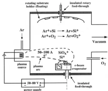
Preparationof IP oxide.—IF oxide films were prepared using the ion-plating system (Balzers BAP 800),"' shown
in Fig. 1. The starting silicon material was evaporated using an electron-beam evaporator. Simultaneously the
evaporator crucible served as the anode for an argon
plas-ma discharge. The high arc current was 56 A, while the
low arc voltage (Va,,) was 66 V and the anode-to-ground voltage (Vaflode) was46 V. Argon at 3.9 mbar in the plasma
*ElectrochemicalSociety Student Member.
source cavity was ionized by the heated filament, and it
was at 3.4 X
1O
mbar in the deposition chamber. Oxygen gas was let directly into the deposition chamber to fix thedeposition pressure at 1.1 X 1O' mbar, while the base
pressure was 3.6 X iO mbar. The evaporant (Si) and the reactive gas (02) were activated and ionized by the argon
plasma. The substrate holder was electrically isolated
from the ground chamber without an applied bias, i.e., it
was allowed to float. The substrate gathered electrons
from the plasma sheath, and then obtained a negative self-bias (V,) of —10 to —20 V (the body of the plasma). This negative bias accelerated the positive ions of the evapo-rant (Si), the reactive gas (07), and the argon plasma onto the surface of the substrate, and the film formed. The pos-itive ions tended to neutralize the received electrons, but the substrate was able to gather additional electrons from
the plasma sheath immediately. The IF oxide film was
deposited at a rate of 0.2 nm/s. No heater was applied to the substrate holder during deposition.
In conventional IF system the degree of ionization is too low to effectively deposit film, so the accelerating voltage must be rather high (generally 3 — 5 kV with a current
density of 0.3 —0.8mA/cm2) to supply sufficient energy.'4"5 In addition, the small quantity of ions is also disadvanta-geous for a reactive gas process. To overcome these
prob-Fig. 1. Schematic diagram of the ion-plating system (Baizers
BAP 800). Ar
I
Ar+Si —
Ar+Si Ar++02 Ar+02+ "acuum .4-021.483 4.9 8.5 X10⁻¹⁰ 9.3 4.5 —0.67 1.83 X 10" 1.463 2.0 1.1x iO-9.4 3.9 —1.68 4.50X 10 Table I. Physicochemical and electrical properties of IP and
thermal oxides.
Ion plating oxide Thermal oxide
1076
FTIR stretching frequency 1056
(cm)
Refractive inçlex P-etch rate (A/s)
Leakage current density
at 4 MV/cm (A/cm2)
Dielectric breakdown field
(MV/cm)
Dielectric constant at 1 MHz Flatband voltage (V) Interface state density
(eV' cm2)
Resultsand Discussion
IFoxide characteristics.—Table I summarizes the
typi-cal physicochemitypi-cal and electritypi-cal properties of 97 nm thick IP oxide deposited at room temperature. Those of
thermal oxide (—97 nm) grown in dry 02 at 1000°C are also shown for comparison. These two kinds of oxides were all prepared on 3 in. p-type (100)Si substrates. The thickness and the refractive index were measured by ellipsometer,
while the chemical structure was analyzed by Fourier
transform infrared spectrophotometer (FTIR). The etching
rate was examined with P-etch solution (48% HF: 70%
HNO3: H20 = 3:2:60)at room temperature. To investigate
the electrical properties of these oxides, metal-oxide-sili-con (MOS) capacitors with aluminum gates were prepared. The current-voltage (I-V) and capacitance-voltage (C-V)
characteristics were measured with an HP4145B and a
Keithley Package 82 system, respectively.0 The IP oxides have a lower FTIR stretching frequency, a higher
refrac-tive index, a higher P-etch rate, and a higher dielectric
constant. These features suggest that IF oxide is a
high-density material with strained bonds.9"" The electrical
properties of IF oxide are comparable to those of thermal
oxide, and include low leakage current, high dielectric
breakdown field, and few oxide charges. These excellent properties suggest that IP oxide is feasible for application as a capping layer in poly-Si TF'I's.
Characteristics of poly-Si TFTs with IP oxides as cap-ping layers.—Figure 3 shows the transfer characteristics of both poly-Si TFTs (W/L = 20/5 p.m) with IF and with TEOS oxides as capping layers, respectively. The charac-lems, a new IF system of BAP 800 has been developed.16 In
this new system the evaporant and the reactive gas can be effectively ionized and activated by a low-voltage (50 — 80V) high-current (50 — 100A) plasma arc. The arc
cur-rent can be controlled directly, while the resultant arc
voltage is also monitored. With respect to ground, a posi-tive potential (Vane) of 40 —60V is applied to anode. It is
recommended to have a potential difference of +20 V
between Vs,.. and Positive ions (Ar, evaporant, and
reactive gas) will be accelerated to the substrate holder
owing to a negative self-bias (—10 to —20 V) V =V,,— Vf, where V and Vf are the plasma and the substrate floating potential, respectively. The film quality is thus improved
because of high-energy atoms and the high-reactivity
plasma.
Fabrication of poly-Si TFTs.—Conventional co-planar N-channel poly-Si TFTs were prepared using the follow-ing procedures. The cross-sectional structure of the poly-Si TFI's is shown in Fig. 2. A 100 nm thick low-pressure chemical vapor deposition (LPCVD) amorphous Si layer was deposited on thermal oxide at 550°C using SiH4 gas. Recrystallization was performed at 600°C for 24 h using the solid-phase crystallization (SPC) method. A 40 nm thick liquid-phase deposited (LPD) oxide layer'8 was grown on the island-patterned SPC layer at 18°C, and then densified at 600°C for 1 h in 02 ambient. A 300 nm thick poly-Si layer was deposited using the LPCVD method at 620°C.
After the poly-Si gates were patterned, the source/drain and gate regions were implanted with phosphorus ions
(40 keV, 5 x 10'" cm2) by self-aligned technology. Dopant activation was performed at 600°C for 24 h in N, ambient. The 500 nm thick capping layer was deposited at a rate of 0.2 nm/s for about 42 mm using the IP method. The tem-perature of the substrate was 23°C at the beginning of the IP oxide deposition process, and increased to 110°C at its end. After contact holes were opened, aluminum electrodes were prepared and sintered at 400°C for 30 mm in N2 ambi-ent. The maximum processing temperature was 620°C.
For comparison, poly-Si TFTs with 32.5 nm thick LPD
gate oxides and 500 nm thick tetraethyl orthosilicate
(TEOS) capping oxides were prepared. The TEOS oxide was deposited at 300°C using the plasma-enhanced CVD
(PECVD) method. Hydrogenation by the NH3-plasma treatment was performed in a parallel-plate reactor at
300°C with a power density of 0.7 W/cm2.
ESR measurements—The dangling bond density in poly-Si films was measured by room-temperature ESR absorption spectra (X-band) before and after the in situ
02-plasma treatment. Poly-Si films were prepared by the LPCVD method at 620°C to a thickness of 300 nm onto
thermally oxidized Si-wafer. IP oxide was directly
deposited on the poly-Si films, and then annealed at 400°C for 30 mm in N, ambient. This is because devices were sin-tered after metallization in TFT fabrication processes. The deposition condition of IP oxide was the same as that of the IP capping oxide for poly-Si TFTs. Before ESR meas-urements, the IP oxide and the back side poly-Si/thermal oxide were removed.Capping
Layer
Fig.2. Cross-sectional structure of the poly-Si TFTs.
i o
,,
.5 10 I'.)-10
-5
05
10 15 20Gate
Voltage Vgs (V)
Fig. 3. Typical transfer characteristics (ld,-V9J at V,, = 15 V for poly-Si TFTs (W/L = 20/5 m) with IP and with TEOS oxides as capping layers without hydrogenation.
Table II. Device characteristic parameters for poly-Si TFTs (W/L =
20/5 jim) with IP and with TEOS capping layers before and after
8 h NH3-plasma treatment. Capping layer NHr plasma treatment V,1(V) S.S. (V/dee) ]I,,/I,,, (cm7V s) (cm3)N, 'P
teristics were measured at Vd, = 15V before hydrogenation.
The IP capped device obviously exhibits better
perfor-mance than that of the TEOS capped device, even when the TEOS capped device has a thinner LPD gate insulator. The key characteristic parameters of the two samples are sum-marized in Table II. Compared to the TEOS capped device, the IP capped device shows a smaller threshold voltage (Vth) of 4.23 \ a smaller subtbreshold swing (S.S.)of0.94V/dec,
a higher on/off current ratio (I/I) of 4.10>( i05, and a
higher field-effect mobility (p.FE)of24.3cm2/Vs. It is
evi-dent that the use of IP capping oxides indeed improves the performance of poly-Si TFTs. The above-mentioned
supe-rior device characteristics suggest that the IP capped
device has a lower trap-state density (N,) in the poly-Si channel. We can further calculate the effective trap-state density using the modified Levinson theorem.2''21 The N1 in the IP capped device is 1.05 x 1013 cm2,while it is 2.70 X
1013 cm2 in the TEOS capped device. We believe that the decrease in N1 for the IP capped device can be attributed
to the effect of in situ 03-plasma passivation during the
deposition of IF capping oxides.
To directly evaluate the variation of defects after the in situ 03-plasma treatment, dangling bond density in poly-Si films was also measured using ESR. Figure 4
shows the ESH absorption spectra with a resonance at g =
2.0055 for the poly-Si films before and after capping IP
oxide. The 5511 signal intensity decreases after capping IP
oxide, which indicates the reduction of the spin density (N,) in poly-Si films. N, is 6.68 x i0' cm3 for the fresh
specimen (before capping IP oxide), while it is5.32 x loll cm3 for the IP capped specimen before annealing. It is
evident that Si dangling bonds decrease after capping IP oxide. Moreover, N, is further reduced to 3.12>< l0cm3 for the IP capped specimen after 400°C annealing. The anneal enhances oxygen diffusion and passivation
effi-ciency. Hence, we can demonstrate that IP capping oxide indeed possesses passivation effects.
0
5 10 15 20
Gate Voltage Vgs (V)
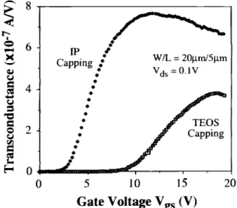
Fig. 5. Transconductance (Gm) as a function of gate bias at Vd, =
0.1 V for poly-Si TFTs (W/L = 20/5 jim) with IP and with TEOS oxides as capping layers.
Figure 5 shows transconductance (Gm) as a function of gate bias measured at V1, =0.1V for both IP capped and TEOS capped poly-Si TFTs (W/L =20/5 jIm). The maxi-mum Gm is 7.6 x lO A/V for the IF capped device, while it is 3.8 X 10 A/V for the TEOS capped device. In addi-tion, the gate voltage yielding the maximum Gm is also
comparatively small for the IP capped device. Figure 6
shows the output characteristics (Id,-Vd,) with V51-V,h =2V
and 6 V for both IP capped and TEOS capped devices
(W/L =20/10 p.m). In the curves of IP capped device, both
the high slope in the linear region and the high saturation current imply that channel conductance is high. Generally in poly-Si TFTs, the transport of free carriers between the
grains is impeded by the potential barrier owing to the
trap states at the grain boundaries.32'13 The lower barrier height makes On-state performance respond much faster
to the applied gate and drain biases. In the IF capped device, the increases in transconductance and channel
conductance can be attributed to the lowering of barrier height due to the reduction of trap-state density.
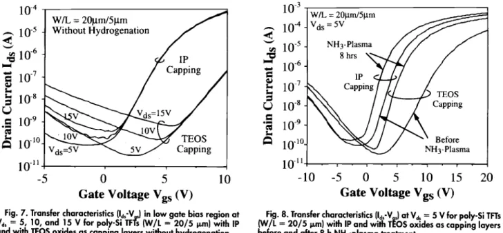
Figure 7 shows the transfer characteristics in the low
gate bias region at Vd, =5,10, and 15 V for both IP capped
40
a
'—' 30 J2 Pt C V0
1
C0
C 10 No 4.23 0.94 4.10 x 10' 8 h 2.33 0.77 3.18 x 10' TEOS No 11.0 1.61 2.09 x 101 8 h 5.49 0.84 4.75 x 101 24.3 1.05 x iO 28.6 8.37 ><iO
9.71 2.70 x i0' 14.4 1.05 x 10" Ip,,
W/L 201.tnlJSRmCapping /
•
Vds=O.lV.
•
4
2
•
..
•
•
..
0
Fresh•
IP Cappingg 2.0055
IP Capping & 400°C AnnealingSc
2.015 2.010 2.005 2.000 1.995g-value
Fig. 4. ESR absorption spectra with a resonance at g = 2.0055 for the poly-Si films before and after capping lP oxide.
0
0
2
4
6 8 10 12Drain Voltage Vds (V)
Fig.6. Output characteristics (la,-Vdj with VgsVi, as a parameter
for poly-Si TFTs (W/L = 20/10 jim) with IP and with TEOS oxides as capping layers.
and TEOS capped poly-Si TFTs without hydrogenation (W/L = 20/5 jim). In the case of Vd, =5V, the IP capped device shows a rather flat leakage characteristic
indepen-dent of gate bias except for a higher minimum leakage
current ('mm).Theminimum leakage current is dominated
by the channel resistance.24 In this region, the barrier
height that transfer carriers have to surmount at the grain boundary will govern the magnitude of the minimum leak-age current. The higher the barrier height, the lower the
minimum leakage current observed. Because there is a
lower trap-state density in the IP capped device, the bar-rier height and thus the channel resistance are lower than those in the TEOS capped device. Thus, 'mill is a little
high-er in the IP capped device. When the drain voltage was
increased to 15 V, 'mill was dominated by Frenkel-Poole emission in the drain junction depletion region.24 Frenkel-Poole emission current is contributed by field-enhanced thermal excitation of trapped holes in the valence band.
Owing to the lower trap-state density, the IP capped
device exhibited a lower leakage current than the TEOS capped device at Vd, =15V. In addition, when the drain bias was increased, the leakage current in the IP capped
device also showed a smaller variation due to its lower
trap-state density.
Some authors have reported that for poly-Si TFTs an O2
plasma-treatment cannot passivate grain boundary
defects according to the unchanged ESE signals of defect density. The 02 plasma can only clean the device surface and grow a thin 5i02 layer, which can reduce the surfaceleakage current.25 However, our studies show that the
improvement in IP capped TFTs is assuredly due to the in situ 02-plasma passivation effect. As shown in Fig. 4, the reduced spin density owing to capping IP oxide indi-cates that the IP process possesses passivation effects. In addition, to clarify the influences of IP process and surface cleaning, we also prepared a IP/TEOS capped TFT sample. After capping IP oxide on TFTs and annealing at 400llC for 30 mm in N2 ambient, we removed the IP oxide using HF solution and then deposited TEOS capping oxide. For the TEOS capped TFT, we also ever removed the native oxide on the surface before capping TEOS oxide. It means that the IP/TEOS capped TFT and the TEOS capped TFT have the same surface conditions. We found that the IP/TEOS
capped TFT and the IP capped TFT exhibit almost the
same characteristics. It reveals that for the IP/TEOS
capped TFT the trap states have been effectively reduced even though the IP capping oxide is removed. We can con-clude that for the IP capped TFTs the improvement is due to the IP plasma treatment instead of the surface cleaning. It has been reported that the passivation during02-plas-ma treatment is due to the incorporation of hydrogen,
which is activated by electron-impact dissociation of water vapor.26 In the BAP 800 IP system, the residual water pres-sure is about 10 mbar at a base prespres-sure of 4 X 1O mbar
at 23llC, while it is about i0 mbar at the substrate
tem-perature of 300llC. We also prepared IP capped TFTs with the deposition of IP oxide at 300llC. TFTs with
high-tem-perature IP oxide exhibit more excellent characteristics
than those with room-temperature IP oxide. It is hard to believe that the hydrogen passivation will occur in such
low residual water pressure. In addition, generally the
hydrogen-passivated dangling bonds are easily broken at annealing temperature greater than 400llC.S2228 However, as shown in Fig. 4, the dangling bonds decrease after 400llC annealing. We conclude that the passivation effect during IP process can be attributed to the in situ 02 plasma.
Effects of NH3-plasma passivation.—The poly-Si TFTs in this research were exposed to the NH2 plasma for
trap-state passivation to further improve their performance.
Figure 8 shows the typical transfer characteristics of both IP capped and TEOS capped poly-Si TFTs before and after
an 8 h NH3-plasma treatment at V4, = 5 V (W/L =
20/5 jim). Device performances were both improved after
this 8 h NH2-plasma treatment. The key characteristic
parameters after the NH2-plasma treatment are also
sum-marized in Table II. Although the improvement in the TEOS capped devices is more apparent after the
NH2-plasma treatment, in total the characteristics of IP capped devices are still superior to those of TEOS capped devices. For both IP capped and TEOS capped TFTs, the minimum leakage current did not well decrease after 8 h NH3-plas-ma treatment. It can be attributed to the insufficient
pas-sivation time. Generally, I,ll,. is dominated by the total
resistance in active layer. The total resistance is composed
of the junction resistance at the drain junction and the
channel resistance. When the passivation is insufficient, Imill is dominated by the channel resistance. The decrease of
trap states after NH2-plasma treatment can result in the
reduction in barrier height. The lower the barrier height, the lower the channel resistance, and then the higher is
observed. However, after NH2-plasma passivation the
leaky junction depletion can also be passivated resulting in an increased junction resistance. When the passivation is sufficient, the junction resistance can become larger than the channel resistance. In that case, Imll can be dominated by the junction resistance and become reduced.4'29-21
Figure 9 shows a comparison of subthreshold swing
between IP capped and TEOS capped devices as a function
of NH2-plasma passivation time. It was found that the
improvement in the IP capped device saturated after 2 h.
C Lu Lu
U
=
Cu Lu 1 o-1ff6 .Ei0
Ctb-to
1011 -50
5
10Gate Voltage Vgs (V)
Fig.7. Transfer characteristics (ld-V 3 in low gate bias region at
Vd, = 5, 10, and 15 V for poly-Si TFfs (W/L = 20/5 m) with IP
and with TEOS oxides as capping layers without hydrogenation.
-10
-5
0
5 10 1520
Gate Voltage Vgs (V)
Fig.8. Transfer characteristics (l5-V 3 at Vd. = 5 V for poly-Si TFTs
(W/t = 20/5 jLm) with IP and with TOS oxides as capping layers before and after 8 h NH3-plasma freatment.
However, there was a dramatic improvement in subthresh-old swing for the TEOS capped device when the NH3-plas-ma passivation time was increased. The threshold voltage change tendencies for both types of device after the NH3-plasma treatment were similar to those for subthreshold swing. The apparent improvement in 5.5. and Vth for TEOS capped devices can be attributed to a reduction of midgap deep states after NH3-p}asma passivation.&32 The improve-ment for IF capped devices appears smaller and quickly saturated because many deep states were passivated by the
in situ 2
plasmaduring IF capping oxide deposition, andonly some residual deep states could be further passivated
by the NH3-plasma treatment. Figure 10 shows the
changes in field-effect mobility as a function ofNH3-plas-ma passivation time for IF capped and TEOS capped
devices. The gradual increase in P'FEfor the TEOS capped
devices indicates that some tail states were passivated by the NH3-plasma treatment.332 However, the improvement saturated after the 8 h NH3-plasma treatment, and the sat-urated PFE wasstill smaller than that of the as-fabricated IF capped device. This indicates that the in situ 02-plasma treatment can more effectively passivate the tail states in the poly-Si films than the NH3-plasma treatment. Hence, the subsequent NH3-plasma treatment nearly has no influ-ence on 1FflforIF capped devices. The above results sup-port the feasibility of fabricating excellent poly-Si TFTs without additional hydrogenation.
For FECVD TEOS capped TETs, it must be clarified
whether the requirement of more hydrogen passivation is due to FECVD TEOS charge damage. If there is serious charge damage during FECVD TEOS process, the character-istics of IF/TEOS capped TFTs will be worse than those of IF capped Tfl's. However, we did not find this phenomenon. Therefore, the FECVD TEOS charge damage can be ignored. Stability of in situ 03 plasma passivation —The
stabili-ty of poly-Si TFTs is of significant importance from a
long-term operation standpoint. It has been reported that H3-plasma treated devices exhibited higher degradation rates than 03-plasma treated devices.5 In this section, the stability of as-fabricated IF capped TFTs and NH3-plasma treated TEOS capped TFTS is investigated.
To accelerate degradation and investigate thermal
sta-bility, both the as-fabricated IF capped devices and the 10 h NH3-plasma treated TEOS capped devices were
stressed with Vd, = Vgs= 20 V at 150°C. Figure 11(a) and
(b) show the changes in transfer characteristics for the two devices before and after stressing for io s. The degrada-tion of the TEOS capped devices is very noticeable. The
5.5. increased from 0.82 to 1.27 V/dec, while the Vth
0
2
4
6
8
N113-Plasma Treatment Time (1w)
Fig. 10. Field-effect mobility as a function of NH3-plasma passi-votion time for poly-Si TFTs (W/L = 20/S im1 with IP and with TEOS oxides as capping layers.
increasedfrom 5.30 to 8.87 V because high-temperature dc
stressing appears to break the Si-H bonds, resulting in
additional trap states generated at grain boundaries.723 Hence, the stressing degrades the S.S. and V54 characteris-tics of the TEOS capped devices toward prehydrogenated values. On the other hand, the degradation of the as-f ab-ricated IF capped devices was slight because of the higher bond strength of Si-O bonds over that of Si-H bonds.34-36 Hence, fewer additional trap states were generated during
high-temperature dc stressing for devices treated with
in situ O3-plasma passivation. Figure 12 shows the sub-threshold swing degradation rate (ASS.) as a function of stress temperature for the as-fabricated IF and the NH3-plasma treated TEOS capped devices under stressing at Vd.
=
V
= 20V for io s. AS.S. for the NH3-plasma treatedTEOS capped device appears very sensitive to and
seri-ously affected by the stressing temperature. However,
ASS. for the IF capped device appears rather stable until the temperature exceeded 100°C. From this result, it can be concluded that the novel poly-Si TFTs with IF capping oxides indeed exhibit good stability even when stressed at high temperatures and high biases.
Conclusions 1.6 1.8 V
1.0
1
0.8
ill
0.6
0
24
6
8NH3-Plasma
Treatment Time (hr)
Fig. 9. Subthreshold swing as a function of NH3-plasma
passiva-tion time for paly-Si TFTs (W/L = 20/5 m) with IP and with TEOS oxides as capping layers.
Foly-Si TFTs with IF oxides as capping layers exhibit excellent performance, which is due to in situ 03-plasma passivation effect during IF process, not the material of IF oxide itself. The in situ 03-plasma treatment effectively
reduces the trap states in poly-Si films, resulting in a threshold yoltage of 4.23 V, a subthreshold swing of
0.94 V/dec, a field-effect mobility of 24.3 cm2/V s, and an On/Off current ratio of 4.10 x io without hydrogenation. Foly-Si TFTs with IF capping oxides also show a small
increase in leakage current as drain bias is increased.
Because most of the trap states (particularly the tail trap states) are passivated by the 03 plasma, the improvement provided by the NH3-plasma treatment of poly-Si TFTs with IF capping oxides is not very evident. It is feasible to
fabricate these novel poly-Si TFTs without additional
hydrogenation. The novel devices also show superior sta-bility even under stressing at 10 0°C with high Vg and Vd,.
Acknowledgment
This
study was supported by the National Science
Council, Taiwan, under Contract No. NSC85-2215-E-009-036, and also partly supported by Frecision Instrument
Development Center, National Science Council, Taiwan.
28
r24
20
C16
12
Pta
VIP Capping
W/L =
20Rn1J51m7CSCaPPin
80
1 .4 10...'
-5 ,)1'j
— -6i-10
S.10
.
io-9l01o
10"
Stress Bias : Vgs:=Vds=20V Stress Temp : 150°C Stress Time: 104s/' ,-'
WlL=l0.tniI5p.m/
7
stress/ Lr
stress Before Capping 10 hr NH3-Plasma60
Stress Bias Vgs=Vds=20V Stress Time : 5 W/L= I 0lIm/5im Vds=SV40
TEOS Capping & 10hr NH3-Plasma20
-10 -5
0
5 10 15Gate Voltage Vgs (V)
(a)
20
Stress Bias : Vgs=Vds=2OV Stress Temp.: 150°C Stress Time : 104s WfL=10j.tmI5.tm Vds=5V
I
o-io4
io5
1 06 1 1 08 1o-10°
10h1Before stress I/After stress
As-fabricated IP Capping ci)
0
0
50
100
150
Stress Temperature ( °C)
Fig.12. Subthreshold swing degradation rates (S.S. (%)) under stresses of V, = Vg =20 V for 1 0 s at 25, 100, and 150°C for
TEOS capped devices after NH3-plasma treatment and
as-fabricat-ed IP cappas-fabricat-ed devices (W/L = 10/5 m).
7. I.-W. Wu, W. B.Jackson,T.-Y. Huang, A. G. Lewis, and A. Chiang, ibid., 11,167(1990).
8. M. Hack, A. G. Lewis, and I.-W. Wu, IEEE Trans. Elec-tron Devices, 40, 890 (1993).
9. C. F. Yeh, T. J. Chen, C. L. Fan, and J. S. Kao, IEEE Electron Device Lett., 17, 421 (1996).
10. N. N. Johnson, D. K. Biegelsen, and M. D. Moyer App!. Phys. Lett., 40, 882 (1982).
11. H. Kakinuma, N. Mohri, M. Sakamoto, and T. Tsuruo-ka, J. App!. Phys., 70, 7374 (1991).
12. H. K. Pu1ker J. Vac. Sci. Technol., AlO, 1669 (1992). 13. K. H. Guenther, B. Loo, D. Burns, J. Edgell, D.
Wind-ham, and K. H. Muller, ibid., A7, 1436 (1989). 14. D. M. Mattox, J. Vac. Sci. Technol., 10, 47 (1973). 15. D. M. Mattox, in Ion Plating and Allied Technologies,
p. 1 (1979).
16. H. K. Pulker, in Thin Film Technologies III, p. 138, SPIE-Int. Soc. Opt. Eng. (1988).
17. A. J. Waldorf, J. A. Dobrowoiski, B. T. Sullivan, and L. M. Plante, Appl. Opt., 32, 5583 (1993).
18. C. F. Yeh, S. S. Lin, C. L. Chen, and Y. C. Yang, IEEE Electron Device Lett., 14, 403 (1993).
19. C. F. Yeh, T. J. Chen, C. L. Fan, and J. S. Kao, in Inter-national Conference on Solid State Device and
Mate-rial (SSDM), p. 491 (1995).
20. J. Levinson, G. Este, N. Rider, P. J. Scanlon, F R. Shep-herd, and W D. Westwood, J. App!. Phys., 52, 1193 (1982).
21. R. E. Proano, R. S. Misage, and D. G. Ast, IEEE Trans. Electron Dev., 36, 1915 (1989).
22. J. Y. T. Seto, J. App!. Phys., 46, 5247 (1975).
23. G. Baccarani, B. Ricco, and G. Spadini, ibid., 49, 5565 (1978).
24. C. F Yeh, T. Z. Yang, C. L. Chen, T. J. Chen, and Y. C. Yang, Jpn. J. App!. Phys., 32, 4472 (1993).
25. N. H. Nickel, P Mei, and J. B. Boyce, IEEE Trans. Elec-tron Devices, 42, 1559 (1986).
26. N. H. Nickel, A. Yin, and S. J. Fonash, App!. Phys. Lett., 65, 3099 (1994).
27. J. D. Bernstein, S. Qin, C. Chan, and T.-J. King. IEEE Trans. Electron Devices, 43, 1876 (1996).
28. M. Cao, T. Zhao, K. C. Saraswat, and J. D. Plummer, ibid., 42, 1134 (1995).
29. F. Qian, D. N. Kim, H. K. Park, and J. L. Sachitano, ibid., 35, 2439 (1987).
30. K. Ono, T. Aoyama, and N. Konishi, and K. Miyata, ibid., 39, 792 (1992).
31. D. L. Chen, D. W. Greve, and A. N. Guzman, ibid., 33 270 (1986).
32. B. A. Khan, R. Pandya, ibid., 37, 1727 (1990).
33. S. Banerjee, H. Shichijo, R. Sundaresan, and S. Malhi, ibid., 35, 152 (1988).
34. R. L. David, CRC Handbook of Chemistry and Physics:
I
-10
-.5 05
1015 20
Gate Voltage Vgs (V)
(b)
Fig.11. Changes in transfer characteristics (Id-V J under stress of
Vd, = V = 20 V for 1 0 s at 150°C for (aJ lEO? capped devices after Nl-13-plasma treatment, and (b) as-fabricated P capped devices (Wit = 10/5 p.m)
Manuscriptsubmitted January 14, 1997; revised manu-script received October 10, 1997.
National Chiao-Tung University assisted in meeting the publication costs of this article.
REFERENCES
1. A. Mimura, K. Miyata, T. Suzuki, Y. Hosokawa, H. Kawakami, N. Konishi, Y. A. Ono, K. Ono, and J.
Ohwada, IEEE Trans. Electron Devices, 36, 351
(1989).
2. T. I. Kamins and P. J. Marcoux, IEEE Electron Device Lett., 1, 159 (1980).
3. S. D. Brotherton, J. R. Ayres, and N. D. Young, Solid-State Electron., 34, 671 (1991).
4. I.-W Wu, T.-Y. Huang, W. B. Jackson, A. G. Lewis, and
A. Chiang, IEEE Electron Device Lett., 12, 181
(1991).
5. H. N. Chern, C. L. Lee, and T. F Lei, IEEE Trans. Elec-tron Devices, 40, 2301 (1993).
6. F. S. Wang, M. J. Tsai, and H. C. Cheng, IEEE Electron Device Lett., 16, 503 (1995).
A Read-Reference Book of Chemical and Physical
Data, 73rd ed., p. 9, Chemical Rubber Co. Press.,
Florida (1992).
35. K. P. Hubert and G. Herzber, Molecular Spectra and
Molecular Structure Constants of Diatomic Mole-cules, Van Nostrand, New York (1979).
36. J. B. Pedley and E. M. Marshall, J. Phys. Chem. Ref. Data, 12,967(1984).
Boron Diffusion in Compressively Stressed Float Zone-Silicon
Induced by Si3N4 Films
Y. Zaitsu,° 1. Shimizu7 J. Takeuchi,a S. Matsumoto,° M. Yoshida,b 1. Abe,c and E. Araid "Facultyof Science and Technology, Keio University, 3-14-1 Hiyoshi, Yokohama 223, Japan
bKyusyu Institute of Design, Shiobaru, Minami-ku, Fukuoka 815, Japan
'Shin-Etsu Handotai Company, Limited, SEH Research and Development Center 2-13-1 Isobe, Annaka, Gunma 3 79-01, Japan
dNagoya Institute of Technology, Gokiso-cho, Showa-ku, Nagoya 466, Japan ABSTRACT
The effect of stress during annealing induced by Si3N4 films on boron diffusion in float zone-silicon has been studied and a correlation between vacancy concentration and compressive strain in the substrate has been clarified. From the results of Si3N4 film thickness and annealing temperature dependence on both boron diffusivity and stress in the sub-strates, boron diffusion was found to be retarded and the substrate was found to have high stress, having elastic com-pressive strain during annealing under Si3N4 films. These results indicate that excess vacancies are generated by elastic compressive strain, causing the retardation of interstitial-mediated diffusion of boron.
Infroduction
Siliconnitride (Si3N4) films have been used as an
oxida-tion mask and passivaoxida-tion materials in ultra-large-scale
integration (ULSI) process technology. Si3N4 films deposit-ed on Si have high stress and produce effects on Si sub-strates such as the generation of dislocations' during ther-mal annealing.
With the shrinkage of device dimensions, precise control of dopant profiles in the substrate becomes more and more
important. Therefore, it is very important to study the
effects of stress in the films on both the Si substrate sur-face and on dopant diffusion.
It is known that chemical vapor deposition (CVD) sili-con nitride films develop intrinsic stress during deposition and thermal stress during annealing, influencing dopant
diffusion. Ahn et al.2 reported retarded diffusion of P,
enhanced diffusion of Sb, and an increase in the shrinkage rate of extrinsic stacking faults in float zone (FZ)-Si under the low-pressure CVD (LPCVD) SiNs films by varying the stress level in the films with different values of x. Osada et al.3 investigated retarded diffusion of boron in FZ-Si under elec-tron cycloelec-tron resonance (ECR) plasma CVD Si3N4 films by changing annealing temperature, annealing time, and the film thickness in detail.
These reports suggest that stress of Si3N4 films disturbs the point defect concentration in the silicon substrate dur-ing annealdur-ing. However, stress of Si,N4 films was
meas-ured only after the film deposition. The change of the intrinsic stress of the films and the actual stress during
annealing have not been taken into consideration. In this study, we first investigated the stress of Si3N4 films deposited by ECR plasma CVD on FZ-Si as a func-tion of the film thickness and the thermal history. Then, the effect of stress induced by Si3N4 films on boron diffu-sion in FZ-Si was studied by changing Si3N4 film thick-ness and annealing temperature. Correlation between the stress at the surface of the Si substrate and the retardation of boron diffusion has been clarified from these results. Retarded diffusion of boron will be discussed in terms of the excess vacancy generation.
Experimental
Substrates used were p-type, 525 p.m thick (100) FZ-Si
with resistivity of 4 —
6 fl
cm for the measurement ofboron diffusion and the observation of defects at the
sur-face of the substrates. Si02 films with thickness of 50 nm
were grown in dry 0, at 1000°C for 60 mm on samples.
Boron ions were implanted into samples through Si02 with a dose of 3 X 10'3/cm2 at 20 keV. This dose affirmed the so-called intrinsic conditions, in which the carrier
concentra-tion is smaller than the intrinsic carrier concentraconcentra-tion at
annealing temperatures. Samples were annealed in N2 at 900°C for 30 mm to remove the ion implantation induced damage. After removing Si02 films at the back side and at the top side selectively, Si3N4 films were deposited on sam-ples at the top side by ECR plasma CVD at 100°C using SiR4 and N2. ECR plasma CVD allows to the deposition of thin films at lower temperature at low gas pressures in the
range of 10 to i0 Torr, and does not need any thermal
reaction.4 Using this CVD system, high quality Si3N4 films can be obtained. The thickness of Si3N4 films was set to be 50, 100, 160, 430, and 790 nm. The structure of samples is shown in Fig. 1. The areas masked with SiO,-Si3N4 films
and masked with Si3N4 films were defined as the ON-area and the N-area, respectively.
Substrates used for the measurement of displacement
were p-type, 625 p.m thick (100) FZ-Si with resistivity of 11 to 25 fl cm. They were mirror-polished at both sides and
cut into a strip with length of 8 cm and width of 1 cm.
Si:,N4 films were deposited on the Si substrate by ECR plasma CVD with the same conditions mentioned above. The structure of the samples was the same structure as the
N area shown in Fig. 1.
Thermal annealing was performed for all samples in N2 at temperatures ranging from 900 to 1100°C for 360 mm. Boron profiles were measured by secondary ion mass
spec-troscopy (SIMS ATOMIKA 6500). Stressed-induced
lIllllIlllllIIllKc'ohlInhllnhlll IJIs)(sJi1
FZ—Si
ON—area N—area
Fig. 1. Cross-sectional view of samples. FZ—Si