國 立 交 通 大 學
電機學院微電子奈米科技產業研發碩士班
碩 士 論 文
製程引起機械應力 N 型通道金氧半電晶體中之穿隧漏電流的特性
量測與模型化
Characterization and Modeling of Tunneling Leakage Currents in
Process-Induced Mechanical Stress n-MOSFETs
研 究 生:陳以東 Yi-Dung Chen
指導教授:陳明哲 教授 Prof. Ming-Jer Chen
製程引起機械應力 N 型通道金氧半電晶體中之穿隧漏電流的特性
量測與模型化
Characterization and Modeling of Tunneling Leakage Currents in
Process-Induced Mechanical Stress n-MOSFETs
研 究 生:陳以東 Yi-Dung Chen
指導教授:陳明哲 教授 Prof. Ming-Jer Chen
國 立 交 通 大 學
電機學院微電子奈米科技產業研發碩士班
碩 士 論 文
A Thesis
Submitted to College of Electrical and Computer Engineering
National Chiao Tung University
in partial Fulfillment of the Requirements
for the Degree of
Master
in
Industrial Technology R & D Master Program on
Microelectronics and Nano Sciences
October 2009
I
製程引起機械應力 N 型通道金氧半電晶體中之穿隧漏電流
的特性量測與模型化
研究生:陳以東 指導教授:陳明哲博士
國立交通大學
電機學院產業研發碩士班
摘 要
在本文中,一個新的程序被應用來調查在機械應力下截止狀態的 N 型
通道金氧半場效電晶體的穿隧漏電流。藉由一個建立在三角位能井的量子
模擬器以及運用已知的製程參數和文獻發表變形位能常數為輸入,以此來
擬合測量出來對應於閘極電壓的直接穿隧電流,並連至通道應力引起的數
量經由一個閘極對淺溝槽絕緣側邊間隔技術。再者,漏電流被分成邊緣直
接和表面能階對能階的穿隧電流。為了確認模型的可行性,達成了與量測
資料相符的模擬數據,並且萃取出來的參數互相有一致性。
Characterization and Modeling of Tunneling Leakage
Currents in Process-Induced Mechanical Stress
n-MOSFETs
Student: Yi-Dung Chen Advisor: Dr. Ming-Jer Chen
Industrial Technology R & D Master Program on
Electrical and Computer Engineering College
National Chiao Tung University
Abstract
In this thesis, a new procedure is adopted to investigate the tunneling leakage
currents in off-state n-channel MOSFET under mechanical stress. By means of a
triangular potential based quantum simulator and with known process
parameters and published deformation potential constants as input, fitting of the
measured direct tunneling current versus gate voltage leads to the quantities of
the channel stress via a gate-to-STI (shallow trench isolation) sidewall spacing
technique. Then leakage currents are separated into the edge direct tunneling
and surface band-to-band tunneling currents. Good agreements with the
measurement data are achieved and the extracted parameters are consistent with
each other, confirming the validity of the model.
III
誌 謝
首先要感謝指導教授陳明哲博士的幫忙,提供了許多靈感與觸發,而
且體諒我的情況,提供各種協助,才能夠讓我有機會完成這一篇論文,教
授在研究中指引的一句話:
「路慢慢行其修遠矣,吾將上下而求之索。」使
我獲益良多;同時,也謝謝博士班的李建志學長、許智育學長、李韋漢學
長。不僅是在研究上,或是在生活上,他們都給予我很大的幫助,每日的
噓寒問暖和導引研究方向,讓苦澀的研究生活多了許多溫暖,還有,我要
謝謝同學陳又正和湯侑穎,是他們陪伴我一起度過許多長夜,一起思考問
題導向和解決辦法,這是多麼難能可貴的革命情感,希望未來能再聚首,
一起暢談過往那段深刻的研究生活。此外,我要謝謝實驗室可愛的學弟妹,
因為他們讓實驗室增添了更多的歡笑和溫情。
最後,我要感謝我的父母和家人,他們容忍我的任性,不問理由,不
讓我擔心家中的事,使我能專心在學業上,心無旁騖地把論文完成,謝謝
您們的栽培,未來若有所成就,也是得之於您們,我會謹記在心並回饋給
社會。
研究生 陳以東Contents
Abstract (English)
··· I
Abstract (Chinese)
··· II
Acknowledgement
··· III
Contents
··· IV
Figure Captions
··· VI
Chapter 1 Introduction
Section 1.1 General Introduction ··· 1
Section 1.2 Organization of This Thesis ··· 2
Chapter 2 Stress Extraction
Section 2.1 Device Under Study ··· 4
Section 2.2 The TRP Simulator ··· 5
Section 2.3 Stress Extraction via TRP Simulator ··· 8
Chapter 3
Edge Direct Tunneling Leakage Current Simulated with TRP
Section 3.1 Introduction ··· 12
Section 3.2 Experiment and Characterization ··· 13
Section 3.3 Physical Model for EDT ··· 14
Chapter 4
Gate Induced Drain Leakage Current Simulated under STI
Induced Stress
Section 4.1 Introduction ··· 18
Section 4.2 GIDL Dependence on STI-Induced Mechanical Stress ··· 19
Section 4.3 Experiment and Characterization ··· 21
V
Section 4.5 Results with Calculation and Simulation via TRP ··· 26
Chapter 5 Conclusion
··· 28
References
··· 29
Figure Captions
Fig. 2.1 Device formation process flow··· 36
Fig. 2.2 (a) Schematic cross section and (b) topside view of the device under study. The gate edge to STI sidewall, i.e., a, is highlighted. The stress condition is compressive due to the lower thermal expansion rate of STI oxide compared to silicon. ··· 37
Fig. 2.3 Experimental gate current change percentage versus uniaxial channel stress with both gate-to-STI spacing and gate voltage as parameters. ··· 38
Fig. 2.4 Schematic diagram of the electron direct tunneling process and subband splitting for n-MOSFET. ··· 39
Fig. 2.5 (a) Schematic diagram of the conduction band structure of silicon in the unstressed case. ··· 39 (b) Schematic diagram of conduction band structure of silicon in compressive
stressed condition. ··· 39
Fig. 2.6 Energy levels drawn along n+ poly-gate/SiO2/diffusion extension with no stress
applied. ··· 40
Fig. 2.7 Energy levels drawn along n+ poly-gate/SiO2/diffusion extension with compressive
VII
Fig. 2.8 Flow chart of the electron direct tunneling model. ··· 41
Fig. 3.1 Schematic cross section near gate/drain overlap region under VG < 0 V, VB=0V,
and VD = -VG . Different tunneling paths are shown. ··· 42
Fig. 3.2 (a) Band diagram located at channel region far from drain extension. Accumulation hole DT (I ) and accumulation electron DT current (I ) both contribute to
gate-to-substrate tunneling current. ··· 43 (b) Band diagram located at gate/drain overlap region, showing GIDL under
off-state condition. ··· 43 (c) Band diagram located at gate/drain overlap region, showing EDT under off-state condition. ··· 44
Fig. 3.3 Exhibiting the EDT path across the length LTN in the structure of NMOSFET. ··· 45
Fig. 3.4 Measured substrate hole current versus negative gate voltage. ··· 46
Fig. 3.5 Comparison of calculated and measured edge direct tunneling current versus negative gate voltage ··· 46
Fig. 3.6 Band diagram drawn along gate/SiO2 /drain extension. The accumulation potential
bending, Vpoly , with two-dimensional electron gas (2-DEG) concept and the silicon
surface potential bending, VDE , with the deep depletion approximations all are
Fig. 3.7 Extracted gate-to-source/drain extension overlap length versus gate-to-STI spacing. The decreasing trend with decreasing a can be related to the retarded lateral diffusion under the influence of the compressive stress. ··· 48
Fig. 4.1 (a) Topside view of the device under study. ··· 49 (b) Tunneling currents under STI-induced mechanical stress. The two mechanisms are EDT and GIDL (or surface band-to-band tunneling). ··· 49
Fig. 4.2 Edge direct tunneling current is shown in nMOSFETs for width W=10μm, and its fitted line from TRP agrees with the measurement data for effective mass mox=0.61m0
under bias condition (1). ··· 50
Fig. 4.3 Edge direct tunneling current is shown in nMOSFETs for width W=0.6μm, and its fitted line from TRP agrees with the measurement data for effective mass mox=0.61m0
under bias condition (1). ··· 51
Fig. 4.4 EDT is shown in nMOSFETs for width W=10μm, and its fitted line from TRP is in good agreement with the measurement data for effective mass mox=0.73m0 under
bias condition (2). When 0.5V<VDG<2V EDT dominates the leakage current, the
GIDL is shown in VDG>2V. ··· 52
Fig. 4.5 EDT is shown in nMOSFETs for width W=0.6μm, and its fitted line from TRP is in good agreement with the measurement data for effective mass mox=0.73m0 under
bias condition (2). When 0.5V<VDG<2V EDT dominates the leakage current, the
IX
Fig. 4.6 Leakage currents in off-state for gate, drain, and bulk are shown and IB can be
separated into the bulk-BTBT, gate-to-substrate tunneling, and GIDL under bias condition (2) and no stressed condition. ··· 54
Fig. 4.7 Leakage currents in off-state for gate, drain, and bulk are shown and IB can be
separated into the bulk-BTBT, gate-to-substrate tunneling, and GIDL under bias condition (2) and no stressed condition. ··· 55
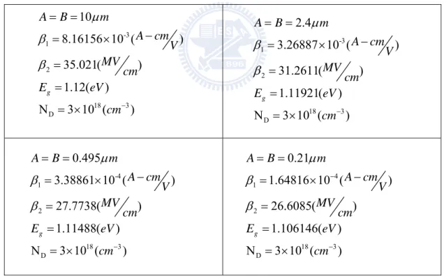
Fig. 4.8 Leakage currents in off-state nMOSFETs for gate, drain, and bulk are shown, and the gate-to-STI spacing A=B=a=10μm for no stress. ··· 56
Fig. 4.9 Leakage currents in off-state nMOSFETs for gate, drain, and bulk are shown, and the gate-to-STI spacing A=B=a=2.4μm for stress about -20 MPa. ··· 56
Fig. 4.10 Leakage currents in off-state nMOSFETs for gate, drain, and bulk are shown, and the gate-to-STI spacing A=B=a=0.495μm for stress about -125 MPa. ··· 57
Fig. 4.11 Leakage currents in off-state nMOSFETs for gate, drain, and bulk are shown, and the gate-to-STI spacing A=B=a=0.21μm for stress about -320 MPa. ··· 57
Fig. 4.12 The substrate hole current under mechanical stress which can be found to be made up of the surface BTBT (band-to-band tunneling or GIDL), gate-to-substrate tunneling, and bulk BTBT in the different VDG. The GIDL is about in 2V< VDG<3V
Fig. 4.13 GIDL (or surface BTBT) current under different gate-to-STI sidewall spacing values. ··· 59
Fig. 4.14 (a) The electric field is linearly distributed across the tunneling barrier in the X direction (See Fig. 4.14(b)) provided the lateral field is suppressed. ··· 60
(b) Device cross sections. The top one is a non-LDD device and the bottom one is a full-overlap LDD device. The lateral field is suppressed by increasing the phosphorus doping. The total field is the vector sum of the vertical field and the lateral field. ··· 61
Fig. 4.15 The electric field with model’s calculation and TRP. GIDL happened in 2V<VDG<3V. ··· 62
Fig. 4.16 (a) Energy band diagram based on the previous model. The value of band bending is fixed at 1.2 V. The band-to-band tunneling occurs only at the Si-Si02 interface. ··· 63
(b) Energy band diagram based on the new model. The value of band bending
(Vbend) creases over 1.2 V. The band-to-band tunneling occurs in the shaded area.
··· 63 (c) Cross-sectional view of a planar nMOSFET, as indicated in the electric field
direction. ··· 64
Fig. 4.17 The electric field in the oxide under different STI-induced stress. However, they are very close. ··· 65
XI
Fig. 4.18 The electric field in silicon under different STI-induced stress can be transferred
from the electric field in the oxide. ··· 65
Fig. 4.19 The band bending voltages are compared in the model’s calculation and TRP’s simulation. ··· 66
Fig. 4.20 The band bending voltages under STI-induced mechanical stress. ··· 66
Fig. 4.21 Energy gap barrier versus gate-to-STI sidewall spacing. ··· 67
Fig. 4.22 Using conventional GIDL region in the new modelcalculation. ··· 68
Fig. 4.23 Conventional GIDL in off-state (VG<0V). ··· 68
Fig. 4.24 (a) Applying advanced current model to fit the measurement data (2V<VDG<3V).69 (b) Using the TRP’s parameters to simulate the GIDL under mechanical stress (2V<VDG<3V). ··· 70
Fig. 4.25 Calculation flow chart ··· 71
Fig. 4.26 (a)The effective tunneling area under the GIDL dependence on STI-induced mechanical stress (a=10μm). ··· 72
(b)The effective tunneling area under the GIDL dependence on STI-induced mechanical stress (a=2.4μm). ··· 72
(c)The effective tunneling area under the GIDL dependence on STI-induced mechanical stress (a=0.495μm). ··· 73
(d) The effective tunneling area under the GIDL dependence on STI-induced mechanical stress (a=2.4μm) ··· 73
Fig. 4.27 (a) Conventional GIDL model in comparison with the advanced GIDL model via TRP (a=10μm). ··· 74
(b) Conventional GIDL model in comparison with the advanced GIDL model via TRP (a=0.21μm). ··· 74
Table 1 Different bias conditions. ··· 75
‐ 1 ‐
Chapter 1
Introduction
Section 1.1 General Introduction
In order to shrink MOSFET devices into the deep sub-micrometer regime, the level of channel dopants will increase inevitably and the gate dielectric thickness must decrease. This leads to a significant increase of the normal electric field, imposing high demands on the advanced technology and on the understanding of the device physics involved. Thus, accurate characterization and modeling of ultra thin oxides in the leakage current in the high field conditions is essential and crucial [1]. A series of models including the tunneling regime have recently been published concerning the electron direct tunneling in n+ poly-gate nMOSFETs and the electron tunneling from the valence band into the conduction band in the gate-to-drain overlap region.
Recently, the mechanical stress induced by shallow trench isolation (STI) attracts a lot of attention [2]. Both the experimental work and numerical simulation have demonstrated that the STI stress magnitude is rather high in scaled MOSFETs [3, 4]. The effect of the STI-induced stress on the carrier mobility has been discussed in [5]. The enhancement or suppression of dopant diffusion due to STI-induced stress is also reported in [6].
Moreover, the leakage currents at high electric field are not only the single factor induced by the only one mechanism [1], but also have the mechanical stress induced variation [2]. In this thesis, the mechanical stress induced by shallow trench isolation (STI) significantly affects the device behavior in the advanced CMOS technology.
The thesis presents that the stress induced from the STI spacing sidewall can be extracted by the basis of the triangular potential approximation [7].
The electrical approach to the local mechanical stress around the source/drain extension corner of uniaxially stressed nMOSFETs is also presented later. With the proper measurement, we can separate correctly the dominated leakage current mechanism in the off-state regime. Therefore, the edge direct tunneling current in the n+ poly-gate and the gate-induced drain leakage at high electrical field in the gate-to-drain overlapped region can be simulated from the triangular potential simulator. Thus, the parameters from the current mechanism can be extracted reasonably.
Section 1.2 Organization of The Thesis
In this thesis, it is organized based on the following arrangement. Chapter 2 discusses the techniques of the stress extracted from the gate-to-STI (shallow trench isolation) spacing sidewall for ultrathin gate oxide nMOSFETs. Through the TRP (triangular potential) simulator, the STI-induced stress can be extracted and the quantum confinement phenomenon is depicted in the subbands in nMOSFETs.
In Chapter 3, on the one hand, the stress-induced leakage current variation is investigated, and the edge direct tunneling (EDT) currents reflect the STI-induced stress. On the other hand, the EDT of electrons from n+ plysilicon to underlying n-type drain extension in off-state nMOSFETs can be simulated via TRP. Moreover, it is in agreement with the measured data under the stress condition resulted from the STI. Applying the correct model, the EDT under the stress condition can reveal the effective tunneling path of EDT with the doping concentration of drain extension
‐ 3 ‐
taken into account.
In Chapter 4, under off-state situation, the drain leakage results from the edge direct tunneling (EDT) rather than conventionally gate-induced drain leakage (GIDL) or bulk band-to-band tunneling (BTBT). However, the conventional GIDL (or surface BTBT) is recognized as the major drain leakage in off-state, but from our experiment, the leakage current is dominated by the different magnitude of the drain to gate voltage. They can be separated through this experiment, and fitted by the proper model. Especially, in high electric field, the dominated leakage is the GIDL and it is influenced by the stress. Thus, the energy gap and band bending voltage vary and are not always constant. In addition, using the TRP, the simulated data can be calculated in the adequate model. The parameters can be extracted subsequently.
Finally, conclusions are given in Chapter 5, where the major contribution of the work is proposed.
Chapter 2
Stress Extraction
Section 2.1 Device Under Study
The n+ poly-silicon gate n-MOSFETs were fabricated in a state-of-the-art manufacturing process. The device process flow is depicted in Fig. 2.1. Three key process parameters obtained by the capacitance-voltage (C-V) fitting are as follows: n+ poly-silicon doping concentration = 1 10 cm× 20 −3, gate oxide thickness = 1.27 nm ,
and substrate doping concentration = 4 10 cm× 17 −3. In this chapter, the devices was
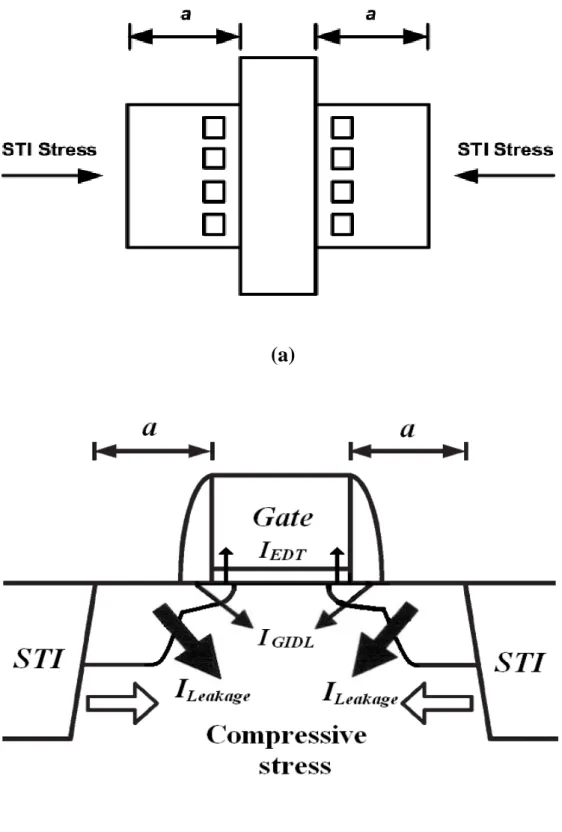
characterized, for gate length L of 1 mμ , and gate width W of 10 mμ . For the devices, the gate length along the 110 direction was 1 mμ large enough that the following effects can be effectively eliminated: external series resistance and short channel or drain induced barrier lowering (DIBL), whereas the gate width was 10 mμ , indicating that the transverse stress is relatively negligible. The layout technique was utilized in terms of gate edge to STI (Shallow Trench Isolation) sidewall spacing, which is designated as a , with four values of 10, 2.4, 0.495, and 0.21 mμ . A decrease in a means increased magnitude of longitudinal stress. The schematic cross section and the topside view of the test device are depicted in Fig. 2.2(a) and (b).
A considerable number of contacts were formed on the source/drain diffusion along the gate width direction, far away from the STI in 110 direction. The spacing between the gated edge is fixed in this work. It has been reported that silicide can introduce stress into channel and its effect can be eliminated by well controlling the
‐ 5 ‐
silicide formation [5]. Thus, the silicide process was fine tuned for the device under study to minimize its effect as compared with STI stress.
The gate direct tunneling current was measured in inversion conditions with the source, drain, and substrate all tied to ground. Also characterized was mobility on the same device at VD = 25mV. The change of the conduction-band electron direct
tunneling current at VG=1V and the mobility at VG=0.5V, all with respect to A = 10
μm , are plotted in Fig. 2.3 versus gate to STI spacing. It can be seen that a decrease in the gate to STI spacing can produce an increase in both the gate current and threshold voltage while degrading the mobility [9].
Section 2.2 The TRP simulator
The TRP simulator was constructed to quantify the direct tunneling current density on the basis of the triangular potential approximation in the channel, taking into account the poly-silicon depletion [7]. A good starting point to understand the band splitting induced by strain or stress is from the aspect of broken symmetry. Due to the commutation between operations and crystal Hamiltonian, symmetry plays a vital role in determining the band structure. Compressive stress causes the repopulation of the electrons, decreasing the electron density and Si/ SiO2barrier height in theΔ valley, 2 while increasing the electron density and Si/ SiO2barrier height in theΔ valley [10]. 4 Note from the expression listed above that the change in the conduction band energy may cause the strain altered gate leakage (Fig. 2.4).
ellipsoids of constant electron energy in reciprocal space, each corresponding to one of the degenerate conduction band valleys. In this thesis, quantum confinement and stress both enhance the degeneracy between the four in-plane valleys (Δ ) and the 4 two out-of- plane valleys (Δ ) owing to energy splitting. Compressive stress 2 decreases the electron population in theΔ valley due to a higher out-of-plane mass 2 and a significantly longer lifetime compared to theΔ valley, resulting in an increased 4 electron tunneling current [11].
The electron direct tunneling current density can be modeled by the TRP simulator. First of all, the potential drop due to poly depletion is determined through the following expression [9]:V εox2 Fox2 2qεsiNpoly
poly = , and the substrate band bending
can be written as Vs = VG −VFB −Vpoly−Vox , where V is the applied gate G
voltage,V the flat band voltage , FB V the oxide potential drop, andox Vpoly the potential drop in the n+ poly-silicon region. The reference point of this model is the conduction band edge of the Δ subband. Therefore, the tunneling barrier at the 4 cathode-side interface and the relative positions of the Δ and 2 Δ subbands can be 4 defined as [12]: 4 BC BC(stressed)=φ (unstressed)−Ed φ (2.1) 4 2 2 2(stressed) E (unstressed) Ed Ed EΔ = Δ + − (2.2) ) ( ) ( 4 4 stressed E unstressed EΔ = Δ (2.3) where 3.15eV ) ( BC unstressed = φ (2.4)
‐ 7 ‐
(
)( )
(
)( )
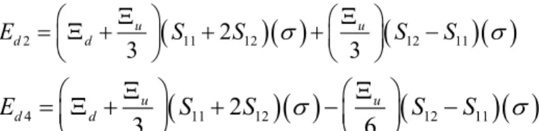
2 3u 11 2 12 3u 12 11 d d E = Ξ +⎜⎛ Ξ ⎟⎞ S + S σ +⎛⎜Ξ ⎞⎟ S −S σ ⎝ ⎠ ⎝ ⎠ (2.5)(
)( )
(
)( )
4 11 2 12 12 11 3 6 u u d d E = Ξ +⎜⎛ Ξ ⎟⎞ S + S σ −⎛⎜Ξ ⎞⎟ S −S σ ⎝ ⎠ ⎝ ⎠ (2.6) The change in the energy bandgap is then considered:(
)
( ) 1 4g g V d
E stressed =E unstressed + ΔE + ΔE (2.7)
Fig. 2.6 presents the band diagram when the cathode side is stressed, whereas no stress is applied on the cathode-side. Taking into consideration that the n+ poly-silicon region is also stressed, as depicted in Fig. 2.7, the electron group velocity normal to the interface in the anode-side should also be modified. By modeling the energy band as parabolic one, we can compare the relative energy shifts on both sides of the silicon oxide to derive electron group velocity normal to the interface on both the anode and cathode sides. The modifications in the following expressions alter the correction factors in our TRP simulator and thus change the transmission probability [12].
The normal components of electron group velocity on both the anode and cathode sides are listed below:
(
)
(
)
Z su m cath E cath 2 VSi = ,( )
( )
Z su m An E An 2 VSi = (2.8) where Esi(
Cath)
=(
EΔ2(unstressed)−(
ΔEd2 −ΔEd4)
)
(2.9)( )
(
(
d d)
)
d d ox si An E unstressed E E ⎜⎝⎛ E E ⎟⎠⎞+qV ′ Δ − Δ + Δ − Δ − = Δ2( ) 2 4 2 2 E (2.10) 0 91 . 0 m mZ = for Δ valley 2 (2.11)
(
) (
( ))
Esi Cath = EΔ4 unstressed (2.12)( ) (
)
d d ox si An = EΔ4(unstressed) +⎛⎜⎝ΔE 4 −ΔE 4′⎟⎞⎠+qV E (2.13) 0 19 . 0 m mZ = for Δ valley 4 (2.14)the primed and unprimed symbols represent the energy shift in the n+ poly-silicon region and the underlying substrate region, respectively.
It is now a straightforward task to calculate the electron direct tunneling current density. If all the subband energy levels are determined, then the inversion-layer carrier density per unit area can be expressed as [9, 12-15]
(
)
(
)
(
E E K T)
m g T K N B i di f i B i ⎟ + − ⎠ ⎞ ⎜ ⎝ ⎛ = 2 ln1 exp hπ , where the subscript
idenotesΔ and2 Δ , 4 KBT is the thermal energy, giis the degeneracy of the valley,
and mdiis the density of state effect mass. Then, by relating the boundary conditions between the oxide and silicon surface, the charge conservation relationship
(
NS Ndepl)
oxFoxq + ≈ε [7, 9] can be established. From now on, it is the TRP simulator that employs an iteration procedure to select the appropriate oxide field value to meet the above expression. The flowchart of the TRP simulator is drawn in Fig. 2.8.
Section 2.3 Stress Extraction via TRP simulator
Existing direct tunneling models [16, 17] on the basis of the triangular potential approximation [7] in the channel, which takes into account the poly-silicon depletion, can be readily applied with some slight modifications such as incorporating stress dependencies of the subbands. The electrons in inversion primarily populate the two
‐ 9 ‐
lowest subbands [15]: one of the twofold valley Δ2 and one of the fourfold valley Δ4.The corresponding stress dependencies are well defined in the literature [15, 18-19].
(
)( )
(
)( )
2 3 , 2 2 * 11 12 12 11 2 9 2 3 3 16 2 eff u u d hqE E S S S S m σ σ Δ Δ Δ ⎛ ⎞ ⎛ Ξ ⎞ ⎛Ξ ⎞ ⎜ ⎟ = + Ξ +⎜ ⎟ + +⎜ ⎟ − ⎜ ⎟ ⎝ ⎠ ⎝ ⎠ ⎝ ⎠ (2.15)(
)( )
(
)( )
2 3 , 4 4 * 11 12 12 11 4 9 2 3 6 16 2 eff u u d hqE E S S S S m σ σ Δ Δ Δ ⎛ ⎞ ⎛ Ξ ⎞ ⎛Ξ ⎞ ⎜ ⎟ = + Ξ +⎜ ⎟ + −⎜ ⎟ − ⎜ ⎟ ⎝ ⎠ ⎝ ⎠ ⎝ ⎠ (2.16)where EΔ2and EΔ4denote the energy levels for theΔ2andΔ4valley respectively, the quantization effective masses are m* 0.92mo
2 =
Δ and m 0.19mo
* 4 =
Δ , and the elastic
compliance constants are S 12
(
m2 N)
11 7.68 10 − × = and S 12(
m2 N)
12 2.14 10 − × − = .The hydrostatic and shear deformation potential constants Ξd =1.13eV and
eV
u =9.16
Ξ , which are close to those of Ref.[15], [20] were cited here. Stress along 110 direction can be resolved into two different components normal and shear stress terms in 110 coordination. Shear terms can cause the band distortion, which in turn influences the effective mass. This effect becomes significant when applied strain approaches 1% and beyond, whose magnitude is much greater than that in our study case. Thus, it is reasonable to assume that effective mass change can be neglected under moderate stress in the subsequent calculation. One of the expressions for the effective electric field Eeff can be found elsewhere [15]. With the
aforementioned process parameters as input, the two lowest subband levels with respect to the Fermi level Ef can be determined. The stress dependencies of the
in earlier works [15]. The inversion-layer carrier density per unit area can further be calculated by N KBT gimdi
(
(
(
Ef Ei)
KBT)
)
i ⎟ + − ⎠ ⎞ ⎜ ⎝ ⎛ = 2 ln1 exp h π [7], [16], where thesubscript i denotes Δ2 or Δ4, kBT is the thermal energy, g is the degeneracy of the i
valley, and mdi is the density of state effective mass. It is then a straightforward task to
calculate the Wentzel–Kramers–Brillouin tunneling probability, taking into account the corrections for reflections from the potential discontinuities [12]. Here, the electron effective mass in the oxide for the parabolic-type dispersion relationship was used with mox ∼ 0.50 m0, which is equivalent to mox = 0.53m0 for the tunneling
electrons in the oxide using the Franz-type dispersion relationship [21]. The SiO2/Si
interface barrier height in the absence of stress is 3.15 eV.
Consequently, without adjusting any parameter, the conduction band electron direct tunneling current density can be calculated as a function of stress σ [15] as
( )
2( )
( )
4( )
( )
2 4 g qN qN J σ σ σ τΔΔ σ τΔΔ σ = + (2.17)The tunneling lifetime in (3) can be related to the transmission probability T as
2( ) /(T 2( )E 2( ))
τ σΔ = hπ Δ σ Δ σ and τ σΔ4( )= hπ /(TΔ4( )σ EΔ4( ))σ .
With the above approach, we found that the uniaxial channel stress of around 0, −20, −125, and −320 MPa for a gate-to-STI spacing of 10, 2.4, 0.495, and 0.21 mμ , respectively, can reproduce gate direct tunneling current versus gate voltage characteristics. The corresponding gate current change is plotted in Fig. 2.3 versus the extracted channel stress with gate voltage as a parameter. It can be seen that the magnitude of the gate current change increases linearly with the stress, which is
‐ 11 ‐
consistent with those published elsewhere [15]. Again, in agreement with the citation [15], the slope of the straight line in Fig. 2.3 increases with decreasing gate voltage. This trend clearly points out that the accuracy of the proposed method can be enhanced by lowering gate voltages.
Chapter 3
Edge Direct Tunneling Leakage Current Simulated
with TRP
Section 3.1 Introduction
The off-state drain leakage is one of the big issues for aggressively shrunk MOSFET’s. The well recognized mechanisms are the gate-induced-drain-leakage (GIDL or surface band-to-band tunneling) [22], [23], the bulk band-to-band tunneling (BTBT) [24], and the drain-induced-barrier-lowering (DIBL) enhanced subthreshold conduction. In the case of reverse substrate bias for suppression of DIBL or subthreshold leakage, the bulk BTBT dominates [25]. On the other hand, the gate leakage due to direct tunneling (DT) [26] was measured per unit oxide area and a certain criterion of 1 A/cm set the ultimate limit of scalable oxide thicknesses [27], [28]. Recently, Yang et al. [29] have originally explored a dominant off-state leakage component via edge direct tunneling (EDT) of electron from n poly-silicon to underlying n-type drain extension. Also carried out in [29] is the I-V modeling obtained by following the procedure in [12], [16]. However, some parameters of great relevance were not clarified yet, such as the tunneling path area and the doping concentration of drain extension. In particular, the oxide field is an essential input parameter to the DT I-V model in [12]. We report that as scaled gate oxide thickness approaches the DT regime, the EDT of electron from n poly-silicon to underlying n-type drain not only dominates the gate leakage, but also can prevail over the conventional GIDL (Fig. 3.1), in agreement with [29]. This phenomenon is more pronounced for thinner oxide thicknesses, and EDT can even compete over the bulk
‐ 13 ‐
BTBT in the case of reverse substrate bias not mentioned in [29]. It is clarified that the gate leakage in stand-by mode indeed originates from the edge part rather than the whole gate oxide, and thus should be measured per unit gate width rather than per unit oxide area as in [27], [28]. Also presented is a physical model for the first time derived for the oxide field at the gate edge by accounting for electron subband in the quantized accumulation poly-silicon surface and its band diagram can be seen in Fig. 3.2. This model is valuable in enabling consistently the reproduction of EDT I–V, the extraction of EDT path size (Fig. 3.3), and doping concentration of drain extension.
Section 3.2 Experiment and Characterization
The test device was an n+ poly-silicon gate n-MOSFET as fabricated in a state-of-the-art manufacturing process. The device process flow is depicted in Fig. 2.1. Also plotted in the figure is the schematic topside view of the test device. Three key process parameters were obtained by capacitance–voltage (C–V) fitting: n+ poly-silicon doping concentration =1 10 cm× 20 −3, gate oxide thickness =1.27 nm , and
substrate doping concentration=4 10 cm× 17 −3 . In this process, the shallow-trench
isolation (STI)-induced compressive stress was applied. A layout technique was utilized to produce a variety of stress in terms of the gate edge to STI sidewall spacing, designated as a, with four values of 10, 2.4, 0.495, and 0.21 μm. A decrease in a means increased magnitude of longitudinal stress. Considerable numbers of contacts were formed on the source/drain diffusion along the gate width direction, far away from the STI in the 110 direction. The spacing between the diffusion contact and the gate edge is fixed in this paper. With the source, drain, and substrate all tied to ground (in Table. 1 Bias condition (2)), the measured valence-band electron tunneling current in inversion (for the gate voltage VG larger than the threshold voltage Vth ) or
equivalently the substrate hole current was found to be unchanged, regardless of the stress. This indicates that the gate oxide thickness under study remains constant. The
I-V curves are shown in the following Fig. 3.4 and 3.5.
Section 3.3 Physical Model for EDT
The electron direct tunneling from the accumulated poly-silicon surface down to the underlying silicon was measured versus negatively biased gate voltage with the source, drain, and substrate all tied to the ground. It can be seen in Fig. 3.4 that the resulting substrate hole current, which essentially is equal to the electron gate-to-substrate tunneling current, increases with decreasing a. Such dependency reflects the increasing magnitude of lateral compressive stress in the poly-silicon. The confirmative evidence of this origin is that for a given gate-to-STI spacing, the corner stress and channel stress both are comparable, and since the tunnel oxide is rather thin, the lateral compressive stress at the surface of the poly-silicon is reasonably close to that of the underlying silicon. In contrast, the simultaneously measured source/drain or edge direct tunneling (EDT) current decreases with decreasing a, as shown in Fig. 3.5 and Fig. 3.6. To determine the underlying gate-to-source/drain extension overlap length where the EDT prevails, the existing edge direct tunneling models [1], [15], [17] on the basis of the triangular potential approximation [7] (Fig. 3.6) can readily apply with some slight modifications such as incorporating stress dependencies of the subbands in the accumulated poly-silicon surface. First of all, the oxide field Eox at the
gate edge is determined through the following expression:
DE ox poly FB DG V V V V V − = + + (3.1)
‐ 15 ‐
whereV is the applied gate voltage,DG V the flat band voltage, andFB V the oxide ox potential drop, tox is the gate oxide thickness, and Vpoly and VDE are the potential drops
in the n+ poly-silicon and source/drain extension region, respectively. The accumulated electrons mainly populate in the first subband E1 due to the lowest
quantized energy dominating. Then, relating the sheet charge density to the number of occupied subband states can establish the charge conservation relationship
1 2 ( ) d fn ox ox m q E E η ε E Q π − = = h (3.2)
where Efn is the quasi-Fermi level in n+ poly-gate, η is the degeneracy factor, and Q is
the available charge for tunnel process. The corresponding stress dependency of the quantized energy is well defined in the literature [9], [15].
(
)( )
(
)( )
2 3 1 11 12 12 11 9 ( ) 2 3 3 16 2 ox ox u u d Si z hq E E S S S S m ε σ σ σ ε ⎛ ⎞ ⎛ Ξ ⎞ ⎛Ξ ⎞ =⎜⎜ ⎟⎟ + Ξ +⎜ ⎟ + +⎜ ⎟ − ⎝ ⎠ ⎝ ⎠ ⎝ ⎠ (3.3)where the elastic compliance constants S 12
(
m2 N)
11 =7.68×10−andS 12
(
m2 N)
12 =−2.14×10− . The hydrostatic and shear deformation potential
constants Ξd =1.13eV
and Ξu =9.16eV, [20], close to those of [15], were cited
here. With the aforementioned parameters as input, the lowest subband level with respect to the Fermi level can be quantified. Employing the lowest subband approximation to the accumulated n+ poly-gate and the deep depletion approximation to the source/drain extension region, as drawn in Fig. 3.6, the following expressions can, therefore, be derived:
2 1 2 / poly FN ox ox d E V E q E q m q π ε η ≈ = h + (3.4)
2 2 2 ox ox DE Si DE E V q N ε ε = (3.5)
where NDE is the doping concentration of the source/drain extension. Here, the
quantization effective masses mz = 0.98 m0 and md = 0.19m0, and η = 2 were adopted
to approximate the band structure for 110 oriented poly-silicon grain [12]. Then, it is a straightforward task to calculate the WKB tunneling probability, taking into account the corrections for reflections from the potential discontinuities [12]. Here, the electron effective mass in the oxide for the Franz-type dispersion relationship was used with mox = 0.53 m0. The SiO2 /Si interface barrier height in the absence of stress
is 3.15 eV. Consequently, the edge electron direct tunneling current density can be calculated as a function of the stress σ
( )
( )
EDT 1 TN Q I σ WL τ σ = (3.6)where W is the channel width, and LTN is the gate-to source/drain-extension overlap
length. The tunneling lifetime in this equation can be connected with the transmission probability T : τ π1 = h
(
T1( ) ( )
σ E1 σ)
.
Then, with known process parameters and published deformation potential constants [20] as input, the measured EDT was reproduced well, as displayed in Fig. 3.5. Electron tunneling onto the forbidden silicon bandgap occurs in −0.1 V < VG < 0
V; however, an appreciable gate current was measured there. This indicates the existence of the oxide traps or interface states. Only at a more negatively biased gate voltage where the EDT dominates can the effect of the traps be alleviated. In addition, it was found experimentally that the gate edge direct tunneling current is several orders of magnitude larger than the gate-to-substrate current, and hence is dominant
‐ 17 ‐
spans a range of 6.1, 6.0, 5.7, and 5.0 nm for a of 10, 2.4, 0.495, and 0.21 μm, respectively, as demonstrated in Fig. 3.7. The LTN values are found to be comparable
with those in the literature [1], [14], [17]. The shift of around 1.1 nm, caused by retarded doping lateral diffusion for stress change from 0 to −320 MPa, is reasonable with respect to the process simulation [6]. In the cited work [6], a device/process-coupled simulation was carried out to produce the lateral doping profile from the source through the channel to the drain, with and without the strain dependencies.
Chapter 4
Gate Induced Drain Leakage Current Simulated
under STI-Induced Stress
Section 4.1 Introduction
This drain leakage current is caused by the gate-induced high electric field in the gate-to-drain overlap region. Many researchers have attributed the leakage current to the band-to-band tunneling occurring in the overlap region and named the phenomenon gate-induced drain leakage current (GIDL). The extracted oxide thickness, potential, and doping profiles in the gate-to-drain overlap region are found to play important roles in the GIDL current. The GIDL and its degradation have restricted the scaling of oxide thickness and power supply voltage. In addition, the band-to-band tunneling induced hot-electron injection is proposed to be a programming method for flash memory cells [30] and an erase operation for EEPROM memory cells [31].
Some band-to-band tunneling current models for the GIDL have been proposed [23], [32-35]. These models show well-accepted physical dependence. However, the model in [23] and [32] ignores two physical parameters dependence. The most noticeable parameter is the lateral electrical field near the drain-to-gate overlap region. The other parameter that should be considered is the dependence of the band bending on the drain doping concentration. The model in [34] considers the built-in lateral field caused by the lateral gradient of the drain doping concentration, but it neglects the contribution of the external drain voltage to the lateral field. The model in [35]
‐ 19 ‐
and lateral field, but the model is a complex integral-form equation. However, the mechanical stress induced by shallow trench isolation (STI) influences the electrical characteristics of the device, including the EDT and GIDL tunneling currents in Fig. 4.1.
Section 4.2 GIDL Dependence on STI-Induced Mechanical Stress
In this chapter, we concentrate on the STI stress effect on gate-induced drain leakage (GIDL) current [22], [23]. The physical mechanisms for enhancing the GIDL due to the STI-induced stress are investigated. As design rules or layout dimensions are scaled down, the high-stress region encroaches further into the channel region. The GIDL dependence on layout parameters will also be discussed.
This work focuses on the residual STI-stress after processing. Fig. 4.1 schematically shows the top view of simulated n-MOSFET device as well as its cross section along the channel direction. Three key layout parameters are defined: channel width W, gate length L, and active-area lengths a(the length from the gate center to the STI inner edges as illustrated in Fig. 4.l (b)).The symmetry between the source and drain will be discussed to treat the EDT and GIDL under the STI-induced stress condition. In simulations the channel width is chosen as 10μmto avoid narrow width effects. The gate drain overlap is kept at 0.05μm. The other important bias parameters are summarized in Table 1.
Previous experiment and numerical simulation have proved that STI-stress has a peak around the STI inner edges and rapidly decays from the edges to the channel region [2]. When approaching to the channel region, the stress variation is not drastic.
Since the GIDL takes place in this region, the stress in the simulation could be treated as constant value for simplicity. Based on the data in [2], the uniform STI-stress is implemented according to the changes of a.
In order to physically analyze the stress effect on GIDL current, it is desirable to distinguish their contributions to the GIDL current separately. In Fig. 3.1, the leakage current components can be found from Yang, et al. [1]:
IG=Igb + IEDT
ID=IEDT + IGIDL+ Ibulk-BTBT
IB= Igb + IGIDL + Ibulk-BTBT
where IG, ID, and IB are the gate current, drain current, and bulk current, respectively,
and then Igb is the gate-to-substrate tunneling current, IEDT is the edge direct tunneling
current, IGIDL is the gate-induced drain leakage current, and Ibulk-BTBT is the bulk
band-to-band tunneling current.
Direct tunneling current from the gate overlap region into the underlying source/drain extension region (also identified in current literature as edge direct tunneling or EDT) has been recognized as the principal source of off-state power dissipation in state-of-the-art VLSI chips and the measured data versus the simulated line from the TRP in Fig. 4.2-4.5. Yang, et al. [1] have also shown that the components of gate leakage exceeds even band-to-band tunneling (BTBT) or gate-induced drain leakage (GIDL) for ultrathin gate oxide n-MOSFETs in Fig. 4.6-4.11 and their bias conditions are different as shown in Table. 1.
‐ 21 ‐
Section 4.3 Experiment and Characterization
The method for the stress-dependent GIDL simulation is as follows: Fig. 4.1(b) illustrates the tunneling leakage paths and related band diagrams (Fig. 4.16(a),(b)). With source open and under VG= -VD [1], the measured drain current, gate current,
and bulk current are plotted in Fig. 4.6 and Fig. 4.7 for two different gate widths. Fig. 4.8-4.11 all reveal that the drain current primarily comprises the GIDL, the bulk BTBT, and the gate current, implying the EDT as the origin of the latter component. It can be observed that the EDT dominates the gate leakage, and there exists a certain range where the EDT prevails over the conventional GIDL and bulk BTBT. This phenomenon is more pronounced for thinner oxide thicknesses. And then the GIDL can be separated adequately from the IB, bulk current by the measured method. In Fig.
4.8 for 1.27 nm thin oxide and STI a=10μm, the polarity of the bulk current is
reversed due to gate-to-substrate tunneling. Besides, we found experimentally that the EDT leakage is indeed proportional to the gate width, regardless of the aspect ratio (W/L). This means that the gate leakage in stand-by mode (i.e., only source and gate tied to ground) should be adequately measured per unit gate width in Fig. 4.2-4.5.
In Fig. 4.12, we found the GIDL (or surface BTBT), gate-to-substrate tunneling, and bulk BTBT in the substrate hole current from the corner. Thus, the GIDL can be shown in the high electric field region and the current model can be adapted in the proper regime in Fig. 4.13.
Section 4.4 Band-to-Band Tunneling Current Model
In this section, the concept of the previous model is explained and the inadequacy of this model is demonstrated. A number of have attributed subbreakdown to the
band-to-band tunneling process in silicon in the gate-to-drain overlap region, as illustrated in Fig. 4.16. The cross section shown in Fig. 4.16 is simply a gated-diode configuration. When high voltage is applied to the drain with the gate grounded, a deep-depletion region is formed underneath the gate-to-drain overlap region. Electron-hole pairs are generated by the tunneling of valence band electrons into the conduction band and are collected by the drain and substrate separately. Since all the minority carriers generated thermally or by band-to-band tunneling in the drain region flow to the substrate due to the lateral field, the deep-depletion region is always present and the band-to-band tunneling process can continue without creating an inversion layer. Band-to-band tunneling is possible only in the presence of a high electric field and when the band bending is larger than the energy band gap, Eg.
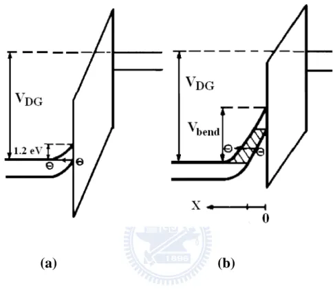
The conventional model has assumed that (a) the value of band bending in the depletion layer in the drain-to-gate overlap region is fixed at Eg=1.12 eV, which is the
minimum value necessary for a tunneling process to occur, and that (b) band-to-band tunneling occurs only at a point of the Si-SiO2 interface, as shown in Fig. 4.16.
A simple expression for the surface field ([23], [32]) at the dominant tunneling
point is: 1.12 3 DG Si OX V E T − = (4.1)
where ESi is the vertical electrical field at the silicon surface, 3 is the ratio of silicon
permittivity to oxide permittivity, and Tox, is the oxide thickness in the overlap region.
The theory for tunneling current predicts [32] that exp( ) BTBT Si Si B I AE E − = (4.2)
‐ 23 ‐
subbreakdown current on both the oxide thickness and the impurity distribution plays an important role in the subbreakdown phenomenon. Although the previous model took into account the effect of oxide thickness, the dependence on the impurity distribution was neglected. But, the calculated results do not agree with the experimental results, especially under the stressed condition. The simplified model is, therefore, totally inadequate for the subbreakdown phenomenon.
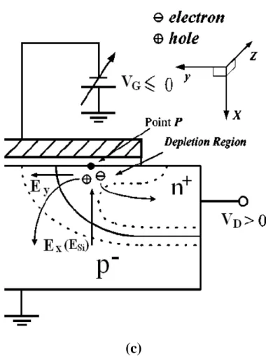
Fig. 4.16(c) shows a cross-sectional view of an n-MOSFET device. When the drain is connected to a positive bias and the gate is connected in the vicinity of zero bias or even to a negative bias, a depletion region is formed underneath the drain-to-gate overlap region and a high field is created in the depletion region. Electron-hole pairs are generated by the tunneling of valence band electrons into the conduction band and collected by the drain and substrate separately. In Fig. 4.14(a), a vertical and lateral energy band diagram is presented near the point, as shown in Fig. 4.14(b). In Fig. 4.14(b), the electrons tunnel into the drain due to the vertical field ESi is shown. For
the band-to-band tunneling process, because the tunneling electrons in the drain dominate the GIDL, the vertical field in the drain is the dominant field for the leakage and is an important parameter in the tunneling current model [36] in Fig. 4.15. In addition, the vertical field depends on the band bending Vbend, as shown in Fig.
4.16(b), and the Vbend is strongly related to the drain doping concentration. Therefore,
the drain doping concentration is also an important parameter in the tunneling current model. Thus, the vertical field in the overlap region could be estimated using depletion approximation.
When the VDG is a constant, the vertical fields in the gate-to-drain overlap region
gate voltage is more negative, the drain voltage must be more positive. The GIDL would not be equal under constant drain-to-gate voltage VDG. The GIDL is dependent
on both the drain-to-gate voltage VDG and drain voltage VD [33], [34].
In this section, the concept of the new accurate model is explained, and the new model is introduced in detail. The concept underlying the new model has four aspects: (a) a deep-depletion layer is created in silicon in the drain-to-gate overlap region and the value of band bending increases monotonically over 1.12 eV as a function of drain voltage.
(b) The dependence of subbreakdown on the impurity distribution is considered. (c) Both the electric field of the deep-depletion layer and the tunneling region are calculated by depletion approximation.
(d) The band-to-band tunneling rate is calculated by the two-band theory.
The concept for this model is given as follows. Holes are generated by band-to-band tunneling. However, an inversion layer is not formed in the drain-to-gate overlap region, because the generated holes flow into the substrate due to the lateral electric field. Therefore, the band bending value and the electric field increases monotonically as drain voltage increases in Fig. 4.17-4.20. The width of the depletion region where electron tunneling occurs also increases as the drain voltage increases. Both the electric field and the band bending value can be estimated by depletion approximation, as functions of the drain voltage, the distribution of impurity density in the drain, and the oxide thickness.
When the impurity distribution in the drain-to-gate overlap region is uniform, for example, the electric field in the depletion region becomes [33]
‐ 25 ‐ 2 (1 ) 2 Si bend D D Si Si D Si bend V qN qN E X qN V ε ε ε = − (4.3)
where Esi is the electric field in the depletion region, Vbend is the band bending value, ND is the impurity density in the drain region, q is the electron charge, εSi is dielectric constant of the silicon, and X is a coordinate normal to the Si-SiO2 interface.
The silicon surface is represented by the plane at X = 0 and the bulk by a positive value of X. From the Gaussian law, the continuity equation for electric displacement at the Si-SiO2 interface becomes
( 0) ( ) /
SiESi X oxEox ox VDG Vbend Tox
ε = =ε =ε − (4.4)
where EOXis the electric field in the SiO2 layer, and εox is the dielectric constant of
the oxide. Substituting (3) into (4), the band bending value is given as a function of drain voltage as follows:
2 2 2 2 2 ( 2 ) ( ) D ox Si D ox Si bend DG FB DG DG FB ox ox qN T qN T V V V ε V ε V V ε ε = − + − + − − (4.5)
When the gate electrode is biased negatively, the gate overlap region over the source/drain extension region immediately goes into accumulation given the fact that the flat band voltage between the heavily doped n+ poly-Si region and the source/drain extension region is almost zero.
2 2 2 2 2 ( 2 ) D ox Si D ox Si bend DG DG DG ox ox qN T qN T V V ε V ε V ε ε = + − + − (4.6)
Full-overlap LDD is used to study this tunneling leakage because the lateral field is suppressed while the drain concentration is high enough so that the dominant tunneling point has a band bending of 1.2 eV (Fig. 4.16(a), (b)). However, the energy gap decreases as the STI spacing wall a decreasing in Fig. 4.21. The proper and simple current model for GIDL (or surface BTBT) ([34], [36-38]) can be expressed as
follows: 2 1 exp( ) BTBT Si Si I E E
β
β
− = (4.7) 2 1 3 1 2 r g bend eff q m E V Area π β β = × × h (4.8) 1 3 2 2 2 2 2 r g m E q π β = h (4.9) where ( ) 2 D bend Si Si vertical Si qN VE =E = ε ; mr=0.2m0 is the effective mass[33], m0 is the
electron rest mass, h is the Plank’s constant divided by 2π, and Areaeff is the effective tunneling area. Therefore, using this simplified model, we can fit the measured GIDL under the stressed condition well.
Section 4.5 Results with Calculation and Simulation via TRP
In comparison with the conventional model, the energy gap and the band bending voltage that can be seen in the Fig. 4.19-4.21 are not always constant under the stressed condition. When a crystal is deformed by mechanical stress, the crystal symmetry and lattice spacing are altered and hence the energy bands change. The reasons to explain strain-induced band structure changes are the deformation potential theory proposed by Bardeen and Shockley [39]. The band shifts due to crystal deformations could be described by a perturbation of the local crystal potential. They concluded that the stress would narrow the silicon band gap.
The early experiment and simulation have proven that STI processing would induce compressive stress due to the swell of the STI wall volume [2]. So the induced negative strain tensor causes the energy gap Eg narrowing (Fig. 4.21). In Eqs.(4.6),
‐ 27 ‐
(4.7) and (4.8), except of Eg, the other parameters are kept constant under the
compressive stress. Thus GIDL is inevitably enhanced, which is verified by our experimental results as shown in Fig. 4.12 in the high electric field.
The energy gap decreases as the stress increasing from the TRP simulator, especially under the stressed condition, and the band bending voltage increases as the drain to gate voltage increasing. With calculation of the Esi and Vbend, the proper
region is chosen essentially, and then we define the GIDL region as the drain-to-gate voltage that is 2~3 volts [1] (Fig. 4.13). In addition, the leakage current in off-state cannot be in agreement with the GIDL current model, especially in the low electric field (Fig. 4.22 and 4.23). However, using the conventional model of GIDL captures the measured data well in Fig. 4.27. The electric field, energy gap, and band bending voltage of the calculation results compare well with the simulation of the TRP and they are very close in Fig. 4.15, 4.17, and 4.18. From this, the fitted line can be in agreement with the GIDL in the separated region under the stressed condition well in Fig. 4.24. Therefore, the parameters can be extracted from the fitted line in the Table. 2, and the effective tunneling area (Fig. 4.26) can also be extracted as well. The calculation flow chart is described as follows: Fig. 4.25. In addition, the extracted parameters, β1 and β2, decrease as the STI-induced stress increases. Moreover, the effective tunneling areas extracted from the different STI spacing sidewall decrease with increasing drain to gate voltage.
Chapter 5
Conclusion
The EDT (Edge Direct Tunneling) current decreases as the gate-to-STI spacing sidewall decreases. The Gate-Induced Drain Leakage (GIDL or surface BTBT) current increases as the gate-to-STI spacing sidewall decreases. The energy gap and the band bending voltage of the conventional model do not change as the stress increasing, and the GIDL (or surface BTBT) fitting lines do not agree with the measurement data well. The tunneling area decrease as the stress increasing, and the energy gap also decrease when the STI-wall decreases.
Using the BTBT current model to fit the conventional GIDL, the fitting line cannot agree with the ideal condition, so the proper region has to be chosen essentially. With the measured method from Yang’s et. al, the reasonable region can be separated clearly. So the current model can be agreement with the measured data, the region is chosen well.
Until now we have analyzed the STI-stress effects on GIDL from the weak to strong electric field. It is clear that the STI-stress reduction could ameliorate the GIDL enhancement. There are two methods to reduce the STI-stress magnitude. Although the new STI process such as STI-wall-oxide nitridation could reduce stress via the decreasing STI wall volume, this method is not maturated. Another effective method is the adoption of asymmetric layout. The STI-stress decreases rapidly with increasing active area lengths, i.e., a1 or a2, in a critical value (~2 mμ in Ref [3]).
‐ 29 ‐
Reference
[1] K. N. Yang, H. T. Huang, M. J. Chen, Y. M. Lin, M. C. Yu, S. M. Jang, D. C. H. Yu, and M. S. Liang, “Characterization and modeling of edge direct tunneling (EDT) leakage in ultrathin gate oxide MOSFETs,” IEEE Trans. Electron Devices, vol. 48, no. 6, pp. 1159–1164, Jun. 2001.
[2] M. Miyamoto, H. Ohta and Y. Kumagai et al., “Impact of reducing STI-Induced stress on layout dependence of MOSFET Characteristics,” IEEE Trans. Electron
Devices, vol. 51, pp. 440-443, Mar. 2004.
[3] V. Senez, T. Hoffmann and E. Robiliart et al., “Investigations of stress sensitivity of 0.12 CMOS technology using process modeling,” IEDM 2001, pp. 83 1-834.
[4] V. Senez, A. Armigliato and I. De Wolf et al., “Strain determination in silicon microstructrues by combined convergent beam electron diffraction, process simulation, and micro-Rama spectroscopy,” J. Appl. Phys., vol. 94, pp. 5574-5583, Nov. 2003.
[5] R. A. Bianchi, G. Bouche and 0. Roux dit Buisson, “Accurate modeling of trench isolation induced mechanical stress effect on MOSFET electrical performance,” IEDM 2002, pp. 117-120.
[6] Y. M. Sheu, S. J. Yang, and C. C. Chang et al., “Modeling mechanical stress effect on dopant diffusion in scaled MOSFETs,” IEEE Trans. Electron Devices, vol. 52, pp.30-38, Jan. 2005.
[7] H. H. Mueller and M. J. Schulz, “Simplified method to calculate the band bending and the subband energies in MOS capacitors,” IEEE Trans. Electron Devices, vol. 44, no. 9, pp. 1539–1543, Sep. 1997.
[8] Wenwei Yang, Guoxuan Qin, Xue Shao, Zhiping Yu, and Lilin Tian, “Analysis of GIDL Dependence on STI-induced Mechanical Stress,” in IEEE., 2005, pp. 769–772.
[9] Chen-Yu Hsieh, and Ming-Jer Chen, “Measurement of channel stress using gate direct tunneling current in uniaxially stressed n-MOSFETs,” IEEE Electron Device
Lett., vol. 28, no. 9, pp. 818–820, Sep. 2007.
[10] Y. Sun, G. Sun, S. Parthasarathy, S. E. Thompson, “Physics of process induced uniaxially strained Si,” Materials Science and Engineering B, Vol. 135, pp. 179-183, 2006.
[11] Scott E. Thompson, Guangyu Sun, Youn Sung Choi, and Toshikazu Nishida, “Uniaxial-Process-Induced Strain-Si: Extending the CMOS Roadmap,” IEEE Trans.
‐ 31 ‐
[12] Leonard F. Register, “Analytic model for direct tunneling current in polycrystalline silicon-gate metal-oxide-semiconductor devices,” Appl. Phys .
Lett.,Vol. 74 , No. 3 , January. 1999.
[13] I. Balslev, “Influence of uniaxial stress on the indirect absorption edge in silicon and germanium,” Phys. Rev., Vol. 143, No. 2, March. 1966.
[14] K. N. Yang, H. T. Huang, M. C. Chang, C. M. Chu, Y. S. Chen, M. J. Chen, “Model for hole direct tunneling current in P+ poly-gate pMOSFETs with ultrathin gate oxides,” IEEE Trans Electron Devices, Vol. 47, No. 11, November. 2000.
[15] Ji-Song Lim, Xiaodong Yang, Toshijazu Nishida, and Scott E. Thompson, “Measurement of conduction band deformation potential constants using gate direct tunneling current n-type metal oxide semiconductor field effect transistors under mechanical stress,” Appl. Phys. Lett., Vol. 89, pp.073509, 2006
[16] N. Yang, W. K. Henson, J. R. Hauser, and J. J. Wortman, “Modeling study of ultrathin gate oxides using direct tunneling current and capacitance–voltage measurements in MOS devices,” IEEE Trans. Electron Devices, vol. 46, no. 7, pp. 1464–1471, Jul. 1999.
[17] K. N. Yang, H. T. Huang, M. C. Chang, C. M. Chu, Y. S. Chen, M. J. Chen, Y. M. Lin, M. C. Yu, S. M. Jang, C. H. Yu, and M. S. Liang, “A physical model for hole direct tunneling current in p+ poly-gate pMOSFETs with ultrathin gate oxides,” IEEE
[18] C. Herring and E. Vogt, “Transport and deformation-potential theory for many-valley semiconductors with anisotropic scattering,” Phys. Rev., vol. 101, no. 3, pp. 944–961, Feb. 1956.
[19] C. G. Van de Walle and R. M. Martin, “Theoretical calculations of heterojunction discontinuities in the Si/Ge system,” Phys. Rev. B, Condens. Matter, vol. 34, no. 8, pp. 5621–5634, Oct. 1986.
[20] J. S. Lim, S. E. Thompson, and J. G. Fossum, “Comparison of thresholdvoltage shifts for uniaxial and biaxial tensile-stressed nMOSFETs,” IEEE Electron Device
Lett., vol. 25, no. 11, pp. 731–733, Nov. 2004.
[21] Z. A. Weinberg, “On tunneling in metal–oxide–silicon structures,” J. Appl.
Phys., vol. 53, no. 7, pp. 5052–5056, Jul. 1982.
[22] C. Chang and J. Lien, “Corner-field induced drain leakage in thin oxide MOSFETs,” in IEDM Tech. Dig., 1987, pp. 714–717.
[23] T. Y. Chan, J. Chen, P. K. Ko, and C. Hu, “The impact of gate-induced drain leakage current on MOSFET scaling,” in IEDM Tech. Dig., 1987, pp. 718–721.
[24] Y. Taur, D. A. Buchanan, W. Chen, D. J. Frank, K. E. Ismail, S. H. Lo, G. A. Sai-Halasz, R. G. Viswanathan, H.-J. C.Wann, S. J.Wind, and H. S. Wong, “CMOS scaling into the nanometer regime,” Proc. IEEE, vol. 85, pp. 486–504, 1997.
‐ 33 ‐
[25] M. J. Chen, H. T. Huang, C. S. Hou, and K. N. Yang, “Back-gate bias enhanced band-to-band tunneling leakage in scaled MOSFET’s,” IEEE Electron
Device Lett., vol. 19, pp. 134–136, 1998.
[26] H. S. Momose, M. Ono, T. Yoshitomi, T. Ohguro, S. Nakamura, M. Saito, and H. Iwai, “1.5 nm direct-tunneling gate oxide Si MOSFET’s,” IEEE Trans. Electron
Devices, vol. 43, pp. 1233–1242, 1996.
[27] S. H. Lo, D. A. Buchanan, Y. Taur, and W. Wang, “Quantum-mechanical modeling of electron tunneling current from the inversion layer of ultra-thin-oxide nMOSFET’s,” IEEE Electron Device Lett., vol. 18, pp. 209–211, 1997.
[28] G. Timp, K. K. Bourdelle, J. E. Bower, F. H. Baumann, T. Boone, R. Cirelli, K. Evans-Lutterodt, J. Garno, A. Ghetti, H. Gossmann, M. Green, D. Jacobson, Y. Kim, R. Kleiman, F. Klemens, A. Kornlit, C. Lochstampfor, W. Mansfield, S. Moccio, D. A. Muller, I. E. Ocola, M. I. O’Malley, J. Rosamilia, J. Sapjeta, P. Silverman, T. Sorsch, D. M. Tennant, W. Timp, and B. E. Weir, “Process toward 10 nm CMOS devices,” in IEDM Tech. Dig., 1998, pp. 615–618.
[29] N. Yang, W. K. Henson, and J. J. Wortman, “Analysis of tunneling currents and reliability of NMOSFET’s with sub-2 nm gate oxides,” in IEDM Tech. Dig., 1999, pp. 453–456.