國 立 交 通 大 學
材 料 科 學 及 工 程 學 系
博士論文
零維暨一維奈米材料之光電磁特性及結構研究
Structure Development, Optoelectronic and Magnetic
Characteristics of Zero- and One-Dimensional
Nanoscaled Materials
研究生:林士欽
指導教授:陳三元教授
Structure Development, Optoelectronic and Magnetic Characteristics of Zero- and One-Dimensional Nanoscaled Materials
Student: Shihchin Lin Advisor: Prof. Dr. San-Yuan Chen Department of Material Science and Engineering
National Chiao Tung University
Abstract
Material with nanometer-scale size have large ratio of surface to bulk atoms. Large surface always gives high active behavior and changes in both physical and chemical properties. Nanomaterials such as nanoparticles, nanotubes, nanorods and nanowires having size generally smaller than 100nm exhibit superior photoelectronic and magnetic properties in various applications. Therefore, in this thesis, the studies will be focused on the synthesis, structure analysis and property characterization of zero-/one dimensional nanoscaled materials.
In chapter 2, ZrO2, TiO2, ZnO and Al2O3, were chosen as raw materials to
synthesize a target for laser ablation. The formed nanoparticles exhibit two kinds of particle size distribution with 7~15 nm (70~90%) and 40~100 nm (10~30%). Nanoparticles synthesized at lower fluence laser ablation are rich in Zn composition and show more narrow distribution. While increasing laser fluence, the composition of the collected nanoparticles is primarily composed of Zr. A model based on composition and morphology of both nanoparticles and target with changing laser fluence was proposed to explain the phase evolution of nanoparticles. The average far-infrared emissivity of the nanoparticles based on ZrTiO4--ZnAl2O4 system is
measured to be more than 80﹪(wavelength range from 4 to 12 µm) and varies with crystal phase ratio.
alkaline solution. Nearly all of the dimethy-blue target pollutant at high concentration was removed when the photoreaction was performed in a short period. This novel nano TiO2 photocatalyst exhibits excellent photocatalytic activity because
it is well dispersed. Since no dispersant or organic binder was used, this synthetic process has the advantages of low cost and convenience.
In chapter 4, One-dimensional nanotube arrays of nickel-phosphate have been developed by electroless deposition into sub-micro to nanometer sized pores of the porous alumina templates. The dimension of the formed nanotubes has 1μm in length, 200~300nm in diameter and 80~150nm in thickness of tube walls. Transmission electron microscopy examination of the nanotubes clearly show amorphous hallow structure with a average grain size of ~5 nm. The hysteresis loops of the nanotube arrays show a coercive field of about 200Oe under treatment in 95%N2/5%H2 atmosphere at 500 oC as the magnetic field was applied along parallel
and perpendicular to tube axis. The nanotube arrays also exhibit an anisotropic magnetic property with easier saturation along the perpendicular direction. However, both coercive field and saturation of remanent magnetization of the nanotube arrays become lower while continually increasing heat treatment temperature up to 900oC.
In chapter 5, ordered silver- nickel core-shell nanowire arrays were successfully fabricated by electrodeposition. The ordered silver nanowire arrays embedded in a porous alumina template were first fabricated from an aqueous solution of Ag(NO3)2
and Ac(NH3). After removing out the template, the obtained silver nanowire arrays
were subsequently electrodeposited with nickel at 1.6~2.6V and 60oC using the electrolyte composed of NiSO4, NiCl2 and H3BO3. Transmission electron microscopy
(TEM) observation reveals that a 15 nm thick nickel film was coated on the surface of the silver nanowires with about 200 nm in diameter. It was found that the silver nanowires with nickel coating showed enhanced magnetic properties in comparison to
that of pure silver nanowires. The Magnetic Force Microscope (MFM) image of silver- nickel core-shell nanowires exhibits magnetic domain state. In addition, the hysteresis loops of the silver-nickel nanowire arrays show a coercive field of 180Oe, almost independent of the applied magnetic field parallel and perpendicular to nanowires. However, it was observed that a larger magnetic domain was found in parallel direction than that in perpendicular direction.
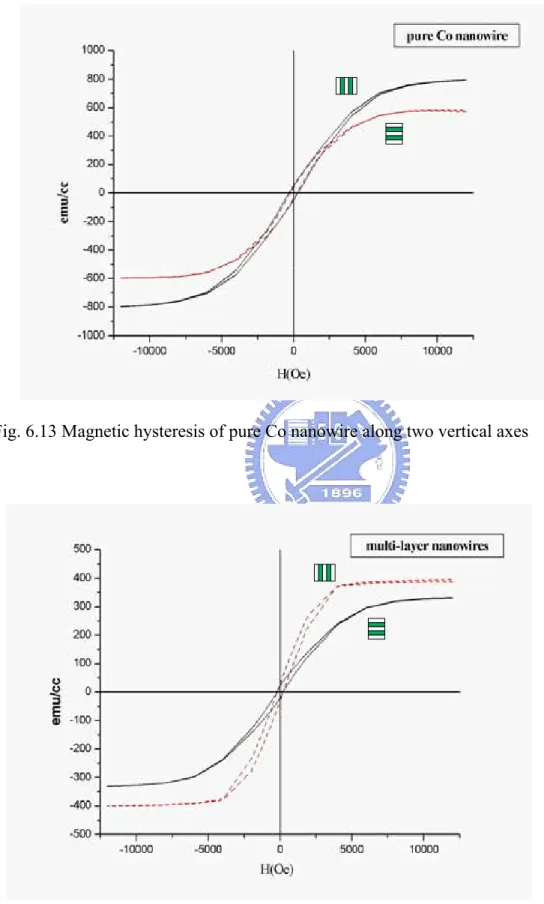
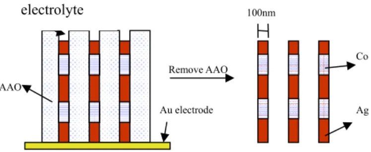
In chapter 6, a single bath electrodeposition method was developed to integrate nanowires of Ag/Co with multi-layer structures within a commercial AAO (anodic alumina oxide) template, with a pore diameter 100~200 nm. An electrolyte system containing silver nitride and cobalt sulfide was explored by using cyclic-voltammetry and electrodeposition rate to optimize electrodeposition conditions. A designed step-wise potential and different cations ratio [Co2+] / [Ag+] were adopted for the electrodeposition. After dissolution by NaOH, Ag/Co multilayered nanowires were obtained with a composition {[Co]/[Ag80Co20]}30 identified by XRD and TEM when
[Co2+] / [Ag+] = 150. By annealing at 200oC for 1hr, the uniformly structured {Co99.57/Ag100}30 nanowires were obtained. Compared with pure Co nanowire, the
magnetic hysteresis loops showed manifest magnetic anisotropy for {Co99.57/Ag100}30
nanowires than that of pure Co nanowires corresponding to a change of easy axis upon magnetization.
In chapter 7, The heterojunction photovoltaic devices consist of hybrid p-type organic Cu-phthalocyanine and inorganic n-type semiconductor ZnO nanostructures which include vertically aligned nanorods, randomly oriented nanorods and nanoparticles. The strong absorption of ZnO appears in 250~460nm wavelength and Cu-phthalocyanine exhibits broad absorption in 440-700nm with an absorption maximum at 630nm. The incorporation of partial Al into ZnO leads to the shift of
absorb light from UV region to visible light and subsequently causes more charge generation. Charge recombination from hybrid devices of vertically aligned ZnO nanorods was more efficient than that fabricated from the other types. The maximum incident photon to electron conversion and energy conversion efficiencies under simulated sunlight AM1.5 (10mW/cm2) in aligned ZnO are 0.036mA and 1.32%, respectively.
In chapter 8, a new 1 and 2 dimension nano structure for making solar cell or TFT module have been researched by adopting low cost coated glass substrate with polysilicon instead of silicon wafer. Meanwhile, laser annealing is used as the unique method to melt primal amorphous silicon thin film and promote it recrystalize under low temperature. Particularly, the new thermal conducting layers are patterned under the silicon layer to enhance the lateral giant grain growth. The important processes are represented as follows: 1. A electrical conducting layer are formed on the glass substrate. 2. Photolithographic process is executed to pattern the thermal conducting layer and form many variable thermal conducting zone. 3. An about 200nm amorphous silicon film is formed on the patterned thermal conductive layer. 4. A thermal isolation layer such as SiO2 is deposited for keeping laser annealing temperature. 5. While the pulse excimer laser is injected the structure, the amorphous silicon film can absorb laser energy instantaneously and transform it to crystalline type. Moreover, the temperature gradient could be generated on the silicon layer and cause the uniform polysilicon growth of 1~2µm giant grains under about 450-475mJ/cm2 laser fluence. A unique method of multiple laser fluence have been executed to increase the crystalline orientation of Si(111).
零維暨一維奈米材料之光電磁特性及結構研究 學生:林士欽 指導教授:陳三元教授 國立交通大學 材料科學及工程學系 摘要 奈米所具有之量子尺寸效應、表面界面效應等特殊現象,使奈米之光電材 料展現微米顆粒所不及之光電及催化特性,因顆粒尺寸減少時,對於紫外光之吸 收產生藍移現象,使能隙擴大,並產生更大之氧化還原電位;此外,而粒徑減少 時表面積增大,促進光電轉換,且吸附待分解物之能力增強,使光催化分解之效 率亦隨之增加;另外,尺寸減少時,光激發而形成之電子電洞對擴散至表面的時 間愈短,電子與電洞分離之效果愈好,進而提升光電效率。在奈米磁性材料之研 究方面,高深寬比的奈米磁導線,因為可以磁操控的關係所以可以將高深寬比的 銀鈷導線拉直,就因為如此可將此種導線,有高的導電異向性,因此可應用在超 細間距異向性導電膜為高密度磁記憶體及覆晶構裝重要材料。本文用bottom-up 之方法製作零維奈米結構(如金屬和半導體奈米粒子及自聚核/殼奈米粒子)及一 維奈米結構(如奈米管、奈米線、奈米棒),擁有許多新穎之特性及做為電子、磁 性、光學及化學性質之應用。一方面研究其製程之穩定性及發展性,另一方面也 發展其奈米特性進一步發展組裝新穎功能奈米材料的能力。進一步考量各重要材 料介面(如金屬-半導體,有機-無機等)後衍伸出來各種豐富的功能性,將可 能使許多發展中的奈米科學及科技應用產生巨大的改變,主要應用於太陽電池、 光觸媒、遠紅外線放射及磁性元件等。
第二章以多組分之ZrO2, TiO2, ZnO and Al2O3為起始原料,利用雷射剝離法 製作複晶相遠紅外線奈米材料。包括雷射劑量與氣氛等製程參數將影響生成之微 粉大小、形態與組成。形成之複晶相奈米材料之粒徑分布成雙峰分布,約7~15 nm (70~80%) and 40~100 nm (20~30%)。於低雷射劑量時有Zn組成富集且粒徑分布 窄化之趨勢,而隨雷射劑量增加,Zr組成亦隨之增加。而靶材之結構演變、及劑 量為控制奈米材料演化之重要因子。
第三章以液相電位分散及金屬鹽類還原之方法合成 TiO2於奈米級貴重金屬 樹枝狀結構之微粒上,形成全時效型光觸媒。研究結果顯示以金屬鹽類還原法較 光照還原法形成貴金屬樹枝狀結構之微粒,再利用負電位控制奈米 TiO2於奈米 級貴屬樹枝狀結構之微粒上為佳。針對滅菌能力、空氣及液相污染物的降解能力 來評估全時效型光觸媒的去除效能,以結合分散良好之 10 奈米 TiO2左右之奈米 貴重金屬與光觸媒載體效能最佳,隨奈米金屬粒徑增加而降低其去除效能。而對 次甲基藍分解效率亦可分別達到 99%以上。 第 四章使用次微米至奈米 級 孔 洞的氧化鋁模板,以含 NiSO4, NaH2PO2, NaC2H3O2 and Na3C6H5O7之亞磷酸鹽電解質溶液,在 80–100°C 與 pH = 3–6 條件 下合成磷酸鎳奈米管陣列。奈米管具有 1µm 長度、200-300nm 直徑與 80-150nm 管壁厚度。穿透式電子顯微鏡顯示奈米管由約 5nm 的粒子所組成。經 95%N2 /5%H2 氣氛與 500°C 溫度處理,奈米管陣列有 200Oe 的矯頑磁場與垂直奈米管方向易 磁化的磁異方性。隨處理溫度升高至 900°C,矯頑場與飽和磁化呈下降趨勢。 第五、六章以奈米模板(Nano template)陽極處理氧化鋁為基礎,使用電 鍍生成奈米銀線陣列的方式,電鍍鈷奈米線後,因鈷金屬可帶有磁效應,利用的 此性質即可製做出可以磁操控。在導電性上,可保有部分銀線的導電奈米導線, 並且以 AAO 當過模板的作法,可製造出高深寬比的奈米導線,因為可以磁操控的 關係所以可以將高深寬比的銀鈷導線拉直,就因為如此可將此種導線,有高的導 電異向性,因此可應用在超細間距異向性導電膜,為高密度磁記憶體及覆晶構裝 重要材料。規則的銀、銀/鎳、銀/鈷陣列利用脈衝電化學沉積在多孔的氧化鋁模 板從一個水溶性 Ag(NO3)2 和 Ac(NH3) 電鍍液中製作,移出模板,銀、銀/鎳、銀
/鈷奈米線陣列在 1.6~2.6V 和 40~90℃之條件使用,將 CoSO4,NiSO4, NiCl2 和
H3BO3 電鍍液,以形成殼核或多層之結構。15nm 鎳薄膜匹覆在直徑 200nm 之銀奈
米線上,形成殼核結構,依據 TEM 之結果顯示它是被發現已被鎳金屬匹覆之銀奈 米線之的磁性性質與傳統的純銀線相互比較其磁性性質能被加強。從磁力顯微鏡 影像是被觀察到銀-鎳核殼奈米線之 domain 狀態。另外, 銀-鎳奈米線顯示
180Oe 之矯頑磁場,施加磁場平行與垂直至奈米線幾乎是獨立的。無論如何,鎳 層能產生一個較大磁 domain 是被發現,變成平行方向超越垂直方向。 第七章以 N 型氧化鋅奈米線陣列與 P 型有機光電轉換材料結合,形成混成 太陽電池元件,以鋁摻雜之方式,使氧化鋅奈米線陣列對光之吸收峰往可見光部 分偏移,增加其對可見光之吸收率,並使元見之光電轉換效率、光電流和填充因 子有所提昇。 第八章利用新的一維及二維奈米結構為做太陽能電池或 TFT 模組,通過採 取便宜的鍍膜的玻璃基板,研究了於其上成長之多晶矽取代矽基板。同時,利用 雷射退火,快速熔融最初玻璃基板的矽薄膜和促進它的獨特的方法在低溫之下再 結晶,特別使用熱傳導層使之促進巨晶多晶矽之生長。重要製程如下: 1. 電子 傳導層在玻璃基體形成。 2. 黃光微影過程被形成,造成許多熱導變化的熱傳導 區域。3. 200nm 非晶矽薄膜形成熱導層數之上。 4. 保溫層如 SiO2 為保留雷射 退火溫度於矽薄膜之上形成。 5. 當雷射脈衝(excimer laser)入射此結構時, 非晶矽薄膜可瞬間地吸收激光能和變換成結晶型。 而且,利用溫度差及非晶矽 對於 234nm 波段對於雷射波段之吸收作用,於 450-475mJ//cm2 雷射脈衝之下, 在非晶矽薄膜層能引起和大約導致 1~2μm 巨大之多晶矽成長,而利用另一種複 合雷射劑量的方法,將可以增加 Si (111)順向優選排列取向。
Acknowledgments
I deeply appreciate to my supervisor professor Dr. San-Yuan Chen for his all-out supports. He is not only a benevolent advisor but also a very erudite philosopher. I also sincerely thank Dr. Syh-Yuh Cheng of the Industry Technology Research Institution for his warmhearted help in my thesis work. Moreover, I am grateful to Prof. Dr. Hong-Wen Wang, Dr. Pang Lin and Dr. Tien-Mo Liu for giving me much suggestion to my thesis content. Therefore, I would like to thank my colleagues in MCL and school. Finally, I wand to thank my family and friends for their selfless supports and encouragement during my study period.
Contents
Abstract I Abstract(Chinese) V Acknowledgments IX Contents X 1 Introduction 11.1 Strategies for one dimensional nanostructure growth 3
1.2 Negative template methods 4
1.3 Applications of the nanowires 5
1.4 Reference 15
2 Characterization and Composition Evolution of Multiple-Phase Nanoscaled Ceramic Powder by Laser Ablation 21
2.1 Introduction 21
2.2 Experimental 22
2.3 Results and discussion 22
2.4. Summary 26
3 Nanoscaled TiO2/Ag catalyst and photodecomposition characteristic 34
3.1 Introduction 34
3.2 Experimental 34
3.3 Results and discussion 36
3.4. Summary 39
4 Synthesis and magnetic properties of highly arrayed nickel-phosphate nanotubes 48
4.2 Experimental 49
4.3 Results and discussion 49
4.4. Summary 52
5 Electrochemical fabrication and magnetic properties of highly ordered silver-nickel core-shell nanowires 60
3.1 Introduction 60
3.2 Experimental 61
5.3 Results and discussion 62
5.4. Summary 66
6 Synthesis of Ag/Co magnetic nanowires with multi-layered structure 73
6.1 Introduction 74
6.2 Experimental 75
6.3 Results and discussion 76
6.4. Summary 78
7 Solar cell devices based on Cu-phthalocyanine / nanostructured ZnO hybrid film 91
7.1 Introduction 91
7.2 Experimental 92
7.3 Results and discussion 93
7.4. Summary 96
8.1and 2 Dimention Nano Structure Design and Giant-Grain Orientated Polysilicon Study at Low Temperature……… 102
8.1 Introduction 102
8.2 Experimental 103
8.3 Results and discussion 103
9 Conclusion 115 10.Publication list 118
Chapter 1
Introduction
Particles with nanometer-scale size have large ratio of surface to bulk atoms. Large surface always gives high active behavior and changes both physical and chemical properties. Inorganic nanoparticles having size generally smaller than 100nm provide superior properties for various applications and become important topic in nanomaterials.
Many methods are developed to prepare inorganic nanoparticles during recent year. Chemical route includes metal-organic compounds the so-called precursors and reaction through hydrolysis, condensation, catalysis, pyrolysis, etc . Evaporation-condensation is mainly the process in physical route and laser ablation is the important method included in this route.[2-5] The far-infrared ray emissivity and photodecomposition characterization of nanoparticles based on oxide system was deeply investigated recently.
Moreover, magnetic film and nanowires have been the most interesting and intensely investigated fields of material in recent year . The fabrication of magnetic metal arrays has not only the fundamental worth in these materials but also their potential utilization in magnetic recording. For high density storage media, one single nanosized pattern, ordered nanodots or nanotubes is a single domain structure and denotes one bit signal. Magnetic period nano-structure arrays as an ultra-high-density magnetic storage can achieve recording densities of more than 100Gbit/in2, which is more than the continuous magnetic film of 40Gbit/in2. Arrays of ferromagnetic nonodots, nanowires or nanotubes may be fabricated by several methods such as e-beam lithography, imprint technology or template. The porous template can be considered as one quicker and cheaper method to prepare highly perpendicular magnetic anisotropy structure because AAO(anode alumina oxide) has high oriented porous structure with uniform and nearly parallel pores that can be organized the pseudo ordered nanowire or nanotube arrays. Such
structure also shows high magnetic anisotropy phenomena with the shape axis parallel to the nanowire arrays.
On the other hand, it is well known that transition metals such as Fe, Co, Ni and their alloy have higher saturation magnetization as well as Curie temperature, and lower crystalline anisotropy. Furthermore, magnetic properties are strongly influenced by the dimension and crystal properties, which also depend on the physical structure of templates and growth mechanism of wires or tubes. Recently, magnetic properties of nickel nanowires have been investigated by several groups because nickel nanowires show important applications in magnetic recording.
Organic-inorganic hybrids for photovoltaic cell have been receiving attention recently. It has become the major purposes to enhance the conversion efficiency of the photovoltaic devices and at same time to reduce production costs. Semiconductor oxide materials in conjunction with photo sensitive organic dyes have extended hybrid materials sensitivity into the visible regions. ZnO is a semiconductor material and possesses special characteristic including high electron mobility, low temperature synthesis, and the potential for controlling the morphology through simple solution processing. In the past few years, hybrid devices including ZnO/ZnPc, ZnO/merocyanines, ZnO/P3HT and ZnO/CuPcetc, have been constantly investigated. The obtained hybrid ZnO/ dye devices have an overall efficiency of approximately 0.2-2% and fill factor of greater than 0.3-0.6 and 5~16% of the external quantum efficiency that could be attributed to the increased ZnO /dye interfacial area due to recombination behaviors of high surface ZnO structure. However, the conversion efficiency of these devices have been limited because of difficultly controllable particle boundary, inorganic/dye degradation and high production costs. In recent years, ZnO nanorods or nanowires uniformly grown perpendicular to the substrate are particularly investigated because of slow charge recombination between aligned nanowires and dyes that results in significant improvements in device performance.
1.1 Strategies for one dimensional nanostructure growth
One dimensional nanostructure with different levels of control over these parameters. Figure 1 schematically illustrates some of these synthetic strategies that include:(1) use of the intrinsically anisotropic crystallographic structure of a solid to accomplish one dimensional growth(Fig. 1.1.A); (2) introduction of a liquid-solid interface to reduce the symmetry of a seed(Fig. 1.1.B); (3) used of various templates with one dimensional morphologies to direct the information of one dimensional nanostructure (Fig. 1.1.C); (4) use of supersaturation control to modify the growth habit of a seed; (5) use of appropriate capping reagent to kinetically control the growth rates of various facets of a seed(Fig. 1.1.D); (6)self-assembly of zero dimensional nanostuctures(Fig. 1.1.E); (7) size reduction of one dimensional microstructure(Fig. 1.1.F). Because many of these methods were not demonstrated until very recently, most of their characteristics are only vaguely known.
One-dimensional nanomaterials based on template synthesis have attracted much research interest. Porous alumina membranes are widely used as templates for fabricating one-dimensional nanostructures, including metals, semiconductors, carbon, and conductive polymers. However, the alumina membrane itself has several disadvantages, such as insufficient chemical stability and low mechanical strength. It is therefore difficult to use alumina membranes for the synthesis of nanowires and nanotubes under severe reaction conditions such as in strong acid and alkali solutions. To overcome these disadvantages, a two-step replication process was developed. Although this has resulted in the successful fabrication of nanoporous replicated films, there are still some disadvantages. Usually, it is very hard to achieve full replication of the alumina membrane, thus resulting in poor aspect ratio (typically less than 100) of the replicated films. Moreover, the methyl methacrylate MMA) monomer, which is used as the replication medium, is injected into the pores under vacuum conditions. Thus the replication process is complicated and this makes it difficult to be applied widely in industrial
manufacturing processes in Fig. 1.2. A widely used approach to fabricate metal nanowires is based on various templates, which include negative, positive, and surface step templates. We discuss each of the approaches below.
1.2 Negative template methods
Negative template methods use prefabricated cylindrical nanopores in a solid material as templates. By depositing metals into the nanopores, nanowires with a diameter predetermined by the diameter of the nanopores are fabricated. There are several ways to fill the nanopores with metals or other materials to form nanowires, but the electrochemical method is a general and versatile method. If one dissolves away the host solid material, free-standing nanowires are obtained. This method may be regarded as a “brute-force”method because the diameter of the nanowires is determined by the geometrical constraint of the pores rather than by elegant chemical principles. However, it is one of the most successful methods to fabricate various nanowires that are difficult to form by conventional lithographic process. Fabrication of suitable templates is clearly a critical first step. To date, a number of methods have been developed to fabricate various negative templates. Examples include alumina membranes, polycarbonate membranes, mica sheets, and diblock polymer materials. These materials contain a large number of straight cylindrical nanopores with a narrow distribution in the diameters of the nanopores.
Anodic porous alumina is commonly used negative template. The nanopores in the template are formed by anodizing aluminum films in an acidic electrolyte. The individual nanopores in the alumina can be ordered into a close-packed honeycomb structure (Fig. 1.3). The diameter of each pore and the separation between two adjacent pores can be controlled by changing the anodization conditions. The fabrication method of anodic porous alumina can be traced back to the work done in the 1950’s, which involves a one-step anodization process. This original one-step anodization method is still used to fabricate most commercial alumina membranes [1.1, 1.2]. The anodic porous alumina has a much higher pore density ( 1011 pores/cm2), which allows one to fabricate a large number of nanowires at one time. Another interesting feature of the
porous alumina template is that the chemistry of the pore walls can be altered via reaction with silane compounds [1.3]. The distribution of nanopores in anodic porous alumina is usually not as perfect as the one shown in Figure 1.3. To achieve highly ordered pores, high-purity aluminum films (99.999%) are used. In addition, they are first preannealed to remove mechanical stress and enhance the grain size. Subsequently, the films are electropolished in a 4:4:2 (by weight) mixture of H3PO4, H2SO4, and H2O to create homogeneous surfaces. Without the preannealing and
electropolishing steps, it is hard to form well-ordered pores [1.4]. The order of the pores depends also on other anodization conditions, such as anodization voltage and electrolyte. It has been reported that anodization over a long period at an appropriate constant voltage can produce an almost ideal honeycomb structure over an area of several µm [1.4, 1.5]. The optimal voltage depends on the electrolyte used for the anodization. For example, the optimal voltage for long-range ordering is 25 V in sulfuric acid, 40 V in oxalic acid, and 195 V in phosphoric acid electrolyte, respectively [1.4]. The diameter and depth of each pore, as well as the spacing between adjacent pores can be also controlled by the anodizing conditions. Both the pore diameter and the pore spacing are proportional to the anodizing voltage with proportional constants of 1.29 nm V−1 and 2.5 nm V−1, respectively. The dependence of the diameter and the spacing on the voltage is not sensitive to the electrolyte, which is quite different from the optimal voltage for ordered distribution of the pores as discussed above [1.6,1.7]. This property has been exploited to make size-selective microfiltration membranes and to control the diameter of nanowires formed in the pores. By properly controlling the anodization voltage and choosing the electrolyte, one can make highly ordered nanopores in alumina with desired pore diameter and spacing. The order of the pores achieved by anodizing an aluminum film over a long period is often limited to a domain of several _m. The individual ordered domains are separated by regions of defects. Recently, a novel approach has been reported to produce a nearly ideal hexagonal nanopore array that can extend over several millimeters [1.8, 1.9]. The approach uses a pretexturing process of Al in which an array of shallow concave features is initially formed on
Al by indentation. These concave features serve as nucleation sites for the formation of pores during the initial stage of anodization. The pore spacing can be controlled by the pretextured pattern and the applied voltage. Another widely used method to create highly ordered nanopore arrays is a two-step anodization method [1.10,1.11]. The first step involves a long-period anodization of high purity aluminum to form a porous alumina layer. Subsequent dissolution of the porous alumina layer leads to a patterned aluminum substrate with an ordered array of concaves formed during the first anodization process. The ordered concaves serve as the initial sites to form a highly ordered nanopore array in a second anodization step. Acidic anodization of Al normally results in a porous alumina structure which is separated from the aluminum substrate with a so-called barrier layer of Al2O3. The barrier layer and aluminum substrate can be
removed to form a free-standing porous alumina membrane. The aluminum can be removed with saturated HgCl2 and the barrier layer of Al2O3 with a saturated solution of KOH in ethylene
glycol. An alternative strategy to separate the porous alumina from the substrate is to take advantage of the dependence of pore diameter on anodization voltage. By repeatedly decreasing the anodization voltage several times at 5% increments, the barrier layer becomes a tree-root-like network with fine pores. Since the root-like network has a higher exposed surface area than the primary large pores, dissolution occurs there first when immersing the sample in a concentrated acid. The dissolution of the network then results in the separation of the porous oxide film from the aluminum substrate.
Fabrication of Metal Nanowires Using the membrane templates previously described, nanowires of various metals, semiconductors and conducting polymers [1.12], have been fabricated. These nanostructures can be deposited into the pores by either electrochemical deposition or other methods, such as chemical vapor deposition (CVD) [1.13], chemical polymerization, electroless deposition [1.14], or by sol–gel chemistry. Electrodeposition is one of the most widely used methods to fill conducting materials into the nanopores to form continuous nanowires with large aspect ratios. One of the great advantages of the
electrodeposition method is the ability to create highly conductive nanowires. This is because electrodeposition relies on electron transfer, which is the fastest along the highest conductive path. Structural analysis showed that the electrodeposited nanowires tend to be dense, continuous, and highly crystalline in contrast to other deposition methods, such as CVD. Yi and Schwarzacher demonstrated that the crystallinity of superconducting Pb nanowires can be controlled by applying a potential pulse with appropriate parameters [1.15]. The electrodeposition method is not limited to nanowires of pure elements. It can fabricate nanowires of metal alloys with good control over stoichiometry. For example, by adjusting the current density and solution composition, Huang et al. controlled the compositions of CoPt and FePt nanowires to 50:50 in order to obtain the high anisotropic face-centered tetragonal phases [1.16]. Similar strategies have been used in other magnetic nanowires [1.17,1.18] and in thermoelectronic nanowires [1.19]. Anotherimportant advantage of the electrodeposition method is the ability to control the aspect ratio of the metal nanowires by monitoring the total amount of passed charge. This is important for many applications. For example, the optical properties of nanowires are critically dependant on the aspect ratio [1.20]. Nanowires with multiple segments of different metals in a controlled sequence can also be fabricated by controlling the potential in a solution containing different metal ions [1.21]. Electrodeposition often requires one to deposit a metal film on one side of the freestanding membrane to serve as a working electrode on which electrodeposition takes place. In the case of large pore sizes, the metal film has to be rather thick to completely seal the pores on one side. The opposite side of the membrane is exposed to an electrodeposition solution, which fills up the pores and allows metal ions to reach the metal film. However, one can avoid using the metal film on the backside by using anodic alumina templates with the natural supporting Al substrate. The use of the supported templates also prevents one from breaking the fragile membrane during handling. However, it requires one to use AC electrodeposition [1.22]. This is because of the rather thick barrier layer between the nanopore membrane and the Al substrate. Detailed studies of the electrochemical fabrication process
nanowires have been carried out by a number of groups [1.23]. The time dependence of the current curves recorded during the electrodeposition process reveal three typical stages. Stage I corresponds to the electrodeposition of metal into the pores until they are filled up to the top surface of the membrane. In this stage, the steady-state current at a fixed potential is directly proportional to the metal film area that is in contact with the solution, as found in the electrodeposition on bulk electrodes. However, the electrodeposition is confined within the narrow pores, which has a profound effect on the diffusion process of the metal ions from the bulk solution into the pores before reaching the metal film. The concentration profiles of Co ions in the nanopores of polycarbonate membranes during electrodeposition of Co have been studied by Valizadeh et al. [1.24]. After the pores are filled up with deposited metal, metal grows out of the pores and forms hemispherical caps on the membrane surface. This region is called stage II. Since the effective electrode area increases rapidly during this stage, the electrochemical current increases rapidly. When the hemispherical caps coalescence into a continuous film, stage III starts, which is characterized by a constant value again. By stopping the electrodeposition process before stage I ends, an array of nanowires filled in the pores is formed. The current-time curves are not always as well behaved as the one described above [1.25]. For example, the current may vary during the first stage, so that stages I, II, and III may merge together and become difficult to separate. One plausible explanation of this observation is that the pores in the membranes are not aligned parallel but have a considerable angular distribution (±34_). The angular distribution means a large length distribution of the pores, such that the pores with different lengths fill up with nanowires at different times. Another possible reason is inhomogeneous growth rates in different pores, due to different degrees of wetting of different pores. The wetting problem tends to be more severe for membranes with smaller pores because of the increased difficulty to wet all the pores before electrodeposition. One way to reduce the wetting problem is to treat polycarbonate membranes with polyvinylpyrrolidone (PVP) [1.25]. Adding ethanol or methanol into the electrolyte is also found to reduce the wetting problem
[1.26]. Another method is to perform the electrodeposition in an ultrasound bath to facilitate the mass transport of ions through the pores of the membrane [1.27].
1.3 Applications of the nanowires
Metal nanowires are promising materials for many novel applications, ranging from chemical and biological sensors to optical and electronic devices. This is not only because of their unique geometry, but also because they possess many unique physical properties, including electrical, magnetic, optical, as well as mechanical properties. While most efforts to date have focused on developing better methods to fabricate the nanowires and on characterizing the various properties, applications are becoming an important area of research and development. Some of the applications are discussed below.
1.3.1. Magnetic Materials and Devices
The electrodeposition methods described above have been used to fabricate magnetic nanowires of a single metal [1.28], multiple metals in segments [1.29], as well as alloys [1.30]. Since the pioneering works nearly a decade ago, much progress has been made in understanding the magnetic properties of the nanowires [1.31]. Arecent review provides a detailed description of the properties [163]. For magnetic nanowires (Fe, Co, and Ni) with relative large aspect ratios (e.g., >50), they exhibit an easy axis along the wires. An important parameter that describes magnetic properties of materials is the remanence ratio, which measures the remanence magnetization after switching off the external magnetic field. The remanence ratios of the Fe, Co, and Ni nanowires can be larger than 0.9 along the wires and much smaller in the perpendicular direction of the wires. This finding clearly shows that the shape anisotropy plays an important role in the magnetism of the nanowires. Another important parameter that describes the magnetic properties is coercivity, which is the coercive field required to demagnetize the magnet after full magnetization. The magnetic nanowires exhibit greatly enhanced magnetic coercivity [1.32, 1.33]. In addition, the coercivity depends on the wire diameter and the aspect ratio, which shows that it is possible to control the magnetic properties of the nanowires by controlling the
fabrication parameters. The diameter dependence of the coercivity reflects a change of the magnetization reversal mechanism from localized quasi-coherent nucleation for small diameters to a localized curling like nucleation as the diameter exceeds a critical value [1.34]. Another technically important novel property observed in the magnetic nanowires is giant magnetoresistance (GMR) [1.29]. For example, Evans et al. have studied Co-Ni-Cu/Cu multilayered nanowires and found a magnetoresistance ratio of 55% at room temperature and 115% at 77K for current perpendicular to the plane (along the direction of the wires) [1.35]. Giant magnetoresistance has also been observed in semimetallic Bi nanowires fabricated by electrodeposition [1.36]. Hong et al. have studied GMR of Bi with diameters between 200 nm and 2µm in magnetic fields up to 55T and found that the magnetoresistance ratio is between 600–800% for magnetic field perpendicular to the wires and 200% for the field parallel to the wires [1.37]. The novel properties and small dimensions have potential applications in the miniaturization of magnetic sensors and the high-density magnetic storage devices. The alignment of magnetic nanowires in an applied magnetic field can be used to assemble the individual nanowires [1.38]. Tanase et al. studied the response of Ni nanowires in response to magnetic field [1.39]. The nanowires are fabricated by electrodeposition using alumina templates and functionalized with luminescent porphyrins so that they can be visualized with a video microscope. In viscous solvents, magnetic fields can be used to orient the nanowires. In mobile solvents, the nanowires form chains in a head-to-tail configuration when a small magnetic field is applied. In addition, they demonstrated that three-segment Pt-Ni-Pt nanowires can be trapped between lithographically patterned magnetic microelectrodes [1.40]. The technique has a potential application in the fabrication and measurement of nanoscale magnetic devices.
1.3.2. Optical Applications
Dickson and Lyon studied surface plasmon (collective excitation of conduction electrons) propagation along 20 nmdiameter Au, Ag, and bimetallic Au-Ag nanowires with a sharp Au/Ag heterojunction over a distance of tens of µm [1.41]. The plasmons are excited by focusing a laser
with a high numerical aperture microscope objective, which propagate along a nanowire and reemerge as light at the other end of the nanowire via plasmon scattering. The propagation depends strongly on the wavelength of the incident laser light and the composition of the nanowire. At the wavelength of 820 nm, the plasmon can propagate in both Au and Ag nanowires, although the efficiency in Ag is much higher than that in Au. In the case of bimetallic nanowire, light emission is clearly observed from the Ag end of the nanowire when the Au end is illuminated at 820 nm. In sharp contrast, if the same bimetallic rod is excited at 820 nm via the Ag end, no light is emitted from the distal Au end. The observation suggests that the plasmon mode excited at 820 nm is able to couple from the Au portion into the Ag portion with high efficiency, but not from the Ag portion into Au. The unidirectional propagation has been explained using a simple two-level potential model. Since surface plasmons propagate much more efficiently in Ag than in Au, the Au→ Ag boundary is largely transmissive, thus enabling efficient plasmon propagation in this direction. In the opposite direction, however, propagation from Ag to Au gains a much steeper potential wall, allowing less optical energy to couple through to the distal end. Their experiments suggest that one can initiate and control the flow of optically encoded information with nanometer-scale accuracy over distances of many microns, which may find applications in future high-density optical computing.
1.3.3. Biological Assays
We have mentioned that by sequentially depositing different metals into the nanopores, multisegment or striped metal nanowires can be fabricated [1.27]. The length of each segment can be controlled by the charge passed in each plating step and the sequence of the multiple segments is determined by the sequence of the plating steps. Due to the different chemical reactivities of the “stripe” metals, these stripes can be modified with appropriate molecules. For example, Au binds strongly to thiols and Pt has high affinity to isocyanides. Interactions between complementary molecules on specific strips of the nanowires allow different nanowires to bind to each other and form patterns on planar surfaces. Using this strategy, nanowires could assemble
deterministically into cross- or T-shaped pairs, or into more complex shapes [1.41]. It is also possible to use specific interactions between selectively functionalized segments of these nanowires to direct the assembly of nanowire dimers and oligomers, to prepare two-dimensional assembly of nanowire-substrate epitaxy, and to prepare threedimensional colloidal crystals from nanowire-shaped objects [1.42]. As an example, single-stranded DNA can be exclusively modified at the tip or any desired location of a nanowire, with the rest of the wire covered by an organic passivation monolayer. This opens the possibility for site specific DNA assembly [1.27]. Nicewarner-Pena et al. showed that the controlled sequence of multisegment nanowires can be used as “barcodes” in biological assays [1.43]. The typical dimension of the nanowire is 200 nm thick and 10 µm long. Because the wavelength dependence of reflectance is different for different metals, the individual segments are easily observed as “stripes” under an optical microscope with unpolarized white-light illumination. Different metal stripes within a single nanowire selectively adsorb different molecules, such as DNA oligomers, which can be used to detect different biological molecules simultaneously. These multisegment nanowires have been used like metallic barcodes in DNAand protein bioassays. The optical scattering efficiency of the multisegment nanowires can be significantly enhanced by reducing the dimensions of the segment, such that the excitation of the surface plasmon occurs. Mock et al. [1.44] have studied the optical scattering of multisegment nanowires of Ag, Au, and Ni that have diameters of 30 nm and length up to 7µm. The optical scattering is dominated by the polarization-dependant plasmon resonance of Ag and Au segments. This is different from the case of the thicker nanowires used by Nicewarner-Pena et al., where the reflectance properties of bulk metals determine the contrast of the optical images [1.43]. Because of the large enhancement by the surface plasmon resonance, very narrow ( 30 nm diameter) nanowires can be readily observed under white light illumination and the optical spectra of the individual segments are easily distinguishable [1.44]. The multisegment nanowires can host a large number of segment sequences over a rather small spatial range, which promises unique applications.
1.3.4. Nanoelectronic and Nanoelectrochemical Applications
In addition to multisegment metal nanowires, one can also fabricate a metal/organic film/metal junction [1.45] and metal/nanoparticle/metal junctions [1.46] in a single nanowire, which have been used to study electron transport properties of the small amount of molecules and nanoparticles. It has been demonstrated that a Au nanowire containing 4-_[2-nitro-4 (phenylethynyl) phenyl ethynyl_benzenethiol molecule junction exhibits negative differential resistance at room temperature [1.47], while a 16-mercaptohexadecanoic acid nanojunction exhibits a coherent nonresonant tunneling [1.48]. If some of the metal segments or “stripes” are being replaced with semiconductor, colloidal, and polymer layers, one can introduce rectifying junctions, electronic switching, and photoconductive elements in the composite nanowires. If selectively modifying the nanowire further, using the distinct surface chemistry of different stripes, the nanowires can be positioned on a patterned surface to fulfill nano-logic and memory circuits by self-assembling [1.46, 1.49]. An array of metal nanowires can be used as a nanoelectrode array for many electrochemical applications [1.50]. For this purpose, a large array of nanowires with long-range hexagonal order fabricated with the anodic alumina templates is particularly attractive.
1.3.5. Chemical Sensors
Penner, Handley, and Dagani et al. exploited hydrogen sensor applications using arrays of Pd nanowires [1.50,1.52]. Unlike the traditional Pd-based hydrogen sensor that detects a drop in the conductivity of Pd upon exposure to hydrogen, the Pd-nanowire sensor measures an increase in the conductivity. The reason is because the Pd wire consists of a string of Pd particles separated with nanometer-scale gaps. These gaps close to form a conductive path in the presence of hydrogen molecules as Pd particles expand in volume. The volume expansion is well known, which is due to the disassociation of hydrogen molecules into hydrogen atoms that penetrate into the Pd lattice and expand the lattice. Although macroscopic Pd-based hydrogen sensors are
readily available, they have the following two major drawbacks. First, their response time is between 0.5 s to several minutes, which is too slow to monitor gas flow in real time. Second, they are prone to the poisoning of a number of gas molecules, such as methane, oxygen, and carbon monoxide, which adsorb onto the sensor surfaces and block the adsorption sites for hydrogen molecules. The Pd nanowires offer remedies to the above problems. They have a large surface-to-volume ratio, so the response time can be as fast as 20 ms. The large surface-to-volume ratio also make the nanowire sensor less prone to the poisoning by common contaminations.
1.4 Reference
[1.1] F. Keller, M. S. Hunter, and D. L. Robinson, J. Electrochem. Soc. 100, 411 (1953). [1.2] J. P. O’Sullivan and G. C. Wood, Proc. R. Soc. London, Ser. A 317, 511 (1970). [1.3] C. R. Martin, Acc. Chem. Res. 28, 61 (1995).
[1.4] O. Jessensky, F. Muller, and U. Gosele, Appl. Phys. Lett. 72, 1173 (1998). [1.5] H. Masuda and K. Fukuda, Science 268, 1466 (1995).
[1.6] A. R. Despic, J. Electroanal. Chem. Interfacial Electrochem. 191, 417 (1985). [1.7] R. C. Furneaux, W. R. Rigby, and A. P. Davidson, Nature 337, 147 (1989).
[1.8] D. Crouse, Y.-H. Lo, A. E. Miller, and M. Crouse, Appl. Phys. Lett. 76, 49 (2000).
[1.9] H. Masuda, H. Yamada, M. Satoh, H. Asoh, M. Nakao, and T. Tamamura, Appl. Phys. Lett. 71, 2770 (1997).
[1.10] H. Masuda and M. Satoh, Jpn. J. Appl. Phys. 35, L126 (1996).
[1.11. A.-P. Li, F. Muller, A. Birner, K. Nielsch, and U. Gosele, Adv. Mater. 11, 483 (1999). [1.12] L. S. Van Dyke and C. R. Martin, Langmuir 6, 1123 (1990).
[1.13] G. Che, B. B. Lakshmi, C. R. Martin, E. R. Fisher, and R. R.S., Chem. Mater. 10, 260 (1998).
[1.14] M. Wirtz, M. Parker, Y. Kobayashi, and C. R. Martin, Chem. Eur. J. 8, 353 (2002). [1.15. G. Yi and W. Schwarzacher, Appl. Phys. Lett. 74, 1746 (1999).
[1.16] Y. H. Huang, H. Okumura, and G. C. Hadjipanayis, J. Appl. Phys. 91, 6869 (2002).
[1.17] C. Z. Wang, G. W. Meng, Q. Q. Fang, X. S. Peng, Y. W. Wang, Q. Fang, and L. D. Zhang, J. Phys. D 35, 738 (2002).
[1.18] D. H. Qin, C. W. Wang, Q. Y. Sun, and H. L. Li, Appl. Phys. A-Mater. 74, 761 (2002). [1.19] M. S. Sander, A. L. Prieto, R. Gronsky, T. Sands, and A. M. Stacy, Adv. Mater. 14, 665
(2002).
[1.20] C. K. Preston and M. J. Moskovits, J. Phys. Chem. 97, 8495 (1993).
[1.22] K. H. Lee, H. Y. Lee, W. Y. Jeung, and W. Y. Lee, J. Appl. Phys. 91, 8513 (2002).
[1.23] P. Forrer, F. Schlottig, H. Siegenthaler, and M. Textor, J. Appl. Electrochem. 30, 533 (2000).
[1.24] S. Valizadeh, J. M. George, P. Leisner, and L. Hultman, Electrochim. Acta 47, 865 (2001). [1.25] C. Schonenberger, B. M. I. van der Zande, L. G. J. Fokkink, M. Henny, C. Schmid, M.
Kruger, A. Bachtold, R. Huber, H. Birk, and U. Staufer, J. Phys. Chem. B 101, 5497 (1997). [1.26] T. Thurn-Albrecht, J. Schotter, G. A. Kastle, N. Emley, T. Shibauchi, L. Krusin-Elbaum, K.
Guarini, C. T. Black, M. T.Tuominen, and T. P. Russell, Science 290, 2126 (2000).
[1.27] B. R. Martin, D. J. Dermody, B. D. Reiss, M. M. Fang, L. A. Lyon, M. J. Natan, and T. E. Mallouk, Adv. Mater. 11, 1021 (1999).
[1.28] T. M. Whitney, J. S. Jiang, P. C. Searson, and C. L. Chien, Science 261, 1316 (1993).
[1.29] L. Piraux, J. M. George, J. F. Despres, C. Leroy, E. Ferain, R. Legras, K. Ounadjela, and A. Fert, Appl. Phys. Lett. 65, 2484– 2486 (1994).
[1.30] S. Dubois, J. M. Beuken, L. Piraux, J. L. Duvail, A. Fert, J. M. George, and J. L. Maurice, J. Magn. Magn. Mater. 165, 30 (1997).
[1.31] S. Pignard, G. Goglio, A. Radulescu, and L. Piraux, J. Appl. Phys. 87, 824 (2000). [1.32] C. L. Chien, J. Appl. Phys. 69, 5267 (1991).
[1.33] T. Thurn-Albrecht, J. Schotter, C. A. Kastle, N. Emley, T. Shibauchi, L. Krusin-Elbaum, K. Guarini, C. T. Black, M. T. Tuominen, and T. P. Russell, Science 290, 2126 (2000).
[1.34] H. Zeng, R. Skomki, L. Menon, Y. Liu, S. Bandyopadhyay, and D. J. Sellmyer, Phys. Rev. B 65, 13426 (2002).
[1.35] P. R. Evans, G. Yi, and W. Schwarzacher, Appl. Phys. Lett. 76, 481 (2000).
[1.36] K. Liu, C. L. Chien, P. C. Searson, and Y. Z. Kui, Appl. Phys. Lett. 73, 1436 (1998). [1.37] K. Hong, F. Y. Yang, K. Liu, D. H. Reich, P. C. Searson, C. L. Chien, F. F. Balakirev, and
[1.38] Y. M. Lin, S. B. Cronin, J. Y. Ying, M. S. Dresselhaus, and J. P. Heremans, Appl. Phys. Lett. 76, 3944 (2000).
[1.39] M. Tanase, L. A. Bauer, A. Hultgren, D. M. Silevitch, L. Sun, D. H. Reich, P. C. Searson, and G. J. Meyer, Nano Lett. 1, 155 (2001).
[1.40] M. Tanase, D. M. Silevitch, A. Hultgren, L. A. Bauer, P. C. Searson, G. J. Meyer, and D. H. Reich, J. Appl. Phys. 91, 8549 (2002).
[1.41] B. D. Reiss, J. N. K. Mbindyo, B. R. Martin, S. R. Nicewarner,T. E. Mallouk, M. J. Natan, and C. D. Keating, Mate. Res. Soc.Symp. Proc., in press (2001).
[1.42]. J. S. Yu, J. Y. Kim, S. Lee, J. K. N. Mbindyo, B. R. Martin, and T. E. Mallouk, Chem. Commun. 2445 (2000).
[1.43] S. R. Nicewarner-Pena, R. G. Freeman, B. D. Reiss, L. He, D. J. Pena, I. D. Walton, R. Cromer, C. D. Keating, and M. J. Natan, Science 294, 137 (2001).
[1.44] J. J. Mock, S. J. Oldenburg, D. R. Smith, D. A. Schultz, and S. Schultz, Nano Lett. 2, 465 (2002).
[1.45] J. K. N. Mbindyo, T. E. Mallouk, J. B. Mattzela, I. Kratochvilova, B. Razavi, T. N. Jackson, and T. S. Mayer, J. Am. Chem. Soc. 124, 4020 (2002).
[1.46] N. I. Kovtyukhova, B. R. Martin, J. K. N. Mbindyo, T. E. Mallouk, M. Cabassi, and T. S. Mayer, Mater. Sci. & Eng. C 19, 255 (2002).
[1.47]. I. Kratochvilova, M. Kocirik, A. Zambova, J. Mbindyo, T. E. Mallouk, and T. S. Mayer, J. Mater. Chem. 12, 2927 (2002).
1.48] I. Kratochvilova, A. Zambova, J. Mbindyo, B. Razavi, and J. Holakovsky, Modern Phys. Lett. B 16, 161 (2002).
[1.49] N. I. Kovtyukhova and T. E. Mallouk, Chem. Euro. J. 8, 4355 (2002).
[1.50] K. Uosaki, K. Okazaki, H. Kita, and H. Takahashi, Anal. Chem. 62, 652 (1990).
[1.51] F. Favier, E. C. Walter, M. P. Zach, T. Benter, and R. M. Penner, Science 293, 2227 (2001).
[1.52] E. C. Walter, F. Favier, and R. M. Penner, Anal. Chem. 74, 1546 (2002).
Figure 1.1 schematically illustrates some of six synthetic strategies.
.
Fig.1.2 Schematic outline of the fabrication of nanoporous Ni film: (a) through-hole alumina membrane, (b) deposition of the Pd catalyst layer, (c) immersion of alumina membrane in MMA and pre-polymerization of MMA, (d) polymerization of MMA, (e) removal of alumina membrane and electroless metal deposition, (f) double-faced and single-faced nanoporous Ni films and (g) removal of PMMA.
Chapter 2
Characterization and Composition Evolution of Multiple-Phase Nanoscaled
Ceramic Powder by Laser Ablation
2.1 Introduction
Particles with nanometer-scale size have large ratio of surface to bulk atoms. Large surface always gives high active behavior and changes both physical and chemical properties. Inorganic nanoparticles having size generally smaller than 100nm provide superior properties for various applications and become important topic in nanomaterials.
Many methods are developed to prepare inorganic nanoparticles during recent year[2.1]. Chemical route includes metal-organic compounds the so-called precursors and reaction through hydrolysis, condensation, catalysis, pyrolysis, etc[2.2,2.3]. Evaporation-condensation is mainly the process in physical route [2.4] and laser ablation is the important method included in this route.[2.5] Nanoparticle of inorganic materials can easily be produced by laser ablation because inorganic materials can easily be evaporated by high energy laser beam and be subsequently condensed into particles. For complex or multiphase material, composition and phase of ablated particle are easily adjustable through composition/phase modification of target [2-6]. However, there will be phase separation occurred when multiphase or complex oxide is used as target. Therefore, modification of target composition is important to recover the composition of nanoparticle and upgrade the properties.
Ceramic particles of complex or multiphase oxide often possess multifunction that have been applied for far-infrared emission ceramic, fiber and many kind of textile. Material owned high efficiency far-infrared emission using transitional element oxide had been reported[2.7,2.8]. In this work, multiphase target composed of Al2O3, ZnO, TiO2 and ZrO2 is selected for the study. Target
microstructure and processing conditions including laser energy, chamber pressure, and flow rate of carrier gas will be investigated to composition, particle size distribution and phase of ablated
nanoparticles. In addition, The far-infrared emissivity characteristic of nanoparticles based on ZrTiO4--ZnAl2O4 system was investigated as functions of nanoparticle size, composition and
formation phase.
2.2 Experimental
Targets for the physical process of nanoparticle synthesis are made from conventional ceramic process. Oxides chosen from ZrO2, TiO2, ZnO and Al2O3 (all purity>99.5%) micropowders were
used as raw materials. The mixtures with the ratio of ZrO2:TiO2:ZnO:Al2O3= 1:1: 2: 2(ZAT1,mole
ratio) and 2: 2:1:1(ZAT2) were mixed and then compressed into 30mm diameter green compaction. After calcination at 1100oC, disk-type sample was press-formed and then sintered at 1300oC for 2h to make dense target for laser ablation.
Excimer laser (248nm) power is varied to study the ablation efficiency for different materials. The laser irradiation conditions of 0~4 J/cm2 were used in this work. Three gases, air, oxygen and nitrogen, were used for carrier gas (set up flow rate 2L/min) with remained ambient atmospheres around 1 atm.
Transmission electron microscope (TEM, JEM2010&EDS ) was used to characterize composition and image of nanoparticles at 200keV. The semi-quantitative EDS analysis of nanoparticles determined the atomic ratio of element Zr, Ti, Zn and Al. Crystal phase were identified by X-ray diffraction and selected area electron diffraction pattern. Surface image and mapping analysis were obtained from field emission scanning electron microscope (FESEM, LEO1530). Far-infrared emissivity characterization of nanoparticles were investigated by using infrared spectrophotometer with black body furnace as reference beam source. Sample were prepared for emissivity test by coating on glass plate with 3cm diameter.
2.3 Results and discussion
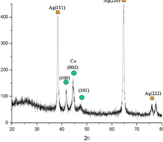
Figure 1 show the XRD patterns of the target after thermal treatment. Only ZrTiO4, ZnAl2O4 and
residual ZrO2 was detected (Fig.2.1.a). The microstructure of target ZAT1and ZAT2 were primarily
composed of granular ZnAl2O4 crystal about (2 µm) and submicro prismatical ZrTiO4 crystal. In
order to investigate the relationship between laser fluence and nanoparticles composition, phase transition of microstructure of ZAT1and ZAT2 target under different laser fluence was examined. As shown in Fig.2.2 show surface evolution. It was observed that the surface evolution changes from relief structure to smooth structure while the applied laser fluence increases. Figure 2.3 shows the surface element mapping for ZAT1under 0.34 J/cm2. Mapping result disclosed prominent area contains Zr-rich and concave area has Zn-rich. It means that Zr-rich area was subjected to a lower ablation rate but a higher ablation rate was applied at Zn-rich area under 0.34 J/cm2 fluence. That is the reason why the generated fine nanoparticles contain higher Zn content and lower Zr content. In addition, Al element distribution is similar to Zn element, and Ti element could be found at the whole area. As increasing the fluence over threshold value, all oxide compounds or elements could be laser-ablated to generate nanoparticles with homologous microstructure and compositions other than Zn content.
2.3.2 Morphology of ablated nanoparticle
Prior to laser ablation for multiphase oxide, single oxide compound was first studied. I was found that ZrO2 has a higher threshold energy density of 3~5 J/cm2 and TiO2 is 1~1.5 J/cm2. The
nanoparticles with an average particle size of 20~40 nm under threshold fluence can be obtained by laser ablation process. On the other hand, both ZnO and Al2O3 have lower threshold of 0.4 - 0.6
J/cm2, but 5~20 nm finer nanoparticles were generated. According to the ablation model for single oxide ceramic, it reveals that many parameters such as bonding strength, absorption property and wavelength will influence the threshold energy density. Therefore, for multiphase oxide compound, it would become more complicated because of different bonding strength or threshold fluence. According to laser-ablation experiment for ZAT1 and ZAT2, 0.34 J/cm2 fluence only obtains
ablation rate of 0.3~0.7µg/shot at air atmosphere that was below threshold . As increasing the fluence to 1 J/cm2 and 4 J/cm2, the ablation rate of 1.9~3.2 µg/shot and 2.3~3.4µg/shot, respectively, can be reached that is near the saturated ablation condition. Therefore, three fluences of 0.34, 1 and 4 J/cm2 would be used for the laser ablation process .
Nanoparticles produced by 0.34~4 J/cm2 laser fluence at air atmosphere show amorphous-like structure [Fig. 2.1b and c] and exhibit two kind of particle size distribution with fine nanoparticles of 5~20 nm (70~90%) and large spherical nanoparticles of 40~100 nm (10~30%) as shown in Fig.2.4.a,b,c). While stronger laser fluence was applied, the number of large spherical particles becomes more (is increased). According to static method, average particle size of 8.2 nm, 10.7 nm and 11.6 nm was obtained under 0.34, 1 and 4 J/cm2 of laser fluence, respectively. The influence of laser power on the crystallization evolution of nanoparticle is also observed in Fig. 2.5 for ZAT1 and ZAT2 where both exhibit different phase evolution. However, The phase crystallization increases with a stronger fluence. The electron diffraction pattern shows better crystalline particle for high laser power (1 J/cm2) but lower laser power gives amorphous-like particle. These results may explain both gas and liquid phases existed in the ablated agglomeration. The higher laser power digs out larger particle with liquid phase on its surface. Good crystallization is also found for these large particles. When the low laser power is applied, the only excited particle is gas-like phase and will be consolidated into amorphous phase because of the quench effect of flow gas or atmosphere. Therefore, fine particle with amorphous phase is found (see Fig.2.4.b). The amorphous fine particle can be crystallized by electron beam during TEM observation or temperature treatment. Therefore, it can be summarized. The higher laser power gives larger particles with wide size distribution, while the lower ones provides fine particles with narrow size distribution. Compromise between laser power and temperature treatment can produce fine particle with narrow size distribution and good crystallization.
As the nanoparticles were synthesized in nitrogen atmospheres, the nanoparticles in Fig. 2.4.d appeared wilder particle distribution than that synthesized in air atmospheres. On the other hand, in
oxygen atmospheres, some hollow nanoparticles as shown in Fig.2.4.e.f.appear in this condition. Gas flow to bring out particle from surface changes ablation rate. Increasing flow rate carries out more particles and makes the surrounding environment easier for the following particle generation The ablation rate varies with the change of atmosphere condition because gas flow to bring out particle from surface occurs during laser ablation and changes with atmosphere condition. It was found that oxygen has a larger density and viscosity (1.43×10⁻³g/cm3 and 2.08×10⁻⁵g/s cm, Poise) ‧ than air (1.32×10⁻³g/cm3 and 1.86×10⁻⁵g/s cm, Poise) and nitrogen (1.25×10‧ -3g/cm3 and 1.79×10⁻⁵g/s cm, Poise). Therefore, in oxygen atmospheres, the laser‧ -induced plume become small due to the short mean free path because of high viscosity and thus it causes more probability for the laser beam to irradiate the agglomerated nanoparticles to generate large hollow nanoparticles
2.3.3 Phase separation of ablated nanoparticle
Composition of the generated nanoparticles from both targets of ZAT1 and ZAT2 were inspected by TEM and EDS analysis based on a normalized molar ratio of atoms with Zr+Ti+Zn+Al=100%. Fig.2.6 show element evolution of three types of nanoparticles under different fluences in air atmosphere. Both ZAT1 target have similar result as ZAT2, but element show more close value under 1 and 4 J/cm2 laser fluence for fine nanoparticles. For fine nanoparticles (5~20nm) generated from ZAT2 target, it was found that Zn content decreases but Zr content increases while the laser fluence rises. In addition, both Al and Ti content present similar trend to Zr but littler irregular. However, in the case of large spherical nanoparticles (40~100nm), the Zn content was apparently decreased but the others increase with an increase of laser fluence. It was believed that because Zn content was easier evaporated into gas phase than the others as the fine nanoparticles were condensed from vapor phase, more Zn content would be trapped. In addition, as the larger crystalline particles were formed, the EDS shows that it was primarily composed of Zr over 70 % with little Zn.
26
2.3.4 Far-infrared ray emissivity characteristion
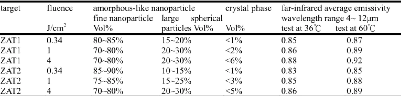
The far-infrared ray emissivity characterization of nanoparticles based on ZrTiO4--ZnAl2O4 system was investigated with black body furnace as a reference of 1. Table 2.1 summarized the average emissivity of more than 80﹪fine nanoparticles (wavelength in the range of 4 to 12 µm) under different condition. The average emissivity were as function of the synthesized nanoparticle size, composition and formation phase and varies upward with increasing large spherical particles and crystal phase ratio .
2.4. Summary
Laser ablation is an important and useful method for oxide nanopartcles with single or multiphase. Surface of target will be annealed by laser power and presents nearly constant ablation rate after several shots. Higher laser power creates larger particle with good crystallization, while lower ones gives fine and amorphous particles. Multiphase target suffers from phase separation due to the different laser absorption ability. Modification of target composition may relieve this problem.
27
2.5 References
[2.1]M. Choi, J. Nanoparticle Res., 3 (2001) 201-211 [2.2]K. Landfester, Adv. Mater., 13 (2001) 765-768
[2.3]Y. C. Kang, S. B. Park and Y. W. Kang, Nanostructured Mater. 5 (1995) 771-791 [2.4]Z. Paszti, G. Peto, Z. E. Horvath and A. Karacs, Appl. Surface Sci., 168 (2000) 114-117
[2.5]T. Sasaki, S. Terauchi, N. Koshizaki and H. Umehara, Appl. Surface Sci., 127-129 (1998) 398-402
[2.6]K. Tanaka and D. Sonobe, Appl. Surface Sci., 140 (1999) 138-143 [2.7]H. Takashima, Yogyo-Kyokai-Shi 89,[12](1981)655-660
[2.8]H. Takashima, K. Matsubara, Y. Nishimura and E. Kato, Yogyo-Kyokai-Shi 90,[7](1982)373-379
28
Fig.2.1.a. XRD pattern of crstal phases of ZAT1 target after thermal treatment. b. XRD pattern of nanoparticles produced by 4 J/cm2 laser fluence at air atmospheres.c. XRD pattern of nanoparticles produced by 0.34 J/cm2 laser fluence at air atmospheres.
29
30
Fig.2.4.a.b.c. Nanoparticles produced by 0.34~4 J/cm2 laser fluence irradiating at air atmosphere. 2.4.d . nanoparticles synthesized at nitrogen atmospheres. 2.4..e&f. nanoparticles synthesized at oxygen atmospheres.
31
Fig.2.5. The evolution of TEM diffraction pattren of nanoparticles of ZAT1 and ZAT2 under different fluence
32
Fig.2.6. element evolution of three type nanoparticles under different fluence and air atmosphere
33
.
target fluence amorphous-like nanoparticle crystal phase far-infrared average emissivity J/cm2 fine nanoparticleVol% large spherical particles Vol% Vol% wavelength range 4~ 12µm test at 36 test at 60℃ ℃
ZAT1 0.34 80~85% 15~20% <1% 0.85 0.87 ZAT1 1 70~80% 20~30% <2% 0.86 0.89 ZAT1 4 70~80% 20~30% <6% 0.88 0.92 ZAT2 0.34 85~90% 10~15% <1% 0.83 0.85 ZAT2 1 75~85% 15~25% <3% 0.85 0.88 ZAT2 4 70~80% 20~30% <5% 0.86 0.89
Table 2.1 summarized the average emissivity of the nanoparticles that were more than 80 ﹪(wavelength range from 4 to 12µm) under different condition.
34
Chapter 3
Nanoscaled TiO
2/Ag catalyst and photodecomposition characteristic
3.1 Introduction
The photodecomposition of various pollutants by TiO2 has been demonstrated to be efficient under ultraviolet light [3.1-3.16]. The photocatalytic activity of TiO2 can also be enhanced by modifying its surface with noble metals and metal oxides [3.8]. These photocatalysts are utilized in many approaches. For example, TiO2 photocatalysts anchored on supporting materials with large surface areas have been developed to eliminate the shortcomings of the filtration and the suspension of fine photocatalyst particles [3.5]. TiO2 photocatalysts anchored on various substrates were prepared using a pasting treatment, an ionized cluster beam (ICB) method or a sol–gel method [3.6]. The sol-gel method is frequently adopted to prepare TiO2 thin films on supported substrates [3.1-3.7, 3.10-3.13]. However, heat treatment may cause a phase transition of TiO2 and reduce the photocatalytic activity [3.5].
This study proposes the anchoring of well-dispersed nano TiO2 on a metal carrier using a binder-free, low temperature process. Well-dispersed nano TiO2 deposited on a branch-like silver (Ag) carrier, called “nano-TiO2/Ag catalyst” was synthesized here to overcome the aforementioned shortcomings. This study discusses the preparation, morphology and reaction kinetics of photocatalytic activity of nano-TiO2/Ag catalyst.
3.2 Experimental
An Ag carrier was prepared based on the reaction, 2Ag+ + CuÆ2Ag + Cu+2. The net redox potential of the reaction is 0.5V indicating that the reaction occurs spontaneously. In a pretest, the formation of the branch-like Ag carrier was favored in the acidic solution at high concentration [17]. Bulk copper (Cu) was placed in AgNO3 solution at a ratio of Cu: AgNO3: water =5: 3: 100 (wt %), to yield Ag particles. Nitric acid was added to give the solution a pH of 3. The solution temperature was set to 25 , which℃ was maintained for 2 hrs. Then, the precipitate was rinsed with D.I water to remove residues.
Secondly, an appropriate amount of TiO2 particles (P25, Degussa) was placed in the solution at various pH values, obtained by adjusting the amount of NH3(aq) or nitric acid
35
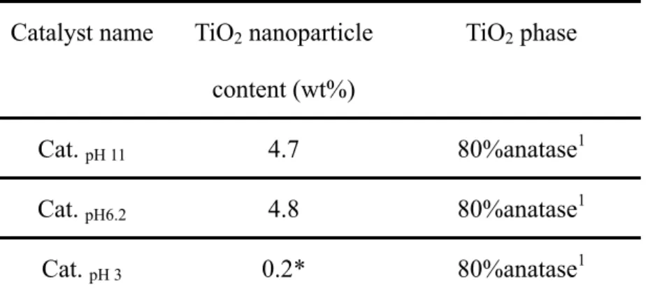
added. The solution was treated ultrasonically for 90mins. No dispersing agent was added to the solution. The experimental design was such that 5 wt % of TiO2 was mixed with Ag carrier at various pH conditions. A critical coverage ratio of TiO2 of approximately 5% was identified: exceeding this dosage of TiO2 may result in aggregation under all test pH conditions. The mixture was stirred for 30 mins to increase the number of opportunities for contact between nano TiO2 particles and Ag carriers. Finally, a composite of nano TiO2 particles and Ag carrier was synthesized by washing, filtering and drying, in that order. Table 3.1 presents the characteristics of nano-TiO2/Ag catalyst used in this study.
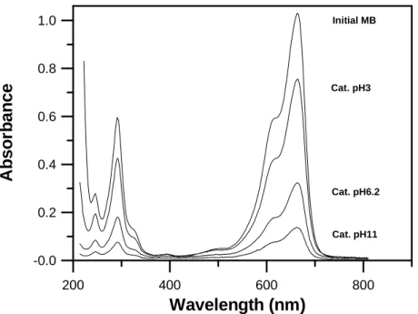
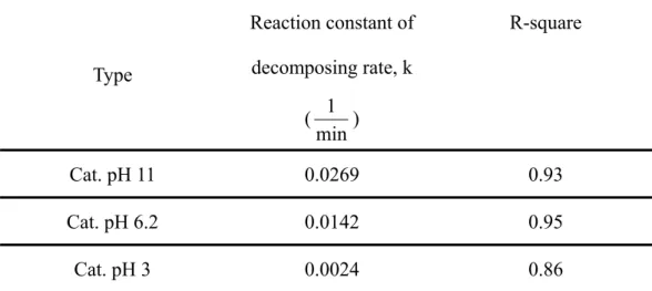
Methylene blue (MB) is a representative dye that is commonly adopted to evaluate the catalytic activity of a catalyst. The test conditions were as follow; 1g of catalyst, 30 ml of 100 ppm MB solution, UV light with a wavelength of 254 nm and an illumination intensity of 4mW/cm2. The UV lamp was placed 6cm above the test sample. The mixture (MB and catalyst) was stirred gently while being irradiated. A centrifuge was used to separate the mixture after irradiation had been completed. The absorption of the MB supernatant was then determined using a spectrophotometer (Unico UV2102). A blank experiment (without a catalyst) was also performed; the results indicated that irradiation did not significantly change MB absorbance. The photocatalytic activity was defined as
100% C C C η initial n irradiatio initial− × =
where Cinitial and Cirradiation are the absorbance of MB before and after irradiation. The morphology of the catalysts is observed by field emission-scanning electron microscopy (FE-SEM, LEO, 1530).
3.3 Results and discussion
The SEM images of the Ag nanoparticles are shown in Figure 3.1. Figure 3.1a~3.1d shows the typical SEM images of the product obtained by self-reducing the solution with concentration
from 0.1wt% to 1.5wt% AgNO3. It is apparent that Ag nanoparticles display dendritic growth
while concentration>0.5wt%. We believe that the excess of silver in the solution may be favorable for the aggregation and growth into the dendritic structures of the Ag cluster. It is found
that the concentration of AgNO3 plays a significant role in the formation and growth of the silver
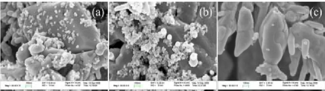
![Fig. 6.3 Cyclic-voltammetry analysis by altering [Co 2+ ]/ [Ag + ] ratio 50, 100, 210](https://thumb-ap.123doks.com/thumbv2/9libinfo/8752776.206229/94.892.106.713.130.1091/fig-cyclic-voltammetry-analysis-altering-ag-ratio.webp)