國 立 交 通 大 學
電子工程學系 電子研究所
博 士 論 文
新穎反轉式及無接面多閘極多晶矽奈米線薄膜電晶體特性與應
用的探討
An Investigation on the Characteristics and Applications of
Novel Multiple-Gated Inversion-Mode and Junctionless
Polycrystalline Silicon Nanowire Thin-Film Transistors
研 究 生:林哲民
指導教授:林 鴻 志 博士
黃 調 元 博士
新穎反轉式及無接面多閘極多晶矽奈米線薄膜電晶體特性與應
用的探討
An Investigation on the Characteristics and Applications of Novel
Multiple-Gated Inversion-Mode and Junctionless Polycrystalline
Silicon Nanowire Thin-Film Transistors
研 究 生:林哲民
Student:Hsing-Hui Hsu
指導教授:林鴻志博士
Advisors:Dr. Horng-Chih Lin
黃調元博士
Dr. Tiao-Yuan Huang
國 立 交 通 大 學
電子工程學系 電子研究所博士班
博 士 論 文
A Dissertation
Submitted to Department of Electronics Engineering &
Institute of Electronics
College of Electrical and Computer Engineering
National Chiao Tung University
In Partial Fulfillment of the Requirements
for the Degree of
Doctor of Philosophy
in
Electronics Engineering
March 2012
Hsinchu, Taiwan, Republic of China
中 華 民 國 一百零一 年三月
新穎反轉式及無接面多閘極多晶矽奈米線薄膜電晶體
特性與應用的探討
研究生:林哲民
指導教授: 林鴻志 博士 黃調元 博士 國立交通大學 電子工程學系 電子研究所摘要
本篇論文研究獨立雙閘極(independent double-gated)多晶矽奈米線薄膜電晶 體操作於低汲極(drain)偏壓時,雙閘控制模式相對於單閘控制模式而言有較佳輸出 電流的主要原因。實驗數據以及理論分析結果顯示,當多晶矽奈米線元件操作於 雙閘模式控制之下,對於通道中晶粒邊界與缺陷所造成之位能障(grain-boundary potential barrier)具有較佳的調控能力,因而可獲得相較單閘操作下為佳的元件特 性。 另一方面,本研究也探討將獨立雙閘極機制應用於 SONOS 記憶體元件中的 可能性。由於獨立雙閘極 SONOS 記憶體元件具有兩個可以獨立操作的閘極,所以 有兩種讀取模式可供選擇。論文中分析了兩種不同讀取模式對感測窗口大小 (memory window)特性的影響。本論文製作的元件採用的雙閘極介電層分別為二氧 化矽以及二氧化矽-氮化矽-二氧化矽堆疊層。當選用具二氧化矽-氮化矽-二氧化矽 堆疊層為閘介電層之閘極當驅動閘極(driving gate)時,SONOS 記憶體元件具有比 較大的感測窗口,但是,其大小與施加於輔助閘極的偏壓無關。根據這些分析,本研究提出了幾種以無摻雜或重摻雜矽薄膜為通道且具獨立雙閘極之先進非揮發 性記憶體結構,其主要特徵為具有一共用輔助閘來增進性能。
除 了 獨 立 雙 閘 極 多 晶 矽 奈 米 線 薄 膜 電 晶 體 外 , 運 用 全 包 覆 式 閘 極 (gate-all-around)無接面(junctionless)多晶矽奈米線薄膜電晶體的電流-電壓(I-V)量 測,我們也發展了ㄧ個可用於檢測重磷摻雜多晶矽奈米線通道的活化摻雜濃度 (active doping concentration)、遷移率(mobility)及分布於閘極介電層與通道間的表 面二氧化矽閘極介電層電荷密度(interface oxide charge density)的量測方法。利用此 方法獲得的重磷摻雜多晶矽奈米線通道特性分析結果與實施於帄面無接面薄膜電 晶體的電容-電壓(C-V)量測分析結果相當ㄧ致。相較於對重磷摻雜多晶矽塊材進行 霍爾量測(Hall measurement)所獲得的分析結果,上述兩個方法皆顯示較低的活化 摻雜濃度以及大量負的表面二氧化矽閘極介電層電荷密度。其主要原因推估為磷 於二氧化矽閘介電層與多晶矽通道間介面的偏析(segregation)現象。 此外,考慮到無接面場效電晶體的實際應用,本研究也發展了一個理論模 型,可用於描述雙閘極無接面場效電晶體的臨界電壓(threshold voltage)與次臨界電 流(subthreshold current)。其計算結果顯示,此模型可以準確的描述雙閘極無接面場 效電晶體導通通道長度從 100 nm 微縮至 22 nm 時,元件呈現的臨界電壓下降效應 (threshold voltage roll-off effect) 。
除了探討一般的無接面場效電晶體,考量蕭特基位障(Schottky-barrier)電晶體 於非揮發性記體元件的應用潛力,本研究也提出了一種新穎的非對稱蕭特基位障 電晶體。此非對稱元件具備了蕭特基位障於源極(source)端,然而,其導通通道與 汲極皆為重 n 型摻雜。計算結果顯示,其非對稱的特性使得此蕭特基位障電晶體 顯示出單極(unipolar)的傳輸特性以及低的漏電流,但是其位於源極端的蕭特基位 障也劣化了元件的輸出電流以及操作於擬次界區(pseudo-subthreshold region)的次 臨界擺幅(subthreshold swing)。而此次臨界擺幅的劣化可藉由薄化導通通道以及閘
極介電層來獲得改善。除此之外,本研究也提出了修正的微縮長度(scaling length)
“λ”概念,來描述導通通道以及閘極介電層的厚度對位於擬次界區的次臨界擺
幅所產生的影響。
最後,本論文在全包覆式閘極反轉模式 (inversion-mode)多晶矽奈米線元件 常溫量測中發現獨特的低於 60 mV/dec 的次臨界擺幅現象。其主要原因推估與下面 兩項描述相關。第一、trap-assisted band to band tunneling (BTBT) current 於汲極端 產生了大量的電洞,其中部分被擷取於晶粒邊界之缺陷所造成之能階狀態中。第 二、後續當元件操作於次臨界區(subthreshold region)時,擷取的電洞被中和。然而, 我們的量測數據顯示,當元件通道長度逐漸微縮或者包覆式閘極遭單閘取代時, 此獨特現象將逐漸消失。 關鍵字:奈米線, 獨立雙閘極, 全包覆式閘極, 多晶矽, 薄膜電晶體, SONOS, 無接 面, 蕭特基位障, SONOS, 低於 60 mV/dec 的次臨界擺幅。
An Investigation on the Characteristics and
Applications of Novel Multiple-Gated
Inversion-Mode and Junctionless Polycrystalline
Silicon Nanowire Thin-Film Transistors
Student: Zer-Ming Lin Advisors: Dr. Horng-Chih Lin Dr. Tiao-Yuan Huang
Department of Electronics Engineering & Institute of Electronics National Chiao-Tung University
Abstract
In this dissertation, we study the characteristics of independent double-gated (IDG) polycrystalline silicon (poly-Si) nanowire (NW) thin-film transistors (TFTs) with focus on the physical mechanism responsible for the superior output current under double-gated (DG) mode of operation over that under single-gated (SG) mode at a small drain voltage. The experimental data and theoretical analysis identify that the root cause is related to the more efficient modulation of grain boundary barrier height of poly-Si channels under DG mode of operation.
On the other hand, the feasibility of applying such IDG scheme to silicon–oxide–nitride–oxide–silicon (SONOS) flash memory is also explored. Two
different read modes can be adopted in such IDG poly-Si NW SONOS device with the two independent control gates. Special attention is paid to the analysis of memory window under different read modes. The fabricated device has oxide and oxide-nitride-oxide (ONO) stack as dielectrics for the two independent gates, respectively. Our analysis and experimental data show that a larger memory window is obtained when the gate with ONO stack as dielectrics is used as the driving gate. Moreover, the memory window of this mode is essentially independent of the bias applied to the auxiliary gate. Based on this finding, several novel IDG Flash structures with undoped or heavily doped silicon channels and a common auxiliary gate are proposed.
Next, based on the measured I-V characteristics of gate-all-around (GAA) poly-Si NW junctionless (J-less) TFTs, we develop a methodology capable of extracting the values of active doping concentration, mobility, and interface fixed charge density of the in situ phosphorous-doped poly-Si NW channel. The experimental results show lower
value of active doping concentration as compared to that obtained from Hall measurements performed on blanket thin films. Moreover, a highly negative interface oxide fixed charge density is found as well. These measured properties of the heavily doped poly-Si NWs are compared with the results of C-V measurements performed on planar J-less transistors with an ultra-thin channel. Close agreement is obtained between
these two schemes. Segregation of phosphorous at gate oxide/NW interface is postulated to be the responsible mechanism for the observed phenomena.
In this dissertaton, we also develop an analytical model of threshold voltage (Vth)
and subthreshold current for DG J-less transistors by solving the two-dimensional Poisson’s equation. The Vth roll-off effect of DG J-less transistors with channel length
from 100 to 22 nm can be well described through the proposed model as the channel thickness is thinned to 8 nm.
In addition, we also propose a new asymmetric n-channel SB transistor (ASSBT) which features SB only on the source side, while the channel and drain are both n+ doped. Our calculation results show that such a device exhibits unipolar behavior and low off-state leakage current owing to the elimination of SB originally presenting on the drain side. However, aggravated subthreshold swing (SS) in the pseudo-subthreshold region and degraded output current are found because of the SB source. Based on the calculation results, the aggravated SS can be improved by thinning the thickness of silicon channel or gate oxide. A modified form of scaling length (λ) concept is introduced to describe the impacts of structural parameters and gate configurations on the SS characteristics in the pseudo-subthreshold region.
mV/dec SS found in GAA inversion-mode (IM) poly-Si NW TFTs at room temperature. The responsible physical mechanism related to the trapping of excessive holes generated by the high trap-assisted band-to-band tunneling (BTBT) current and later recombination of these trapped holes when operating in the subthreshold regime is suggested. Moreover, the experimental data also indicate that such an unexpected phenomenon is relieved or even negligible with the decrease of channel length or the replacement of GAA configuration by a single-gated one.
Keywords: nanowire (NW), independent double-gated (IDG), gate-all-around (GAA),
polycrystalline silicon (Poly-Si), thin-film transistor (TFT), silicon-oxide-nitride-oxide-silicon (SONOS), junctionless (J-less), Schottky-barrier (SB), sub-60 mV/dec SS.
誌謝
寫下致謝的同時也同時代表了博士求學生涯的結束,另一個嶄新階段的開 始,在結束這個階段的同時,首先我要感謝林鴻志教授與黃調元教授,兩位老師 博學多聞且不倦的指導,尤其兩位老師對我發表的每一篇論文皆不倦的ㄧ個字一 個字耐心的修正,學生對此銘記於心。另外,兩位老師嚴謹的研究態度,創新研 發的精神實為學生一生的典範。 接下來,我要感謝實驗室所有學弟妹們,包括博士班一起奮鬥過的夥伴,徐 博、大師、馬腳、阿毛、子儀、嘉文、阿莫、克慧等,謝謝你們不只在實驗上幫 忙,也包括生活上大小事歡樂與淚水的分享。另外也謝謝各位碩士班學弟妹,尤 其是跟我同甘共苦過的歷樺、澎澎、村長,謝謝你們在我博士求學生涯最後的階 段,帶給我這麼多笑聲。 最後,我要謝謝我的家人,老爸、老媽、臭弟,這本論文的完成是你們的堅 持與努力,謝謝你們給我最有力的支持與後盾,才有論文的完成。然後是我細心 體貼的老婆依娟,博士生涯最後兩年的階段,謝謝你陪著我幾乎在每一個週末依 然是在建 model,寫文章,沒有你的陪伴,我無法走過每一個高低潮。 僅以此論文獻給摯愛的家人、朋友與敬重的師長。 林 哲 民 誌於風城交大 2012 年 3 月Contents
Abstract (Chinese) ... i
Abstract (English) ... iv
Contents…. ... ix
Table Captions ... xii
Figure Captions ... xiii
Chapter 1 Introduction ... 1
1.1 Overview of Nanowire Technology ... 1
1.1.1 Bottom-up and Top-down Approaches ... 2
1.1.2 Approaches Developed by Our Group ... 4
1.2 Overview of Multiple-Gated Devices ... 6
1.3 Overview of Junctionless (J-less) Nanowire Transistors ... 11
1.4 Overview of Schottky-barrier (SB) MOSFETs ... 16
1.5 Overview of Devices with Sub-60 mV/dec Subthreshold Swing (SS)………..21
1.6 Motivation ... 24
1.7 Thesis Organization ... 26
References… ... 29
Chapter 2 Performance Enhancement of Poly-Si Nanowire (NW)
Transistors with Independent Double-gated (IDG)
Configuration ... 56
2.1 Introduction ... 56
2.2 Experiments .………..57
2.3 Performance Enhancement under DG Control………...59
2.4 Experimental Analysis on the Double-gate Modulated Barrier Lowering ... 60
2.5 Theoretical Analysis………...62
2.6 Summary………...64
References…. ... 65
Chapter 3 Read Characteristics of Independent Double-Gated (IDG)
Poly-Si Nanowire SONOS Devices ………...75
3.2 Device Structure ... 78
3.3 Effects of Auxiliary Gate Bias on Vth of the IDG Devices ... 78
3.4 Memory Window under Two Read Models in IDG Devices………80
3.5 Experimental Verification and Discussion ... 83
3.6 Innovative IDG SONOS Devices………...86
3.7 Summary………...89
References…. ... 90
Chapter 4 A New Methodology for Probing the Electrical
Characteristics of Heavily Phosphorous-Doped Poly-Si
Nanowires with Gated-All-Around (GAA) Junctionless
(J-less) Structure ... 104
4.1 Introduction ... 104
4.2 Device Fabrication ... 106
4.3 Impacts of the Cross-sectional Area of the NWs ... 107
4.4 Theoretical Background………..109
4.5 Experimental Verification and Discussion ... 111
4.6 Comparisons with the Results of SIMS and HALL Measurements…………115
4.7 Further Verification by C-V Measurements on N-channel Planar J-less Transistor…….………115
4.8 Summary………..119
References…. ... 121
Chapter 5 Analytical Model of Threshold Voltage and Subthrshold
Current
for
Fully-Depleted
Double-gated
(DG)
Junctionless (J-less) Transistors ... 141
5.1 Introduction ... 141
5.2 Solution of 2-D Poisson’s Equation ... 142
5.3 Subthreshold Current and Swing ... 146
5.4 Threshold Voltage Roll-off……… .148
5.5 Summary………..153
References…. ... 154
Chapter 6 Characteristics of N-type Asymmetric Schottky-barrier
Transistors (ASSBTs) with Silicided Schottky-barrier
Source and Heavily N-type Doped Channel and Drain
... ..166
6.1 Introduction ... 166
6.2 Subthreshold Characteristics of ASSBT ... 168
6.3 Deep Insight into the Suthreshold Characteristics of ASSBT ... 169
6.4 Impacts of tch and tox on the Transfer Characteristics of ASSBTs…………...171
6.5 A New Inverter Scheme Built by Dual Workfunction (DW) DG N- and P-type ASSBTs………...174
6.6 Summary………..176
References…. ... 178
Chapter 7 Mechanisms for Sub-60 mV/dec Subthreshold Swing (SS)
Found
in
Gate-All-Around
Polycrystalline
Silicon
Nanowire Thin-Film Transistors (TFTs) ... 198
7.1 Introduction ... 198
7.2 Device Fabrication ... 200
7.3 Abnormal Subthreshold Characteristics of the GAA Poly-Si NW Transistors...201
7.4 Proposed Mechanisms and Discussion………....203
7.5 Impacts of Channel Length and Gate Configuration on the Abnormal Vth and SS. ………..205
7.6 Summary………..207
References………..209
Chapter 8 Conclusions and Future Prospects ... 224
8.1 Conclusions ... 224
8.2 Future Prospects ... 228
8.2.1 Three-Dimensional Integration of J-less Poly-Si NWTFTs and NVMs……… ... 228
8.2.2 Metal-Oxide-Metal Field Effect Transistors (MOMFETs) ... 229
References… ... 231
Vita……….. ... 233
Table Captions
Chapter 4
Table 4-I Detailed parameters applied to a two-dimensional TCAD tool for the calculation of electric potential distributions shown in Fig. 4-9. ……....123 Table 4-II Results of SIMS, Hall measurements and the proposed methodology for in
situ phosphorous-doped poly-Si NWs. . ... ……...124 Table 4-III Results of extracted active doping concentration, interface fixed oxide charge density, oxide thickness, and flatband voltages from planar J-less transistors with channel thickness of 8, 10, 12 nm, respectively, by C-V measurements. . ... ……...125
Chapter 6
Table 6-I Major parameters of SSBT and ASSBT used in simulations. ... 181 Table 6-II Major parameters of the proposed new inverter (Fig. 6-14(a)) used in
Figure Captions
Chapter 1
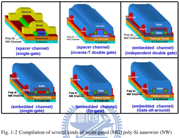
Fig. 1-1 Growth mechanism of silicon nanowires by means of vapor-liquid-solid (VLS) approach [1.14]. ……….45 Fig. 1-2 Compilation of several kinds of multi-gated (MG) poly-Si nanowire (NW)
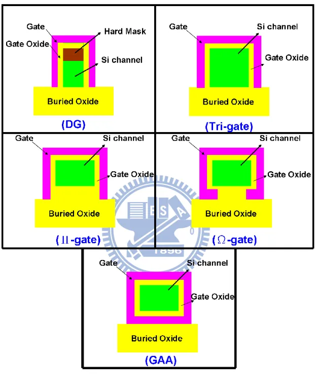
thin-film-transistors (TFTs) developed by our group. ... 46 Fig. 1-3 Schematic cross-section of several kinds of multi-gated (MG) FinFETs, including DG, Tri-gate, Π-gate, Ω-gate, and GAA. ………...47 Fig. 1-4 Distribution of doping concentration in fin by (a) low-energy vertical
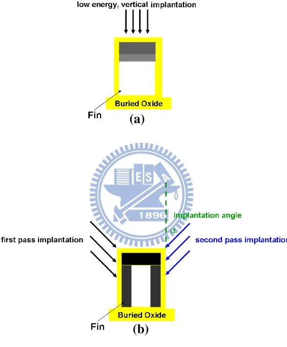
implantation and (b) two-pass tilted implantations. The darker region means heavier doping concentration. (c) Different dopant loss mechanisms indicated by the dash arrowheads in the tilted implantation [1.67]. (d) Restriction of implantation angle owing to the shadowing issue due to the physical height of adjacent resist. ………48 Fig. 1-5 Comparison of ID-VG characteristics of (a) n-type inversion-mode (IM) and (b)
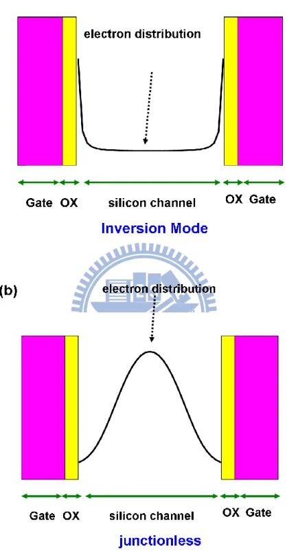
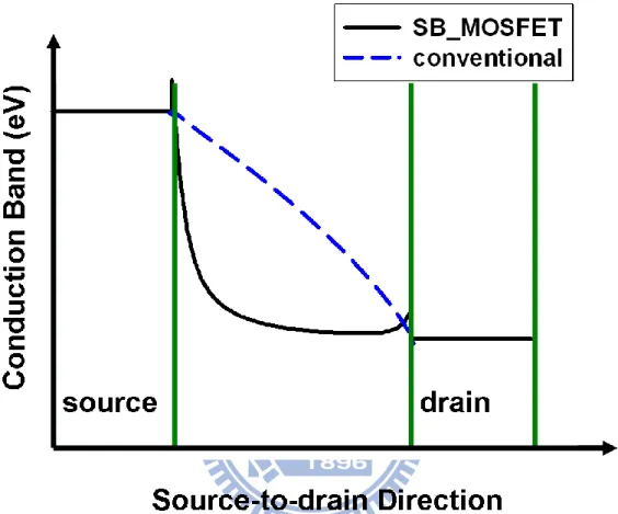
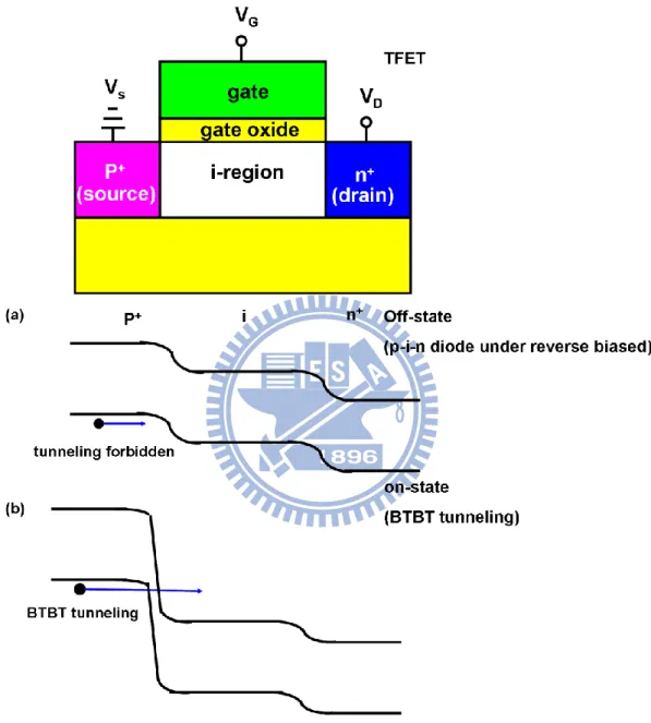
n-type junctionless (J-less) NW transistors [1.79]. ……. ... 50 Fig. 1-6 Distribution of electron density in (a) DG n-type inversion-mode (IM) and (b) DG n-type junctionless (J-less) NW transistors along the direction perpendicular the carrier transport. ... 51 Fig. 1-7 Comparison of conduction band energy of SB and conventional MOSFETs. The particular abrupt drop near the source of the SB MOSFETs results in the efficient generation of hot carriers. ………52 Fig. 1-8 Band diagrams of an n-channel TFET in (a) off and (b) on state,
respectively. ………53 Fig. 1-9 Band diagrams of an n-channel I-MOS in (a) off and (b) on state, respectively. ... .54 Fig. 1-10 Typical latch-up phenomenon found in SOI devices. ... 55
Chapter 2
Fig. 2-1 (a) Stereo view as well as cross-sectional TEM image and (b) top view of the n-type IDG poly-Si NW TFTs investigated in this chapter, featuring two independently-biased gates and rectangular poly-Si NWs. ……… .67 Fig. 2-2 (a)~(d) Key steps of fabrication flow of the IDG poly-Si NW TFTs investigated in this chapter. ………...68 Fig. 2-3 (a) ID-VG characteristic of the investigated IDG poly-Si NW TFT, featuring
m under SG-1, SG-2, and DG modes of operation. (b) Comparison of the output characteristic under DG mode of operation with the sum of those under SG-1 and SG-2 modes of operation. ………...69 Fig. 2-4 Extracted VB as a function of gate voltage for the device characterized in Fig.
2-3. The inset shows some of the log(ID) vs. temperature (T) curves for
extracting VB. DG mode shows reduced VB as compared with the SG
mod. ………..70 Fig. 2-5 Simplified 2D schematic illustration of the device applied in 2D TCAD simulation, featuring poly-Si channel thickness of 20 nm, gate oxide of 14 nm as well as gate length of 5um and bamboolike structure corresponding to the granular channel of IDG poly-Si NW TFT. ………...71 Fig. 2-6 The simulated (a) ID-VG and (b) ID-VD characteristics of the IDG poly-Si NW
TFT under DG and SG modes of operation. Excellent agreements with those from experimental measurements shown in Fig. 2-3 are obtained. ………...72 Fig. 2-7 The simulated VB values at y = 1, 3, and 5 nm with simulated ID-VG and ID-VD
characteristics shown in Fig. 2-6. ... 73 Fig. 2-8 Comparisons of experimental and simulated TEF under DG and SG modes of operation. ... 74
Chapter 3
Fig. 3-1 (a) Stereo view as well as the cross-sectional TEM image and (b) top view of the n-type IDG poly-Si NW SONOS TFT characterized in Chapter 3. ONO and oxide are used as the gate dielectrics of the first and second gates, respectively. ………...93 Fig. 3-2 Schematic structure of a typical n-type IDG device for analysis in Sec. 3-3. .. 94 Fig. 3-3 Vth(dri)−VG(con) characteristics of a typical n-type IDG device. Three distinctly
different regions corresponding to various channel surface conditions of the control gate side can be defined. .. ………95 Fig. 3-4 Schematic structure of the n-type IDG devices with extra negative charges incorporated in the gate oxide of G1. ………...96 Fig. 3-5 (a) Vth(dri) versus VG(con) characteristics and (b) memory window versus VG(con)
read in mode I with or without extra charges incorporated. ... 97 Fig. 3-6 (a) Vth(dri) versus VG(con) characteristics and (b) memory window versus VG(con)
read in mode II with or without extra charges incorporated. ... 98 Fig. 3-7 Measured transfer characteristics of the programmed (dotted lines) and
erased (solid lines) states in the IDG poly-Si NW SONOS TFT under (a) mode I and (b) mode II. ... 99
Fig. 3-8 Memory window as a function of control-gate bias read in modes I and II. The dash and solid lines refer to calculated results for modes I and II, respectively, and the circle and square symbols are the extracted results from the transfer characteristics shown in Figs. 3-7(a) and (b), respectively. ... 100 Fig. 3-9 Two-dimensional schematic structure of the n-type IDG poly-Si NW SONOS device, including detailed device parameters applied in the calculation. ... 101 Fig. 3-10 (a) Proposed flash structure consisted of a series of IDG SONOS cell devices and a common control gate. (b) Previous structure consisted of a series string of IDG SONOS cell devices. Each cell has its own control gate. ………102 Fig. 3-11 A series of (a) IDG J-less SONOS cell devices and (b) three-dimensional IDG
J-less SONOS cell devices with vertical channel. Both of them feature homogeneous and heavy doping concentration across source, channel, and drain. . ... 103
Chapter 4
Fig. 4-1 (a)~(f) Key steps of the fabrication flow of the GAA poly-Si NW J-less transistors investigated in this chapter. ……… 126 Fig. 4-2 (a) Top view and (b) cross-sectional SEM image of Device 4-A. …………128 Fig. 4-3 ID-VG characteristics of Devices 4-A and -B. Device 4-B is with a much smaller
cross-sectional area of around 2312 nm2 [4.1]. . ………129 Fig. 4-4 Schematic illustration of the cross-sectional structure of the GAA J-less transistor as VG < VFB along line AA’ shown in Fig. 4-2(a). .. ………130
Fig. 4-5 Schematic illustration of the cross-sectional structure of the GAA J-less transistor as VG < VG, off along line BB’ shown in Fig. 4-2(b). . ………131
Fig. 4-6 The procedure flowchart detailing the proposed methodology for probing the active doping concentration as well as mobility, and interface fixed oxide charge density of the GAA poly-Si NW J-less transistor proposed in this chapter. . ………132 Fig. 4-7 (a) Transfer characteristics of Device 4-A measured at various VD. The device
behaves like an ungated resistor as VG is smaller than -9.1 V. (b) Gm versus VG
measured at various VD. VG, off and VFB can be precisely determined from the
plots. ………...133 Fig. 4-8 ID extracted from Fig. 4-7(a) at VG = -10 V as a function of VD. …. ……… .134
Fig. 4-9 Simulated electric potential distributions in the middle of the NW along y-axis at VD = 0.1 V and various VG. The result shown for VG = 2.88 V confirms the
flat-band condition. ... 135 Fig. 4-10 Two-dimensional schematic structure of a planar J-less transistor featuring
raised S/D. The high/low terminals are applied to gate and S/D electrodes, respectively, during C-V measurement. ... 136 Fig. 4-11 Cross-sectional TEM image of a fabricated planar J-less transistor with in situ phosphorous-doped poly-Si channel film of 10nm in thickness. ... 137 Fig. 4-12 (a) The schematic diagram as a J-less transistor is operated in PD region with effective capacitance equaling to the series connection of gate oxide capacitance (Cox) and depletion region capacitance (Cdep) and (b) The
schematic diagram of a J-less transistor with gate voltage larger than flatband voltage and effective capacitance equaling to Cox. ... 138
Fig. 4-13 The measured C-V characteristics of planar J-less transistors with channel thicknesses of 8, 10, 12 nm, respectively. ... 139 Fig. 4-14 Comparisons of the evaluated and measured C-V characteristics of planar J-less transistors with channel thickness of (a) 8, (b)10, (c)12 nm, respectively All of the results show that the theoretical calculation can well describe the experimental results shown in Fig. 4-13 in the region of VG > Vth. ... 140
Chapter 5
Fig. 5-1 Schematic diagram of the DG FD J-less transistor with P+ polysilicon gate investigated in this work. tch, tox, and Lg are the silicon channel thickness,
effective gate oxide thickness, and channel length, respectively. ND =1.5×10¹⁹
cm-3 is the homogeneous doping concentration across the source/drain and channel. ... 156 Fig. 5-2 Comparison of the analytical electric potentials and the TCAD simulation results for (a) long (Lg =100 nm) and (b) short (Lg =22 nm) channel
devices……….157 Fig. 5-3 Comparison of the analytical subthreshold currents and the TCAD simulation
results for the long-channel device (Lg = 100 nm) measured at (a) VD = 0.1 and
(b) 1 V and the short-channel device (Lg = 22 nm) measured at (c) VD = 0.1 and
(d) 1 V. ... 158 Fig. 5-4 Comparison of the analytical subthreshold swings for different channel lengths with the TCAD simulation results. ... 160 Fig. 5-5 Comparison of the analytical threshold voltages for different channel lengths with the TCAD simulation results. ... 161 Fig. 5-6 Comparison of the analytical Vth roll-off for tch = 8, 10, 12 and 15 nm with the
TCAD simulation results at VD of (a) 0.1 V and (b) 1 V. ... 162
Fig. 5-7 Mcri×ni/ND versus tch. As tch is larger than 19 nm, the DG device becomes
PD. ………..163 Fig. 5-8 Location of ymin estimated with Eq. 5-16 and TCAD simulation for devices with
tch = 8 and 15nm. Smaller ymin means a location closer to the
source. ……….164 Fig. 5-9 Comparison of transfer characteristics of transistors with tch values of 8 and 15
nm and Lg of 22 nm, operating at VD = 1 V. Note that the one with tch of 15 nm
suffers from high leakage current. ... 165
Chapter 6
Fig. 6-1 Schematic diagrams of the (a) SSBT with silicided SB S/D and (b) ASSBT with silicided SB only on the source side investigated in this work. tch = 6 nm,
tox = 0.6 nm, WF = 0.5 eV and SBH = 0.25 eV. channel doping ND = 1 × 10¹⁹
cm-3. ... 183 Fig. 6-2 Comparisons of the ID-VG characteristics of SSBT and ASSBT with channel
length of (a) 100 nm and (b) 22 nm. ... 184 Fig. 6-3 Operation regions presented in the ID-VG characteristics of an
ASSBT. ………...………..185 Fig. 6-4 (a) Electron density and (b) electric potential through the silicon channel along y direction at x = 3 nm, and (c) the potential diagram along x direction while the ASSBT is operated in region I. ... 186 Fig. 6-5 (a) Electron density and (b) electric potential through the silicon channel along y direction at x = 3 nm, and (c) the potential diagram along x direction while the ASSBT is operated in region II. ……. . ………187 Fig. 6-6 (a) Electron density and (b) electric potential through the silicon channel along y direction at x = 3 nm, and (c) the potential diagram along x direction while the ASSBT is operated in region III. ………..188 Fig. 6-7 Band diagram of the ASSBT operated in region II showing the thermionic field emission process. ……….189 Fig. 6-8 ID-VG characteristics of ASSBTs with various (a) tch and (b) tox. (c) SS versus
to x w i t h tc h a s a p a r a m e t e r f o r A S S B Ts o p e r a t e d i n r e g i o n -
II. ………..190 Fig. 6-9 The SS versus with (a) = 0 and (b) = 0.3. In (b), the data are described well by a fitting curve. ……….191 Fig. 6-10 Schematic diagram of the DG ASSBT with SBH = 0.25 eV. ... 192 Fig. 6-11 (a) The comparison of SS for SG and DG ASSBTs with various tch and tox. (b)
The SS versus for SG and DG ASSBTs with = 0.3. ………...193 Fig. 6-12 Schematic diagram of the n-type dual-workfunction (DW) DG ASSBT with SBH = 0.25 eV. ………...194 Fig. 6-13 Comparisons of the ID-VG characteristics of SG, DG, and DW DG ASSBTs
with channel length of 22 nm. ………195 Fig. 6-14 Schematic diagram of (a) the proposed new inverter built by a pair of n- and p-type DW DG ASSBTs sharing a common back-gate with workfunction of 4.5 eV and (b) the inverter proposed in the previous study [6.19]. ... 196 Fig. 6-15 (a)Vin-Vout characteristics, (b) switching current and (c) AC transient output
voltage of the proposed new inverter (Fig. 6-14(a)). ... 197
Chapter 7
Fig. 7-1 (a) 3-D schematic structure and (b) top view of the GAA poly-Si NW TFT investigated in this study. ………...211 Fig. 7-2 Cross-sectional TEM image of a fabricated GAA poly-Si NW TFT. ……….212 Fig. 7-3 (a) Transfer characteristics as well as (b) the extracted Vth and (c) SS of a GAA
poly-Si NW TFT with Lg = 5 m as a function of VD. ………...213
Fig. 7-4 (a) Transfer characteristics as well as (b) the extracted Vth and (c) SS of a GAA
poly-Si NW TFT with Lg = 5 m with different starting point of VG while fixed
VD of 3V. ……….………...………214
Fig. 7-5 ID-VG characteristics of a GAA poly-Si NW TFT with Lg = 5 m at VD = 0.1
and 2 V. The measurement first swept VG from -1 to 2 V (Forward Sweeping)
and then from 2 to -1 V (Backward Sweeping). ... 215 Fig. 7-6 Band diagrams along the poly-Si NW channel in the off-state, illustrating the generation of holes in the drain junction and the hole-trapping events in the channel near the source junction. ... 216 Fig. 7-7 Band diagrams along the poly-Si NW channel in the subthreshold regime, illustrating the thermionic emission (1) and the electron-hole recombination (2) processes. ... 217 Fig. 7-8 ID-VG characteristics of GAA poly-Si NW TFTs with (a) Lg = 2 m and (b) 0.4
m as a function of VD. . ... 218
Fig. 7-9 (a) Vth and (b) SS of GAA poly-Si NW TFTs with Lg of 2 and 0.4 m with
various VD, extracted from the transfer characteristics shown in Figs. 7-8 (a)
and (b), respectively, to compare with those shown in the long channel (Lg = 5
m) GAA poly-Si NW TFT. ... 219 Fig. 7-10 Key steps and stereo structure of an SG poly-Si NW TFT. ... 220 Fig. 7-11 Cross-sectional TEM image of an SG poly-Si NW TFT. ………221 Fig. 7-12 (a) Transfer characteristics as well as (b) the extracted Vth and (c) SS of SG
poly-Si NW TFT with Lg = 5 m as a function of VD. ... ………222
Chapter 1
Introduction
1-1 Overview of Nanowire Technology
Moore’s law predicts the path at which the dimensions of transistors keep scaling
down [1.1] for two important reasons. One is improving the speed of transistors to provide more efficient electronic products and the other is increasing the density of transistors on an integrated circuit to reduce the cost. Nowadays, the semiconductor industry has entered into the nano-scale era. As the device is shrunk down to such an aggressively scaled regime, dimensionality and size would play a critical role in determining the material characteristics, which are very different to those in the bulk materials. For example, the differences between interactions of electrons with two-dimensional (2D), one-dimensional (1D), and zero-dimensional (0D) systems are quite significant. In all of the aforementioned low-dimensional structures, 1D systems, such as nanowire (NW), would be the most spotlighted because it is the smallest dimensional structure that can efficiently transport mobile carriers, and thus could be utilized as a modal test platform to fundamentally understand the impacts of
dimensionality and size on electrical properties [1.2]. A NW is defined as a stripe-shaped material with cross-sectional diameter or feature sizes smaller than 100 nm. NWs inherently feature a large surface-to-volume ratio, one major factor that boosts the prosperous research activities conducted for many potential applications related to NWs in the past two decades, such as NW-based field-effect transistors (FETs) [1.3], switch devices [1.4], memory devices [1.5], nanowire probes [1.6], and sensors [1.7]. In this thesis, we pay special attention to the applications of NWs on FETs and memory devices. For FETs, to serve as the conducting channel of the devices, a NW with a large surface-to-volume ratio enables the high gate coupling efficiency, and thus improves the controllability from the gate to the conduction channel, to prevent the penetration of the drain lateral electric field; therefore, shows great immunity to short-channel effects (SCEs) [1.8]. For memory devices, compared to the conventional planar bulk devices, the adoption of NW also provides high programming/erasing efficiency as well as low operating voltage, and thus, power consumption can be efficiently saved [1.5].
1-1.1
Bottom-up and Top-down Approaches
The route of making nanowires can be roughly divided into two approaches, namely, top-down and bottom-up. For bottom-up approach, a number of methods, such as vapor-liquid-solid (VLS) [1.9], solid-liquid-solid (SLS) [1.10], molecular beam
epitaxy (MBE) [1.11], oxide-assisted growth [1.12] and so on, have been developed for a long while. As a matter of fact, bottom-up approach can also be applied to prepare NWs of other materials in addition to Si, such as III-V and II-VI compounds [1.13]. However, Si is still the most popular material in nowadays electronic industry. Therefore, next, we focus on the introduction of the preparation of silicon NW by bottom up approach.
Among the reported bottom-up approaches, VLS technique is the most prominent to synthesize silicon NWs. In 1964, silicon NWs synthesized by VLS have been proposed by Wager and Ellis in their classical article [1.14]. The growing mechanisms of a silicon NW by VLS method is schematically shown in Fig. 1-1, in which a liquid metal-Si alloy cluster, such as Au-Si, is exposed in a gaseous silicon precursor such as silane (SiH4) and acts as the energetically favored site for absorption of gaseous silicon
precursor on silicon substrate. The metal-Si alloy cluster supersaturates and grows a 1D silicon NW with feature size limited by the diameter of the liquid metal-Si alloy cluster. Although VLS method takes advantages of easiness and cheapness, the contamination of metal would be a potential concern. This can be addressed by oxide-assisted growth method, because it is free from the metal contamination; however, numerous defects contained in NWs limit the application in nanoelectronics [1.12]. For SLS, it also faces the challenge that the requirement to melting the catalyst is below the solvent boiling
point [1.10]. Moreover, regarding the practical application, the most serious issue for NWs prepared by bottom-up approach is how to be precisely aligned and positioned. On the other hand, top-down approach, usually employs advanced lithographic techniques, such as deep UV steppers [1.15] and electron beam (EB) writers [1.16], to generate NW patterns. In this regard, these tools typically use optical means to tightly control the alignment and positioning of the patterned structures. However, these cutting-edge lithography tools suffer from high-cost, and are usually not affordable by academic organizations. In addition, low throughput would be another serious issue for EB writing. Another candidate is nanoimprint [1.17] by impressing a reliable mode with sub-100-nm features into the resist, and then doing the pattern transfer to the underlying material by an anisotropic etching. However, most of the modes with sub-100-nm features are also defined by EB or complicated processing.
1-1.2
Approaches Developed by Our Group
Recently, our group have also proposed and demonstrated several innovative top-down procedures to fabricate poly-Si NWs. These methods adopt either the spacer etching technique [1.8], [1.18]~[1.20] or formation of nano-scale cavities for a poly-Si film to be embedded [1.21]~[1.22]. Feature size of the fabricated NWs can be precisely determined by carefully controlling the etching time for forming the side-wall spacers or
the cavities. For the latter approach, the nano-scale cavities are formed at the sidewalls of a protruding structure by selectively etching a sacrificial layer sandwiched between two nitride layers. The sacrificial layer can be an in stiu doped poly-Si or an oxide prepared by low-pressure chemical vapor deposition (LPCVD). The selective etching of the poly-Si is dry etching in nature and performed in a transformer-coupled plasma (TCP) reactor [1.21] with SF6-based chemistry, while the etching of the oxide layer is
done in a dilute HF solution [1.22]. Because of the adoption of top-down approach, these methods avoid the concerns encountered in the bottom-up approach, such as poor control of precise alignment and position, but maintain the inherent advantages of top-down approach. Throughout the fabrication, no expensive lithography tools (G-line or I-line only) are needed for the preparation of nano-scale poly-Si NWs. Therefore, these methods are simple and cost-effective. Moreover, they are reliable, reproducible as well as compatible with today's standard processing technologies, and thereby, suitable for practical manufacturing. Through a slight modification done in the process sequence, several kinds of multi-gated (MG) architectures, including Tri-gate [1.22], Gate-all-around (GAA) [1.22], inverse-T (IT) double-gate (DG) [1.23], independent double-gate (IDG) [1.24], can be easily incorporated in the device fabrication, as compiled in Fig. 1-2. These proposed MG poly-Si NW thin-film transistors (TFTs) have indeed shown the features of high on/off current ratio and low sub-threshold swing (SS)
[1.18]~[1.24]. Furthermore, the potentials to serve as an SONOS flash memory with excellent programming/erasing efficiency [1.22] as well as a sensor with high sensitivity [1.25] have also been demonstrated. In some of the previous works [1.23]~[1.24], devices with an independent double-gated (IDG) configuration were fabricated and characterized. Interesting performance enhancement under double-gated mode of operation as well as the feasibility in the application of SONOS flash memory have been reported [1.26]. On the other hand, the configuration of GAA has been employed to investigate the device characteristics of novel junctionless (J-less) transistors [1.27].
1-2 Overview of Multiple-Gated Devices
A successful design of metal-oxide-semiconductor field-effect transistors (MOSFETs) means the delivery of maximum driving output current (Ion) and the
maintenance of acceptable off-current (Ioff). Although a lower threshold voltage (Vth) is
desired to achieve a higher output current, unfortunately, a greatly enhanced Ioff is
usually accompanied. This is an inevitable trend encountered as shrinking the feature
size of MOSFETs [1.28]. Therefore, how to well control the Vth roll-off in
aggressively-scaled MOSFETs is an important task to address. In terms of device architecture, the suppression of Vth roll-off of a conventional bulk planar MOSFET can
junction depth (Xj) and maximum depletion region width (Wdep,max) [1.29]~[1.30].
However, all of them are limited by some constraints. For tox, the limitation is power
consumption resulting from the unacceptable increment of gate leakage current with an ultra-thin gate oxide [1.31]~[1.32]. Replacing high- κ ( κ : dielectric constant) materials for the gate dielectrics can mitigate such issue because the adoption of high-κ materials can further scale the equivalent oxide thickness (EOT) while keeping a sufficiently thick physical oxide thickness to suppress the gate leakage current [1.33]~[1.35]. However, the employment of high-κdielectrics is facing a number of challenges and thus very difficult to be realized in practical production lines. These challenges include the inevitable existence of an interfacial layer which makes the actual EOT scaling difficult than expected [1.36], and mobility degradation due to the severe trapped charge-related scattering [1.37]~[1.38]. With respect to Xj, in the past
two decades, numerous studies have been proposed to form extra shallow junctions, such as solid-phase epitaxial re-growth (SPER) [1.39] as well as plasma doping [1.40]~[1.41]. However, the accompanied concern is that too shallow an Xj leads to a high external parasitic resistance, and thus, degrading the output current [1.42]. Regarding Wdep,max, a shallow Wdep,max can be achieved by the increment of channel
doping concentration. However, the carrier mobility will be aggravated if the channel doping concentration is too high [1.43]~[1.44]. In short, all of the strategies listed above
are seriously limited; therefore, the employment of new three-dimensional (3D) device architectures to replace conventional bulk MOSFETs seems urgently needed. The first multi-gate (MG) device, called XMOS featuring double-gate (DG) configuration, was proposed by T. Sekigawa and Y. Hayashi in 1984 [1.45]. Five years later, the first fabricated DG device, called ―fully Depleted Lean-channel TrAnsistor (DELTA),‖ was
proposed and reported by D. Hisamoto et al. in 1989 [1.46]. About a decade later, D. Hisamoto and his colleagues [1.47] proposed a similar DG structure dubbed ―folded channel transistor‖ built on an SOI substrate. This structure is a forerunner of the now
famous FinFET structure [1.48]. Following these pioneering works, a number of versions of MG devices, such as tri-gate [1.49]~[1.50], omega-gate [1.51]~[1.53], Π -gate [1.54]~[1.55], gate-all-around (GAA) [1.56] were subsequently proposed and investigated. Fig. 1-3 compiles all of the cross-sectional views of the aforementioned MG devices. Nowadays, MG devices have been regarded as one of the most promising candidates for succeeding the conventional bulk planar CMOS because of the following advantages [1.57]: (1) Strong immunity against SCEs, (2) low junction leakage current (due to greatly reduced junction area), and (3) compatibility with today's standard CMOS manufacturing. Actually, MG FinFET devices are no longer just candidates for succeeding the planar CMOS. In mid-2011, Intel had announced that the tri-gated body-tied Si-fin structure would be employed in the next 22nm-node microprocessors
[1.58].
Next, we briefly elaborate the root causes why MG devices can mitigate the SCEs and promise the continuity of scaling sown. For a fully-depleted (FD) MG device, the SCEs is closely related to a parameter, Φmin, which is the minimum potential through
the whole conduction channel along the direction from source to drain. A sufficiently high potential barrier between S/D (i.e., a small enough Φmin) is desired to avoid the
occurrence of punch-through or drain-induced barrier lowering (DIBL) in the channel. In addition, the xmin, which corresponds to the location where the Φmin occurs, serves as
another index to approximately measure the SCEs. Here the x-direction is from source to drain and x = 0 is located at the drain/source junction. Therefore a smaller xmin means
the location of Φmin is closer to the source side, implying that more electric field
encroachment from drain to the channel, and thus worse SCEs [1.59].
Next, we further introduce the concept of electrostatic scaling length, denoted asλ, which is contained in the relation between theΦmin and xmin and is helpful for us to
comprehend the SCEs of MG devices. For an FD SG device, the Φmin and xmin can be
expressed as [1.59] min 1 ln( ), 2 2 d g s x L λ φ φ ≈ − (1.2-1) and ( / 2 ) min 2 , G L s de λ φ φ − Φ ≈ (1.2-2)
respectively. Lg is the effective channel. φ and s φ are the electric potentials at the d source and drain (S/D) regions, respectively, if we assume that the doping concentrations of the S/D regions are heavy enough and no drop in electric potential occurs in the S/D regions.λis defined as [1.59]~[1.60]
( si / ox)t tox si,
λ= ε ε
(1.2-3) where ε and si ε are dielectric constants of silicon and oxide, respectively, ox t is ox the thickness of gate oxide, and t is the thickness of the Si channel. According to the si aforementioned statements, the SCEs of MG devices can be improved by decreasing both Φmin and xmin. Based on Eqs. 1.2-1 ~ 1.2-3, it can be achieved by the reduction of
the electrostatic scaling length λ with either a thinner t or si t . However, as ox mentioned above, the scaling of t is limited. Fortunately, concerns regarding the ox scaling of t can be released by the employment of an MG configuration. For DG si devices, any of the two gates only has to control half of the silicon channel; therefore, the term t in Eq. 1.2-3 can be replaced by si tsi/ 2 and electrostatic scaling length is equal to [1.59]~[1.60]
( si/ ox)tox(tsi / 2)
λ= ε ε . (1.2-4)
This means that, compared to SG devices, DG devices only need twice thick channel thickness to attain the same immunity to SCEs. Similar concept can also be extended to quadruple-gate devices, which feature four control gates, and thus, electrostatic scaling
length can be expressed as [1.61] ( si/ ox)tox(tsi / 4).
λ= ε ε (1.2-5)
In short, with the same t , Eqs. 1.2-3 ~ 1.2-5 indicate that an MG device with si additional control gates features a shorterλ, which results in a smaller Φmin and xmin
and, thus, improving the SCEs. However, MG devices, such as tri-gate or quadruple-gate, usually suffer from the “ corner effect” which results from the premature inversion forming in the corners of the channel of MG devices [1.62]. In particular, such premature inversion results in a undesirable non-uniform turning-on phenomenon and kink presenting in the ID-VG characteristics in subthreshold region
[1.62]. Therefore, preserving the feature of suppressing Vth roll-off while avoiding the
undesirable“corner effect,” the ultimate MG configuration is with a cylindrical channel completely surrounded by a common gate. Namely, the inherently symmetrical GAA configuration provides theoretically the best gate controllability to the channel potential and eliminates the undesired corner effect [1.63].
1-3 Overview of Junctionless (J-less) Nanowire
Transistors
As continuing to scale down planar bulk CMOS, one of the most serious issues is the provision of abrupt and low-resistance junctions by implantation [1.42]. However,
compared to the conventional planar bulk CMOS, this task is even more challenging for the construction of three-dimensional MG devices [1.64]. The reason is simple: The conduction channel is not restricted to planar structure anymore. Taking the FinFET as an example, the conduction is mainly along the surface of the vertical sidewalls of the fin channel [1.65]. Therefore, a fin with aggressively high aspect ratio is desired to increase the output current conducting through a fin. The fin aspect ratio is defined as the ratio of fin height to fin width. By a conventional low-energy vertical implantation, a fin with high aspect ratio is in no way to achieve conformally-doped S/D extensions (SDEs) from the top of a fin to the bottom, as shown in Fig. 1-4(a). This issue can be addressed by a two-pass implantation with large titled angle [1.66], as shown in Fig. 1-4(b). By tilting the implantation, the whole sidewalls of the fin can be uniformly doped. However, such a tilted implantation suffers from severe dopant loss [1.67]. Fig. 1-4(c) illustrates the different dopant loss mechanisms in the tilted implantation, including the ions scattered to the opposite side of the fin, to the buried oxide, out from the top of the fin, and backscattered out from the incident side surface of the fin [1.67]. Besides, owing to the shadowing effect stemming from the adjacent tall resist layer, as shown in Fig. 1-4(d) [1.68], the implantation angle is restricted to 10º in 32nm-node and beyond [1.69]. According the simulation results reported by L. Pelaz et al. [1.67], for the low-energy implants with such a small implantation angle, backscattering causes
significant dopant loss along the sidewall of a fin and consequently results in non-conformal SDEs [1.67]. This would degrade the external parasitic resistance [1.67]. Moreover, even in the best case (implantation angle α = 45°), the conformal doping ratio of a fin (as defined by Cmax_top/Cmax_sidewall, where Cmax_top and Cmax_sidewall are the
maximum doping concentrations of the top and sidewall of a fin, respectively) can only be 2 [1.69]. In this regard, new doping techniques such as plasma doping [1.69]~[1.70] or vapor phase deposition [1.71] will be useful skills for the realization of conformally-doped SDEs of FinFETs. However, the process controllability of these conformal doping methods has yet to be proven in mass production. Sputter erosion of the fins represents another major issue in the case of plasma doping [1.70].
The above concerns associated with the formation of SDEs of the FinFET can be effectively lifted with a novel transistor named “junctionless (J-less) NW transistor‖ proposed recently[1.72]~[1.74]. J-less NW transistors have their channel doping of the same type to that of the S/D, a feature quite similar to that of an accumulation-mode transistor. The major difference between the two types of devices is the much heavier doping concentration (> 1019 cm-3) in the channel of J-less NW transistors. In other words, the doping concentration is more or less homogeneous across S/D and channel in J-less transistors and no abrupt p-n S/D junctions are present in J-less transistors. This is the reason why the constraints related to forming abrupt and uniform SDEs in
conventional inversion-mode (IM) devices can be released. Additional intriguing features associated with the J-less scheme include the reduction of the degradation of mobility from surface scattering [1.75], and 3) excellent performance for RF application [1.76].
The concept of J-less NW transistors became popular after the proposition by J. P. Colinge et al. in 2009 [1.72]. Actually, a similar concept can be traced back early to a paper proposed by S. Cristoloveanu et al. in 1992 [1.77], in which a transistor named “Point-Contact Pseudo-MOSFET”was proposed, featuring no S/D extensions as well. Actually, the original purpose of“Point-Contact Pseudo-MOSFET”was to serve as a test vehicle for a new methodology employed to determine the characteristics of as-grown SOI wafers.
Considering the heavily-doped channel (1x10¹⁹~1x1020 cm-3), J-less transistors reported to this date usually feature an MG configuration and a NW channel in order to effectively turn off the conduction in the off-state. To maintain a reasonable threshold voltage (Vth), a gate electrode featuring a high work-function difference between gate
electrode and conducting channel (typically about 1V) is employed [1.72]. Although, at first glance, the basic device characteristics of J-less NW transistors, such as ID-VG and
ID-VD characteristics, are similar to those of IM transistors, their operation mechanisms
and (b) schematically compare the difference in transfer characteristics of fully-depleted SOI n-type IM and J-less NW transistors. As shown in Fig. 1-5(a) for an IM transistor, the device operated in the subthreshold region features weak inversion until the gate voltage reaches Vth. A further increase in gate voltage pushes the surface potential of the
channel into the condition of strong inversion and a surface inversion layer is accordingly formed underneath the gate insulator [1.78]. On the other hand, as shown in Fig. 1-5(b) for an FD n-type J-less NW transistor, the body of the channel is depleted as gate voltage is below the threshold voltage. As gate voltage increases to Vth, the peak
electron concentration increases and approaches ND, the doping concentration of the
channel. [1.79]. As gate voltage further increases, the portion of the quasi-neutral region (i.e., region with n= ND) in the channel increases and eventually the whole channel
becomes neutral, corresponding to the flat-band condition, i.e., VG= VFB. Next, Figs.
1-6(a) and (b) compare, respectively, the distribution of the electrons in the channel of n-type DG IM and J-less NW transistors as both devices are turned on. For J-less NW transistors, Fig. 1-6(b) depicts that most of the electrons are away from the interface between gate insulator and channel, thus reducing the scattering events occurring at the gate insulator/channel interface. This is in contrast to the situation shown in Fig. 1-6(a) for the IM device, and is helpful in promoting the field-effect mobility of J-less NW transistor [1.75]. However, the depleted channel space between transport carriers and
the gate insulator tends to increase the EOT of the J-less NW transistor [1.79]. It would become a potential concern of J-less NW transistors for further scaling.
In addition to serving as the basic building blocks for logic circuits, J-less NW transistors are also suitable to be applied in Flash memory technology, especially in future 3-D multi-stacking integration. With the adoption of the in situ doping process, the high thermal budget associated with the formation of implanted S/D junctions can be eliminated. Recently, several kinds of J-less-based Flash memory devices with acceptable memory characteristics, such as reasonable programming/erasing efficiency, endurance, and data retention, have been proposed and investigated [1.80]~[1.83]. In terms of NAND Flash memory application, one more advantage of J-less NW transistors is the superior low series resistance due to the heavy and homogenous doping concentration through S/D and channel. In nowadays aggressively-scaled NAND Flash memory, the S/D region of NAND Flash memory devices is sometimes undoped [1.84] and, thus, degrading the current flowing through the string of NAND Flash. It can be expected that such an issue can be much relaxed by the employment of J-less NW transistors due to the heavily-doped channel and S/D.
1-4 Overview of Schottky-barrier (SB) MOSFETs
source and/or drain is replaced with a metallic (typically silicided) source/drain. The concept of SB MOSFETs can be traced back to an early Japanese patent proposed by Nishi in 1966 [1.85]. Shortly, the first fabricated p-channel SB MOSFET utilizing PtSi for S/D was proposed in a paper reported by Lepselter and Sze in 1968 [1.86]. However, until 1980s’, the first surge of SB MOSFETs has included the first introduction of
fabricated n-channel SB MOSFETs [1.87] as well as the asymmetric SB MOSFETs [1.88] and the devices employing S/D channel interfacial layers [1.89]. Until now, state-of-the-art SB-MOSFETs have significantly advanced and been regarded as a potential candidate for aggressively scaled logic devices [1.90] and Flash memory devices [1.91].
For the application of logic circuits, one of the advantages of SB-MOSFETs is the low sheet resistance of the metallic S/D material. Nonetheless, a high contact resistance may present at the SB junction unless a silicide or metal with SB height (SBH) less than 0.1 eV or even a negative value is used [1.90]. In addition, for the scaling of conventional MOSFETs, in order to maintain a reasonable Vth roll-off, the
implementation of complex techniques, such as shallow S/D extensions and halo implantation, is essential. In this regard, the depth of silicided S/D can be well and easily controlled by the deposited metal thickness as well as annealing temperature and duration; thus, greatly simplifying the fabricating process as compared with that of
conventional MOSFETs. Furthermore, the low process temperatures (typically below 600 ℃) promise the incorporation of high-κdielectric and metal gate, considering the elimination of the general reliability issues associated with the high temperature annealing steps for activating the ultra-shallow S/D junctions [1.90]. In the meantime, such a low thermal budget is also helpful for better control in uniformity and reliability of device characteristics as applied in the fabrication of 3D integrated circuits [1.92].
On the other hand, in terms of the scaling in NOR-type Flash memory, one of the most challenging issues is the reduction of programming voltage applied to the drain side [1.93]. In order to achieve channel hot carrier programming, a voltage of more than 3.2 V from drain to source is essential in order to overcome the Si-to-SiO2 barrier height
[1.94]. The irretrievable punch-through effect resulting from such a high programming voltage limits the scaling of channel length [1.93]. In this regard, recently, the SB MOSFET-based non-volatile flash memory devices have drawn particular attentions because their Schottky barrier can strongly enhance the generation of hot carriers, and thus, a highly efficient source-side injected gate current can be generated at a relatively low drain voltage [1.91], [1.95]~[1.97]. Namely, a low-voltage but high-speed programming can be indeed achieved. Such a unique programming mechanism can be understood by the comparison of band diagrams of conventional and SB MOSFETs, as shown in Fig. 1-6. The intrinsic sharp band bending of SB MOSFETs at the source side
attributes to a large lateral electric filed, and therefore, the programming voltage applied to the drain side can be efficiently reduced [1.91].
Nevertheless, SB MOSFETs usually exhibit two drawbacks. One is the inferior on-state performance [1.98]~[1.100] and the other is the inherent ambipolar characteristics [1.101]. Regarding the degradation of output current, the root cause is that the SB presenting at the source junction impedes the current tunneling through the SB. The strategies used to increase the efficiency of transport current tunneling through SBH can be generally divided into two camps. The first camp focuses on the reduction of the SBH. Generally, the silicided S/D with SBH less than 0.1 eV or even a negative value is suggested to obtain comparable current drivability to that of the conventional MOSFETs [1.90]. To date, the reported lowest SBH is around 0.2 eV for PtSi, a suitable candidate for p-channel SB MOSFETs, and 0.27-0.36 eV for ErSi or YbSi, suitable candidates of n-channel devices [1.90]. These values are actually not low enough for practical demand. Moreover, the fabrication is more challenging for n-channel devices, since Er and Yb are both earth-rare materials and easy to get oxidized. Several schemes, such as dopant segregation technique [1.102], increasing the substrate doping [1.103] or inserting an ultra-thin (sub 1-nm regime) insulator between silicon and silide [1.104], were proposed and investigated to reduce the SBH. The aforementioned techniques can lower the effective SBH to about 0.1 eV and thus, have the potential to provide a
comparable driving current to that of conventional MOSFETs. Finally, the second camp comes up with the optimization of the architecture of SB MOSFETs. Two potential candidates are suggested. One is the use of an extra-thin channel [1.98]~[1.99] and the other is the adoption of an MG configuration [1.105]. For the former case, Si nanowires are promising to serve the purpose. Regarding the MG configurations, GAA has been indentified as an ideal MG one, which can provide the strongest control to the channel potential [1.63]. Actually, it has been convinced that the employment of Si nanowire combined with the GAA configuration can efficiently modulate the width of SBH, and thus, makes the SB more transparent and improves the injection of carriers through the SB [1.105].
Another major issue associated with the SB MOSFETs is the ambipolar conduction behavior which becomes significant as the SBH at the drain junction for minority carriers is not high enough. Such a bias-dependent minority-carrier current injecting through the drain-side SB may induce a large off-state GIDL (gate-induced drain leakage)-like current and form V-shaped ID-VG curves of the SB MOSFETs
[1.106]. Such inherent ambipolar characteristic is urgently needed to be eliminated no matter for logic or memory devices. Certainly the large off-state leakage current would worsen the power consumption issue. For a flash memory device, such an ambipolar characteristic would make confusions as determining the storage state of an
SB-MOSFETs memory device because of the particular V-shaped ID-VG characteristics
[1.107]. One of the feasible strategies to overcome such a concern is the adoption of asymmetric SB-MOSFETs [1.88]. This scheme replaces the metallic drain with an n+ (p+)-doped semiconductor junction for n-type (p-type) devices while retains the SB source. The ambipolar behavior is effectively suppressed and becomes unipolar owing to the elimination of the injection of minority carriers from the drain side. However, such approach suffers from more complex fabrication because one more mask and additional process steps are needed to form the asymmetric S/D structure [1.88]. Another approach, featuring an electrical drain extension induced by a metal field-plate (or a sub-gate) in a SB MOSFETs, was proposed by our group previously [1.106]. By applying a suitable voltage bias to the metal field-plate, the electrical drain extension in the active silicon layer can be induced and effectively suppressed the GIDL-like leakage current. Therefore, unipolar behavior can be successfully achieved. Although no extra mask is needed because metal field-plate (i.e., sub-gate) could be formed during the metal interconnect step, this approach mainly suffers the degraded current drive due to the high parasitic resistance contributed by the electrical extensions.
1-5 Overview of Devices with Sub-60 mV/dec
Subthreshold Swing (SS)
In the past two decades, several kinds of devices featuring sub-60 mV/dec subthreshold swing (SS) at room temperature were proposed and investigated, such as tunneling field-effect transistors (TFET) [1.108], impact-ionization metal-oxide-semiconductor field-effect transistors (I-MOS) [1.109], and silicon-on-insulator (SOI) devices caused by latch-up phenomenon [1.110]. All of their operational mechanisms are not thermionic emission, which dominates the operational mechanism in subthreshold region of conventional MOSFETs and thus, sub-60 mV/dec SS can be possibly achieved in these devices.
For n-channel TFET, which is basically a gated p-i-n diode under reverse biased as shown in Fig. 1-8, band-to-band tunneling is utilized as a source carrier injection mechanism to turn on the device. In the off-state, as the band diagram shown in Fig. 1-8(a), the potential barrier for valence-band electrons between source and the channel is so high so only a very small leakage current conducts. Next, as shown in Fig. 1-8(b), when gate voltage is sufficiently large so that the channel surface is inverted and a strong band bending develops across the source junction. Under such a condition, the strong field at the junction would trigger the band-to-band tunneling process, that is, an amount of electrons would tunnel from valence band in the source to conduction band in the channel. Since the above action is triggered all of a sudden when the gate voltage is increased, hence sub-60 mV/dec can be achieved.
For an n-channel I-MOS, as shown in Fig. 1-9, which is a partially-gated p-i-n diode under reversed biased. Different from TFET, the modulation of the breakdown voltage in the non-gated i-region is utilized to switch the device from the off- to on-state. In off-state, as shown in the band diagram (Fig. 1-9(a)), no sufficient energy can be provided to the electrons in the source side for impact-ionization. As a result, the off-state current of I-MOS is also limited by leakage current of the p-i-n diode under reversed bias. Next, as shown in Fig. 1-9(b), the gate voltage is increased to a condition that the electric field in the non-gated i-region is sufficiently large to cause significant impact ionization which may then lead a high conduction current. Therefore, a steep sub-60 mV/dec SS can be found. For latch-up phenomenon found in n-channel partially-depleted SOI devices, the root cause of sub-60 mV/dec SS depends on two feedback mechanisms. As shown in Fig. 1-10, when the applied bias condition is able to trigger impact ionization inside the channel, accumulated holes in the floating-body region would tend to forward bias the body-to-source diode, and thus, leading to a sudden lowering in threshold voltage. Consequently the drain current increases. Meanwhile, a parasitic n+(drain)-p+(accumulated holes)-n+(source) BJT is also formed and breaks down the device; thus, sub-60 mV/dec SS can be achieved.
Recently, an unexpected sub-60 mV/dec SS is also found in our GAA poly-Si NW TFTs. However, the aforementioned mechanisms for TFET, IMOS, or latch up
![Fig. 1-1 Growth mechanism of silicon nanowires by means of vapor-liquid-solid (VLS) approach [1.14]](https://thumb-ap.123doks.com/thumbv2/9libinfo/8511931.185925/66.892.137.745.164.770/growth-mechanism-silicon-nanowires-means-vapor-liquid-approach.webp)