國 立 交 通 大 學
光 電 工 程 研 究 所
碩士論文
氮化鎵發光二極體成長於奈米柱模板之特性研究
Characteristic of GaN-based Light-emitting Diodes
Grown on Nano-pillar Template
研究生:林大為
指導教授:郭浩中 教授
氮化鎵發光二極體成長於奈米柱模板之特性研究
Characteristic of GaN-based Light-emitting Diodes Grown on
Nano-pillar Template
研究生:林大為 Student: Da-Wei Lin 指導教授:郭浩中 教授 Advisor: Prof. Hao-Chung Kuo
國 立 交 通 大 學
光電工程研究所
碩 士 論 文
A ThesisSubmitted to Institute of Electro-Optical Engineering College of Electrical Engineering
National Chiao Tung University in Partial Fulfillment of the Requirements
for the Degree of Master
In
Electro-Optical Engineering June 2010
氮化鎵發光二極體成長於奈米柱模板之特性研究 研究生:林大為 指導教授: 郭浩中教授 國立交通大學光電工程研究所碩士班
摘要
在本論文中,我們成功地利用分子束磊晶技術將氮化鎵奈米柱模板成長於藍 寶石基板上,並利用有機金屬氣相沉積法將高效率發光二極體成長在奈米柱模板 上。從側向的掃描式電子顯微鏡影像中我們可以清楚觀察到奈米等級的空氣孔洞 被包埋在奈米柱及成長其上的氮化鎵磊晶層之間,而這很有可能會使多重量子井 內部發出的光藉由光散射的方式而提升了它在光萃取上的表現。 而從穿透式電子顯微鏡影像中我們也可以發現奈米等級的空氣孔洞可以使 氮化鎵磊晶層在奈米等級側向成長的過程中更進一步降低穿透錯位密度,另外, 從拉曼光譜的分析結果中我們發現將氮化鎵磊晶層成長在氮化鎵奈米柱模板上 能夠有效地降低磊晶層內部應力的產生,而這也有可能降低氮化銦鎵/氮化鎵量 子井內之量子侷限史塔克效應的產生。 除此之外我們藉由變功率光激發螢光分別在低溫及室溫的表現去研究氮化 銦鎵/氮化鎵多重量子井發光二極體的物理機制,結果發現氮化銦鎵/氮化鎵多重 量子井發光二極體之內部量子效率會隨著雷射激發功率的強弱而變化,主是受到 量子井內之非輻射複合中心以及量子井內之量子侷限史塔克效應(Quantumconfined Stark effect, QCSE)與能帶填滿效應(Band filling effect)所影響。
最後,藉由室、低溫變功率光激發螢光和二維 FDTD 軟體的模擬,我們可
以估計奈米柱發光二極體相較於一般發光二極體而言在內部量子效率上大約有 24%的提升,而在光萃取效率上大約有 48%的提升。另一方面,奈米柱發光二極
體相較於一般發光二極體而言在20 mA 的操作電流下其發光的光強大約提升了
Characteristic of GaN-based Light-emitting Diodes Grown on
Nano-pillar Template
Student : Da-Wei Lin Advisor: Prof. Hao-Chung Kuo
Institute of Electro-Optical Engineering
National Chiao Tung University
Abstract
In this study, we presented high performance GaN-based light emitting diodes (LEDs) using a GaN nano-pillars (NPs) structure grown on c-plane sapphire substrate by integrating RF-plasma molecular beam epitaxy (MBE) and metal-organic chemical vapor deposition (MOCVD).
By cross-sectional scanning electron microscopy (SEM), nano-scale air voids were clearly observed at the interface between GaN NPs and the overgrown GaN layer. It can be considered to increase the light extraction efficiency due to the light scattering. The transmission electron microscopy (TEM) images suggest the air voids between GaN NPs introduced during nanoscale epitaxial lateral overgrowth (NELOG) of GaN can suppress the threading dislocation density. Moreover, Raman spectrum demonstrated that the strain of the GaN layer grown on GaN NPs was effectively eliminated, this might result in the reduction of quantum-confined Stark effect (QCSE) in InGaN/GaN quantum wells.
Besides, we intended to investigate the physical mechanisms of excitation power dependent PL in InGaN/GaN MQWs LEDs at 15 K and 300 K. We confirmed the variation of internal quantum efficiency (IQE) with increasing excitation power is due to the coulomb screening of quantum confined Stark effect (QCSE) and band-filling effect in InGaN/GaN MQWs. Moreover, the nonradiative recombination had been taken into account at lower excitation power.
can estimate the enhancement of IQE and light extraction should be 24% and 48%, respectively. On the other hand, the NP-LEDs exhibit great enhancement of the light output 71% at 20mA compared to the C-LEDs and this is close to the results of IQE measurement and light extraction simulation.
誌謝
在寫這篇誌謝文時讓我回想起過去兩年的點點滴滴,在這兩年碩士生活中, 一路上走來雖然遭遇了很多困難,但也受到了很多人的幫助,可以完成這本論文 絕非我一個人的力量就能達成,在此對曾經幫助過我的人獻上最深的謝意。 首先,誠摯地感謝指導教授郭浩中老師,老師不僅在研究上對我們悉心地教 導,更重要的是教導我們做人處事的態度;感謝王興宗老師和盧廷昌老師,對於 做研究認真謹慎的態度是我們最佳的典範。 感謝同組學長姐李鎮宇博士、清華學長、鏡學學長、金釵學姐、朝勳學長、 世邦學長給予我的指導,並不厭其煩地聆聽我遇到的困難並和我一起討論解決的 方法;感謝俊榮學長、輝閔學長、啄木學長、小柯學長、勁生學長、玫君學姐, 和你們在以前的 401 實驗室一起做實驗、一起歡笑的時光是最讓人難忘的;感謝 明華學長、士偉學長、閔安學長、政暐學長、治凱學長、小馬學姐、阿綱學長、 信助學長、板弟學長、珣彣學姐,少了你們我的碩士生活一定失色許多;感謝和 我一起進來這個實驗室的同學們,阿菲、小昕、依嚀、惟雯、阿祥、嗡嗡、永吉、 獸皇、哭哭、小邱、正宇、彥群、智維,比我大一屆也算是我的學長姐,做事的 態度和方式都比我成熟很多,從你們那邊學了很多東西;感謝和我一起進實驗室 的同學,淇淇、小胖、世杰,我最好的朋友,和我一起在這個實驗室奮鬥;感謝 學弟妹亦蓁、小杜、瑋婷、家齊、佑國、Jolin、Just、峰瑜、大寶、皓惟、智 偉、祐慶、季瑾,常陪我一起實驗、Meeting 和聊天。 感謝所有的學長姐、同學們和學弟妹們,實驗室裡共同的生活點滴,學術上 的討論、美味的二餐便當、做到想吐的實驗、籃球場上的廝殺、甚至是言不及義 的嘴炮,都是我最快樂且最難忘的回憶。 最後感謝我的家人,爸爸媽媽和姐姐對我的支持和鼓勵,謝謝你們!!!CONTENTS
摘要……….i Abstract………..ii 致謝……….………..iv Contents………..v List of Figures………...viChapter 1 Introduction
1.1 Characteristic of III-nitrides Materials……….…11.2 Development of Nitride-based Light-emitting Diodes……….2
1.3 Motivation………....4
Chapter 2 Sample Structure and Fabrication
2.1 Growth Mechanism of GaN Nano-pillar (NP) by MBE………..……..102.2 GaN Nano-pillar Template Grown by MBE………..14
2.3 LED Structure Grown on GaN Nano-pillar Template by MOCVD………...17
Chapter 3 Properties of III-nitride LED and Experimental Setup
3.1 Internal quantum efficiency (IQE)……….………233.2 Light extraction efficiency (LEE) and external quantum efficiency (EQE)……..25
3.3 IQE Measurement Method……….26
3.4 PL Measurement Setup and Experiment………28
Chapter 4 Results and Discussion
4.1 Characteristic of bulk GaN grown on GaN nano-pillar template………...…324.2 Crystal quality analysis of the overgrowth GaN on nano-pillar template………..34
4.3 Optical characteristic of NP-LEDs……….37
4.4 GaN nano-pillar LED device performance………47
4.5 Light extraction efficiency simulation by FDTD………...48
Chapter 5 Conclusion
………..………63List of Figures Chapter 1
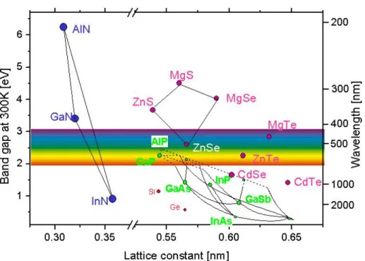
Figure 1.1 The bandgap diagram of compound semiconductor materials...7
Chapter 2
Figure 2.1 The diagram of GaN nano-pillars growth mechanism for (a) the nucleation process and (b) the growth process. The distance dCR represents the average (critical) distance from where Ga ad-atoms can reach the nano-pillar base that depends strongly on the growth temperature………18 Figure 2.2 SEM images of (a) GaN nano-pillar and (b) GaN film grown by MBE…19 Figure 2.3 The schematic illustrations of the growth procedure of GaN nano-pillar template………..20
Figure 2.4 SEM image of GaN NP template. The inset shows the funnel-like GaN NP……….21
Figure 2.5 The schematic diagram of GaN-based LED structure grown on GaN NP template………...22
Chapter 3
Figure 3.1 The setup detail of temperature dependent PL system………31
Chapter 4
Figure 4.1 (a) Cross-sectional SEM image of GaN NPs template; (b), (c) and (d) the procedure of the air-voids formation between a GaN NPs and u-GaN epitaxial layer……….…50 Figure 4.2 Surface morphology of overgrown GaN NPs template scanned by AFM..51
sapphire………...52 Figure 4.4 TEM image of (a) C-LEDs, (b) NP-LEDs, (c) HRTEM image of region I in (b) The diffraction condition is g=0002……….…53 Figure 4.5 (a) Cross-sectional SEM image, (b) the corresponding CL image of bulk GaN grown on NP template, and (c) CL spectra of bulk GaN grown on NP template in position 1, 2, 3 and 4………...54 Figure 4.6 The power-dependent PL efficiency curves of NP-LED and C-LED at 15 and 300 K………...56 Figure 4.7 The curves of integrated PL intensity versus the injected carrier density of (a) C-LED and (b) NP-LED………57 Figure 4.8 The emission peak energy and the FWHM of spectra as a function of the injected carrier density at 300 K for (a) C-LED and (b) NP-LED………58 Figure 4.9 Normalized integrated PL intensity as a function of 1000/T for (a) C-LED and (b) NP-LED. The activation energy is obtained from the Arrhenius plot………59 Figure 4.10 Schematic of effective localized states, defect states and activation
energy……….………60 Figure 4.11 Voltage and light output intensity versus forward current characteristics for C-LED and NP-LED………61 Figure 4.12 (a) 2D-FDTD of the calculated electric-field distribution of C-LED and NP LED; (b) enhancement factor of light output power versus the space of between air voids for C-LEDs and NP-LEDs………62
Chapter 1 Introduction
1.1 Characteristic of III-nitrides Materials
Nowadays, the III-nitrides materials have been widely used in semiconductor devices, for both optoelectronics and electronics. The III-nitrides materials, including AlN, GaN and InN with related alloys, cover a very wide range of direct bandgaps between 0.9 and 6.1 eV. Such wide range of direct bandgaps represents the emission wavelength from deep ultraviolet (UV) to infrared (IR) region as shown in figure 1.1.
With such wide emission wavelength range, III-nitrides materials is promising for applying in the applications of optoelectronic devices such as flat panel display, competing storage technologies, automobiles, general lighting and biotechnology, and so on [1-4]. Besides, among this wide emission wavelength range, the development of the emitted short wavelength light in the blue and UV region have attracted most attention. Because if we succeed in developing short wavelength devices, we are able to fill up the visible light gap and make the full color display by semiconductor material becomes possible. On the other hand, the emitted short wavelength light in the blue and UV region is especially suitable to pump up the yellow light and comes out a white light output by mixing the original blue source and excited yellow light which realized the solid state lighting.
suitable for lighting source in short wavelength in visible region but also high-speed/high-power electron device [5]. For instance, it has high bond energy (~2.3 eV), high-saturation velocity (~2.7 x 104cm/s), high-breakdown field (~2 x 10⁶ V/cm), and strong excitonic effects (>50 meV) [6-7].
Although III-nitride semiconductors are suitable for applying in high efficiency lighting devices, they also have some inherent drawbacks to deteriorate the lighting efficiency like internal piezoelectric field and spontaneous polarization at heterointerface leading to the quantum confined Stark effect (QCSE) and causing charge separation between electrons and holes in quantum wells [8-9]. Even though, it is still worth to devote more effort to overcome such problems for its great potential in solid state lighting and some groups had indeed succeeded in solving parts of this problems. In next section, the development of nitride-based light-emitting diodes will be introduced.
1.2 Development of Nitride-based Light-emitting Diodes
The first III-nitrides materials blue light-emitting diode (LED) could be retrospect to 1972. J. I. Pankove et al. fabricated it with metal-i-n structure [10]. Since that, several researches related to III-nitride-based LEDs had been carried on. Nevertheless, some severe problems might lower the efficiency and hinder the development of
III-nitride-based LEDs. The most important issue is the lack of suitable substrate for GaN epitaxy. For instance, sapphire substrate with a 15% smaller lattice constant than GaN, and different thermal expansion coefficient, leads to a very high defect density and cracking of the layers when the structures are cooled down after growth. The problem was firstly solved by Amano and Akasaki by designing and growing a AlN buffer layer in 1986 [11]. Also, Nakamura grew AlGaN buffer layers on top of sapphire in 1991 [12] which make it possible to grow GaN on sapphire. In addition to the invention of buffer layer, Prof. S. Nakamura also solved the high growth temperature problems by his two-flow growth reactor which was beneficial to high quality GaN material on sapphire [13].
On the other hand, p-type doping of GaN-based LED is another issue. Every semiconductor lighting device needs p-n junctions. Nevertheless, due to the highly background n-type concentration which was resulting from the native defects (commonly thought to be nitrogen vacancies) and residual impurities (such as Si and oxygen) acted as an efficient donor, p-type GaN performed poorly conductivity. But changes occurred after Akasaki’s work. Akasaki (1988 at Nagoya University) found that samples after Low Energy Electron Beam Irradiation treatment (LEEBI) showed p-type conductivity [14-15]. Thus Akasaki demonstrated that in principle p-type doping of GaN compounds was possible. Nakamura was then found the solution to
the puzzle of p-type doping. He found that previous investigators had annealed the samples in Ammonia (NH3) atmosphere at high temperatures. Ammonia dissociates above 400℃, producing atomic hydrogen. Atomic hydrogen passivates acceptors, so that p-type characteristics are not observed. As a result, Nakamura solved this problem by annealing the samples with nitrogen gas, instead of Ammonia [16].
With these technique mentioned above, the blue GaN-based light emitting diode (LED) is now successfully commercialized. A typical blue GaN-based LED is mainly consists of substrate, n-type GaN, MQWs, and p-type GaN. The layer of n-type GaN contains an excess of electrons, whereas the p-type layer is a region from which electrons have been removed (i.e., in which “holes” have been formed). If a forward bias is applied, electrons and holes can recombine, releasing energy in the transition layer in the form of light. The energy of the photon corresponds to the voltage bias in the transition region (the “bandgap”). Sapphire and silicon carbide are often used as substrates, which allow for large-area heteroepitaxial growth.
1.3 Motivation
With the effort of these pioneers, as mentioned in section 1.2, some severe problems had been solved. As a result, it is possible to use light-emitting diodes for solid state lighting. However, some inherent drawbacks, like internal piezoelectric field and spontaneous polarization at heterointerface leading to the quantum confined
Stark effect (QCSE) and causing charge separation between electrons and holes in quantum wells, still deteriorate the lighting efficiency. Besides, the lack of a suitable, inexpensive substrate restrains the improvement of GaN-based devices. Even though many semiconductor companies produce and sell pure GaN substrates today, their prices are always sky-high and not very accessible to ordinary applications. Typically, GaN-based epitaxial layers were grown on sapphire substrate by heteroepitaxial technique, such as metal-organic chemical vapor deposition (MOCVD) [17, 18]. However, due to the large lattice mismatch and thermal expansion coefficient misfit between GaN and sapphire, the subsequent-grown GaN epitaxial layers contained high threading dislocation densities (TD densities) (around 108-1010 cm-2) [19]. To improve the crystalline quality of GaN-based epitaxial layers on sapphire substrate, various growth techniques have been proposed, such as epitaxial lateral overgrowth (ELO) [20, 21], cantilever epitaxy (CE) [22], defect selective passivation [23], microscale SiNx or SiOx patterned mask [24-26], anisotropically etched GaN-sapphire interface [27], plastic relaxation through buried AlGaN cracks [28], and patterned sapphire substrate (PSS) [29-31].
Even with these techniques, it is still difficult to reduce TD density to a level ~ 107 cm−2 unless certain complicated or expensive method such as double ELOG [32] or epitaxy on GaN substrate [33] is used. Recently, nanoscale epitaxial lateral overgrowth (NELOG) was found to be a promising method. During the NELOG process, coalescence overgrowth of nanostructures will not only lead to improve crystal quality [34], but also produce a scattering effect on the emitted photons, leading to higher light extraction efficiency [35]. The nanostructures were generally fabricated by top-down methods [36-38], such as etching process, in which the dry etching procedure normally generates defect states on the column surfaces, causing
the reduction of internal quantum efficiency (IQE).
In this study, we report a NELOG of high-quality GaN layer on bottom-up nanostructure (self-assembled GaN nano-pillars (NPs)) grown by MBE [39]. Electro-optical properties of LEDs fabricated by the completed expitaxial structures grown on such GaN NPs template will also be discussed.
Chapter 2 Sample Structure and Fabrication
In recent years, more and more research group and institute are interested in nano-fabrication technology and take it in the application of GaN-based semiconductors. The nano-fabrication technology can attract such considerable interest and be widely used in optoelectronic and electronic devices because device with nano-fabrication technology has large different optical and electrical properties with those in the bulk materials. It is also reported that nano-fabrication technology device had great potential for better quantum confinement and strain relaxation effect [40].
GaN nanorods technology is one of the famous nano-structure which has been produced by various fabrication methods. In 1997, Han et al. first proposed synthesizing GaN nanorods by using carbon nanotubes as templates [41]. The dimension of the synthesized GaN nanorods could be up to 25 m in length and ranging from 4 to 50 m in diameter. However, it is not a simple method for produce GaN nanorods. The growth of single-crystal GaN nanorods by hybrid vapor-phase epitaxy [42] has been developed by Kim et al. A mask-free simple process by inductively coupled plasma-reactive ion etching (ICP-RIE) dry etching to fabricate GaN nanorods was proposed by Yu et al. [43]. The growth of GaN nanorods by using ferrocene as the catalyst, so-called vapor–liquid–solid (VLS) mechanism, was also
demonstrated [44]. Fabrication of GaN nanorods by e-beam patterning and ICP etching was proposed by Chen et al. [45].
With the rapid development of the nano-structure fabrication techniques, these technology had also been used in GaN devices. Johnson et. al demonstrated a single GaN nanowire lasing phenomenon in [46]. It is the first demonstration of single GaN nanowire laser. Han et. al. performed the photoconduction studies on GaN nanowire transistors under UV and polarized UV illumination in 2004 [47]. Besides, Kim et. al. demonstrated a high brightness LEDs by fabricating high quality, dislocation-free InGaN/GaN nanorods [48]. In 2006, Son et. al. demonstrated a UV photodetector by using a single GaN nanorod with p-n junction [49]. With the following literatures, we could know that GaN nano-stucture have played an important role in optoelectronic and electronic devices, such as laser, LED and photodetector.
From the following introduction of GaN nano-structures development, we could found that the nano-structures can be fabricated by two kinds of methods, fabrication process and epi-growth methods. In present production, the former has the advantage in the mass production. Nevertheless, fabrication process usually contains complicated steps in fabrication. In addition, some of these steps, like etching, might damage the crystalline quality and produce more defect, dangling bond and surface state, which often induced negative result and decreased the efficiency of devices.
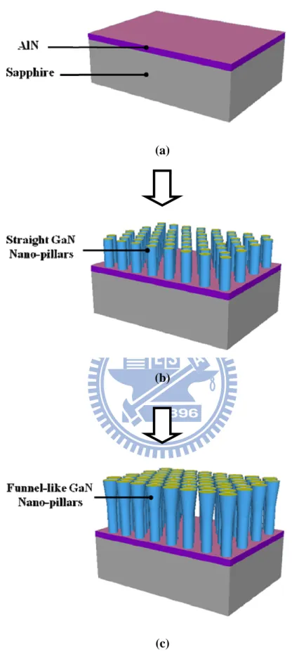
On the other hand, even though the epi-growth methods could not be used in mass production due to its low efficiency production, but it takes the advantage of better crystalline quality and can avoid complicated process. This chapter was divided into three parts. In chapter 2.1, we would introduce the growth model for growing GaN nano-pillar template by molecular beam epitaxy (MBE). Then we displayed how to grow funnel-like GaN nano-pillar template by MBE and re-grow LED structure on it by MOCVD in chapter 2.2 and 2.3, respectively.
2.1 Growth Mechanism of GaN Nano-pillar (NP) by MBE
In this section, we would introduce the growth mechanisms of spontaneous growth nano-pillars constructed by Jelena Ristic et. al [50]. would be cited to explain the growth procedure of GaN nano-pillar template.
As a matter of fact, the spontaneous growth of GaN nano-pillars had been achieved by a number of groups using molecular beam epitaxy (MBE) [51-55]. The characteristic of this kind of growth mechanism is that it does not require catalyst, but only adequate growth conditions, namely the III/V ratio and growth temperature. Moreover, it is noticeable that the nano-pillars diameter, density, and distribution could be controlled by different growth conditions.
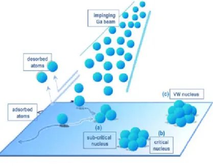
could be generalized to two different by connected aspects: (i) the nucleation process; and (ii) the growth process. The former determined the average nano-pillar size and density, while the latter gave rise to nano-pillars with constant diameter. Figure 2.1 (a) and (b) were the corresponding schematic drawings for the nucleation process and the growth process.
In the nucleation process, due to the naturally lattice mismatch between GaN and sapphire, the GaN growth mode would change from two dimensional (2D) to three dimensional (3D) under extreme nitrogen rich (N-rich) conditions. This phenomenon was driven by energy minimization to reduce the strain build-up between GaN and sapphire. The nucleation of thin films on a surface, from a vapor phase, generally started by atomic condensation as 3D nuclei that eventually formed a continuous film by a diffusion controlled process. According to the capillarity theory developed by Volmer and Weber, there is a critical size for these nuclei to become stable in terms of total free energy (volume and surface) [56]. If it below this value, nuclei might decay either by desorption or diffusion to other nuclei. On the other hand, the nuclei would aggregate of sizes larger than the critical one become stable deposits that kept growing by incorporation of diffusing atoms. If these critical nuclei are considered as spherical clusters, the critical radius (r) increases with the substrate temperature.
stable nuclei equals twice the Ga ad-atoms mean diffusion length that depends both on the growth temperature and the III/V ratio. For a given growth temperature, a decrease of the III/V ratio leads to a reduction of the Ga diffusion length [57] that determined the nano-pillar density and average diameter. When GaN was growing under extreme N-rich conditions (very small III/V ratio), stable nuclei would not coalesce because the arriving Ga ad-atoms will preferentially incorporate on their top. This preference was actually manifested by the tendency of hexagonal III-nitrides to generally grow in a pillar fashion (pillar grains). On the contrary, if Ga flux is increased (or N flux decreased) the saturation of the vertical growth will allow the onset of the lateral one, increasing the nucleation site diameter until coalescence, leading to a 2D layer morphology.
The fact that some time is required to reach the nano-pillars density saturation [58] can be understood in terms of a rather small Ga diffusivity (longer time to form stable nuclei), the small Ga arriving rate (very low Ga flux to keep nitrogen excess conditions) and the decreasing probability, as the nuclei density increases to stabilize a new nucleus out of reach from other stable nuclei already existing (see diagram in figure 2.1 (a)).
In summary, the nucleation of GaN nano-pillars can be seen as a process in which a certain number of Ga and N atoms get together by diffusion reaching the critical size.
This size may become larger, either at higher growth temperatures because of the increased Ga ad-atoms surface diffusion or by a substantial increase of the Ga flux (towards stoichiometry). In both cases, if the amount of active nitrogen is not high enough, a compact layer is obtained by islands coalescence. However, under extreme N-rich conditions, islands coalescence is blocked because of the preferential incorporation of metal atoms on the island top side, leading to a localized (nano-pillar) growth on the nucleated islands. As mentioned before, an increase of the growth temperature under these conditions leads to wider nano-pillars if the Ga flux is kept high enough to balance the enhanced Ga desorption [59]. Thus, the N-excess seems to impose an energy barrier to the kinetic processes related to Ga ad-atom surface diffusion in a similar way as it was predicted for N-rich growth on GaN surfaces [57].
During the nucleation process, the substrate surface becomes covered by GaN islands with different sizes (all are equal to or above the critical value) that yield differences in nano-pillar diameter. In addition, since the nucleation process does not occur simultaneously all over the substrate, some nano-pillars will start growing earlier than others giving way to the experimentally observed dispersion in heights. Moreover, variations in height among nano-pillars are expected due to the growth mechanism in which the Ga diffusion process along the nano-pillar sidewalls up to its apex can be a major contribution, thus, the wider the nano-pillar, the smaller its
growth rate [60].
Once a GaN island reaches its critical size and becomes stable, the nano-pillar started to grow on it following a process that depends on two contributions, namely: (i) Ga atoms impinging on the nano-pillar apex would incorporate directly to the crystal; and (ii) Ga atoms arriving to the substrate surface would diffuse to the nano-pillars base, climbed along the lateral sidewalls up to their apex and incorporated to the crystal [60,61], as shown by the diagram in figure 2.1 (b).
2.2 GaN Nano-pillar Template Grown by MBE
We had introduced the growth mechanism of GaN nano-pillar grown by MBE. Subsequently, we would show how to use the two-step method to grow funnel-like nano-pillars. Finally, we would discuss the advantage of this special template for the following re-growth.
In this research, the self-assembled GaN nano-pillar structure was grown on sapphire substrate by RF-plasma MBE (ULVAC MBE) system, and the related processes have been reported in our previous study [62].
From section 2.1, one could understand that the growth conditions (the III/V ratio and growth temperature) deeply influenced the appearance of GaN grown on sapphire. Before grew funnel-like GaN nano-pillar template, we had tested some conditions for
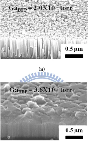
GaN (both nano-pillar and film) grown on sapphire. First, straight and uniform GaN nano-pillars was grown under the growth temperature, nitrogen flow rate, gallium flow rate and plasma power were Tg = 850℃, φN = 5.5 sccm, φGa = 2.0×10⁻⁷ torr and P = 500 W, respectively. As we increased the gallium flow rate (φGa = 3.6×10⁻⁷), namely increased the III-V ratio, the GaN film was formed. The SEM images of GaN nono-pillars and film were showed in figure 2.2 (a) and (b), respectively. This result was identical to the tendency of the growth mechanism (section 2.1), which elaborated that as the III-V ration increasing, the GaN nano-pillar diameter would also increase. If further increased III-V ration, GaN film would be formed due to the coalescence of GaN nano-pillar.
The above conditions were used to grow funnel-like GaN nano-pillar template and the growth procedure was showed in figure 2.3 (a), (b), and (c). The growth temperature, nitrogen flow rate and plasma power were also Tg = 850℃, φN = 5.5 sccm and P = 500 W, respectively. For better crystalline quality of GaN nano-pillar, AlN was directly grown on c-plane sapphire as a buffer layer. Then the two-step method was used by combining the two conditions (φGa = 2.0×10⁻⁷ and 3.6×10⁻⁷ torr) mentioned in preceding paragraph. First, the straight and uniform GaN nano-pillars were grown under N-rich condition (φGa = 2.0×10⁻⁷ torr) for one hour. Subsequently, funnel-like GaN nano-pillar were formed on straight nano-pillars under Ga flux
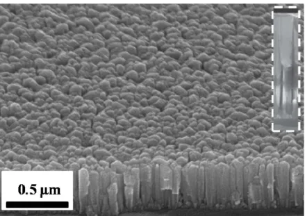
condition (φGa = 3.6×10⁻⁷ torr) for one hour. Figure 2.4 showed the SEM image of funnel-like GaN nano-pillars. It can clearly be seen that the GaN NP is funnel-like form shown on the inset of figure 2.4. It was reasonable that funnel-like GaN nano-pillars were formed, because of the increase of lateral growth rate and coalescence of GaN as III-V ratio increasing. In addition, the density, diameter and the height are estimated to be around 1.15×1010 cm−2, 50 nm and 0.8 µm, respectively.
In fact, the use of nano-pillar structures as a template for LED development had caught much attention recently because of the following advantages. First, the nanostructures can produce a scattering effect on the emitted light, leading to higher light extraction efficiency [63]-[66]. Second, the higher crystal quality can result in higher internal quantum wells (QWs) [67], [68]. Third, because of lateral strain relaxation, indium incorporation in growing InGaN/GaN quantum wells on an nano-pillar can be higher for longer wavelength emission [67].
In addition, funnel-like nano-pillar template with larger topmost surface, could further increase the lateral growth rate and promote better crystalline quality, which might be benefit for the LED device.
2.3 LED Structure Grown on GaN Nano-pillar Template by MOCVD
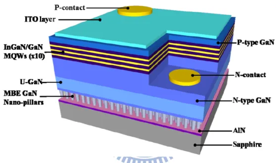
Next, we deposited a GaN-based LED structure on the NP/GaN template by a low pressure MOCVD (Veeco D75) system, denoted as NP-LEDs. In addition, the same GaN-based LED structure was also grown on sapphire without GaN NP for comparison, denoted as conventional LEDs (i.e., C-LEDs). During the growth, trimethylgallium (TMGa), trimethylindium (TMIn) and ammonia (NH3) were used as gallium, indium, and nitrogen sources, respectively. Silane (SiH4) and biscyclopentadienyl magnesium (CP2Mg) were used as the n-dopant and p-dopant source. The epitaxial structure of the GaN-based LED overgrowth on NP is depicted in figure 2.5, consisting of 30-nm GaN nucleation layer (GaN NL), 1-μm un-doped GaN (u-GaN), 3-μm n-doped GaN (n-GaN), 10-pairs InGaN/GaN multi-quantum wells (MQWs), and 0.2-μm p-doped GaN (p-GaN) cap layer.
In chapter 4, we would further discussed and compared the residual strain, crystalline quality, light extraction efficiency, optical and electrical characteristics between nano-pillar LED (NP-LED) and conventional LED (C-LED).
(a)
(b)
Figure 2.1 The diagram of GaN nano-pillars growth mechanism for (a) the nucleation process and (b) the growth process. The distance dCR represents the average (critical) distance from where Ga ad-atoms can reach the nano-pillar base that depends strongly on the growth temperature.
(a)
(b)
Figure 2.2 SEM images of (a) GaN nano-pillar and (b) GaN film grown by MBE with different Ga flow rate.
(a)
(b)
(c)
Figure 2.3 The schematic illustrations of the growth procedure of GaN nano-pillar template.
Figure 2.4 SEM image of GaN NP template. The inset shows the funnel-like GaN NP.
Figure 2.5 The schematic diagram of GaN-based LED structure grown on GaN NP template.
Chapter 3 Properties of III-nitride LED and Experimental Setup
In this chapter, we show the definition of internal quantum efficiency (IQE), light extraction efficiency (LEE), and external quantum efficiency (EQE). Subsequently, the IQE measurement method and experimental setup will be introduced.
3.1 Internal quantum efficiency (IQE)
The active region of ideal LED emits one photon when one electron injected. Each charge quantum-particle (electron) produces one light quantum-particle (photon). Thus the ideal active region of an LED has a quantum efficiency of unity. The internal quantum efficiency is defined as:
e / I h / P ond sec per LED o int injected electrons of number ond sec per region active from emitted photons of number int nt i
where Pint is the optical power emitted from the active region and I is the injection current. Photons emitted by the active region should escape from the LED die. In an ideal LED, all photons emitted by the active region are also emitted into free space. Such an LED has unity extraction efficiency. However, in a real LED, not all the power emitted from the active region is emitted into free space. Some photons may never emit into the free space. This is due to several possible loss mechanisms. For example, light may be reabsorbed by material itself of the LED. Light may be incident
on a metallic contact surface and be absorbed by the metal. In addition, the phenomenon of the total internal reflection, also referred to as the trapped light phenomenon, reduces the ability of light to escape from the active region.
Another view point, the internal quantum efficiency in a semiconductor is related to non-radiative recombination centers. If the radiative lifetime is denoted as τr and the non-radiative lifetime is denoted as τnr, then the total probability of recombination is given by the sum of the radiative and non-radiative probability:
nr r
1
1
1
(3-1)The relative probability of radiative recombination is given by the radiative probability over the total probability of recombination. Thus the probability of radiative recombination or IQE is given by:
1 nr 1 r 1 r int
(3-2)The IQE gives the ratio of the number of light quanta emitted inside the semiconductor to the number of charge quanta undergoing recombination. Note that not all photons emitted internally may escape from the semiconductor due to critical
By the above equation, the internal quantum efficiency is determined by the competition between radiative and nonradiative recombination processes. In this material system, the radiative recombination rate is affected by the quantum-confined Stark effect (QCSE) and exciton localization effects. Although the relative importance of these contributions has been widely studied in recent years, many questions regarding the emission process still remain.
3.2 Light extraction efficiency (LEE) and external quantum efficiency (EQE)
The extraction efficiency can be a severe limitation for high performance LEDs. It is quite difficult to increase the extraction efficiency beyond 50% without resorting to high sophisticated and costly device processes. The light extraction efficiency (LEE) is defined as: h / P h / P ond sec per region active from emitted photons of number ond sec per space free o int emitted photons of number int extraction (3-3)
where P is the optical power emitted into free space. Considering the refractive indices of GaN (n = 2.5) and air, for the light escape cone is about 23% due to the critical angle. Assuming that light emitted from sidewalls and backside is neglected, one expects that approximately only 4% of the internal light can be extracted from a
surface. The light outside the escape cone is reflected into the substrate and is repeatedly reflected, then reabsorbed by active layers or electrodes, unless it escapes through the sidewalls. However, there is much room for improvement of the light extraction efficiency. For example, roughening of the top LED surface increased the light extraction efficiency.
Finally, the external quantum efficiency (EQE) is defined as:
(3-4) from the above equation, we can know that the EQE depend on IQE and LEE, therefore, the improvement of IQE and LEE pay an important role of LED. Recently, the patterned sapphire substrate is introduced to improve the IQE which is attributed to reduce the dislocation density and enhance the LEE due light emit to substrate may reflect and emit into free space.
3.3 IQE Measurement Method
Generally, we used temperature dependent PL measurement and investigate the PL intensity variation curves with temperature to define IQE. It is a non-destructive method to understand the internal material characteristics and quality. It provides useful information about emission wavelength, light intensity and other optical
extraction ext I e h P ond per LED o injected electron of number ond per space free o emitted photons of number / int / sec int sec int
properties. During the experiment period, the intensity gradually reduced with the rising temperature. We could reasonably assume there are no non-radiative recombination at 0 K and the IQE approaches 1 which means one photon generated in the MQW while one laser photon was injected into the MQWs. In the meantime, we assume the ExE would not change with the increasing temperature. Therefore, the IQE could be defined as equation 3-5 by the traditional method:
) 0 ( ) ( ) ( int I T I T (3-5)
where I(0) stands for the PL intensity at 0K and I(T) implies the PL intensity under specific temperature. We note that this method ignores the influence of injected laser power density which is not valid in blue GaN-based LED material system. Hence, we quote reference [69] to give a new definition by PL method. We performed the power-dependent PL measurement at low temperature and room temperature and define it by observing the tendency of the curves. This could be expressed as the following equation 3-6: int / / inj inj PL PL PL E I E I C (3-6)
where IPL is the collected PL intensity; Iinj is the injected laser intensity; EPL is the
measured light photon energy; Einj is injected photon energy and C is a constant which
is related to carrier injection efficiency, light extraction efficiency and correction efficiency of PL.
As the injected laser power increased, the collected light intensity also increased. Generally, we could collect higher PL intensity at low temperature than that in room temperature. We then can calculate the collected photons to be divided by the injected laser photons, by equation 3-6. A maximum number would be observed at some power of low temperature curve. After normalization to the peak of low temperature curve, we could define the IQE at room temperature at different laser power.
3.4 PL Measurement Setup and Experiment
For excitation power and temperature dependent PL measurement, the laser source used in this research is femto-second-pulse Ti:sapphire. The output laser wavelength could be tuned to be around 760-820 nm by adjusting the internal resonant length and gain profile. A frequency doubler and tripler crystal is setup at the laser output optical path. Here, we adopted the doubler crystal to have a wavelength at around 380-410 nm could be obtained. It is specifically important in avoiding the absorption of GaN material itself and ensured most of the injected laser photons could excited the
photons inside the MQWs. We note that this assumption essential while we predicted the injected carrier density. The tuned the 380-410 nm laser was then incident into the sample surface vertically. The sample was mounted in a closed-cycle He cryostate with a temperature controller which could be precisely controlled in the temperature region around 15 to 300 K. By the temperature controller with a set of wire heater, we could perform a serious of temperature-dependent experiments from 15 to 300 K. The luminescence signal dispersed through a 0.55-meter monochromator was detected by the photomultiplier tube (PMT). The setup detail of temperature dependent PL is shown in figure 3.1.
After the facility setup, we are then starting the optical experiments. A filter and a power meter were placed before sample chamber to modify and control the laser output power. By rotating the filter, we could vary the excitation power changing from 5x10⁻³ mW to 80 mW. We note in every PL measurement setup, the diameter of laser spot might have different spot size. Therefore, though we could plot the relationship between the injected power and the efficiency, it will be more convenient for comparison and reflect the influence of the carrier density more clearly, if we could transfer the power intro carrier density. To do that, we could follow the equation below to transfer our injected power to carrier density:
Injected Carrier Density *exp( )*[1 exp( )]*(1 ) * * * ) (h d f d d R P active InGaN GaN GaN active (3-7)
The injected carrier density is determined primarily by the power of pumping laser (P), the energy of injected photon (hv), the spot size of pumping laser (φ), the thickness of GaN and active region (dGaN ,dactive), the repetition rate of pumping laser
(f), the absorption efficiency of GaN and InGaN (αGaN, αInGaN), and the reflectance of
pumping laser (R), as expressed by the following equation. Experimentally, we choose φ = 50 μm, dGaN = 200 nm, dactive =156nm, αInGaN =105 cm-1, repetition rate of
the laser = 76 MHz and R=0.17 to calculate the injected carrier density in our samples. Here we ignore the absorption of GaN since the energy of pumping photons is less than its energy bandgap,i.e. αGaN =0.
Chapter 4 Results and Discussion
4.1 Characteristic of bulk GaN grown on GaN nano-pillar template
The results of the bulk GaN grown on GaN nano-pillar template like SEM images, AFM images and Raman spectrum will be discussed in this section.
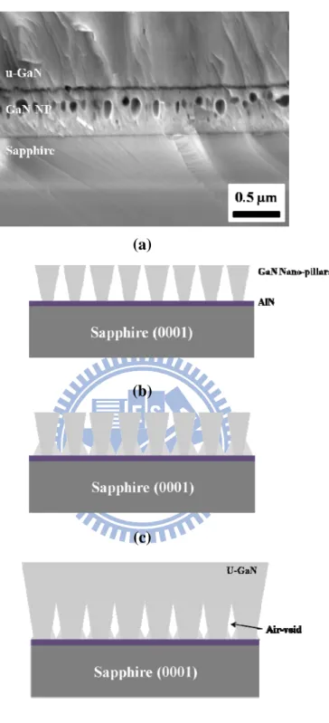
Figure 4.1 (a) shows the cross-sectional SEM image of bulk GaN grown on GaN nano-pillar template. As shown in figure 4.1 (a), there is a row of air-voids formed between GaN nano-pillars. Figure 4.1 (b), (c) and (d) shows what happened to these nano-pillars after re-growth and discussed the procedures of the air-voids formation between GaN nano-pillars and u-GaN epitaxial layer. First, funnel-like shaped GaN nano-pillars were formed on a sapphire substrate by MBE shown in figure 4.1 (b). As the nano-pillar grows upwards, there is also lateral growth happening between the pillars. Such lateral growth eventually narrows the gap between columns and forms holes with 0.2 to 0.25 µm in size, which is shown in figure 4.1 (c). Meanwhile, the GaN nano-pillars growth temperature is about 850oC in MBE. Next, we transfer the template to MOCVD system to finish the growth. The re-growth temperature of GaN film is about 1050oC. Under this high temperature, re-crystallization of GaN is very possible and final coalescence u-GaN NPs template was performed and air-voids were formed as show in figure 4.1 (d). As we can see, the air-voids shown in figure 4.1 (a) are with diameter of 100nm, and shall be able to increase the light extraction
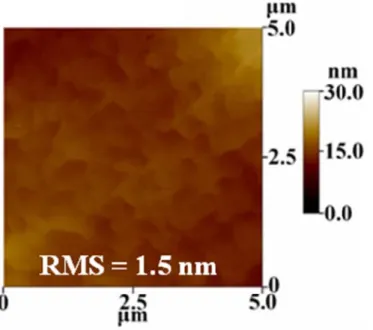
efficiency (LEE) due to extra light scattering from these embedded air bubbles [70]. After the u-GaN layer was deposited, the surface morphology was measured by atomic force microscopy (AFM), as shown in figure 4.2. The root mean square (RMS) value of the surface roughness is about 1.5 nm. Although it was not flat as general bulk GaN grown on sapphire, it is flat enough for the following LED structure re-growth. This indicated that the effect of u-GaN coalescence overgrown on GaN nano-pillar template was happened.
To analyze the residual strain in the GaN films, Raman backscattering measurements were performed at room temperature. Figure 4.3 shows the Raman spectrum for GaN epitaxial layer grown on sapphire with and without GaN NPs. The Raman shift peaks of E2 (high) mode for GaN epitaxial layer grown on sapphire with and without GaN NPs are located at around 567.4 and 569.3 cm-1, respectively. Accordingly, the in-plane compressive stress σ for GaN epitaxial layer is estimated to decrease from 1.33 GPa to 0.44 GPa with presence of GaN nano-pillar templates, by using the following equation [71] :
(4-1)
where Δω is the Raman shift peak difference between the strained GaN epitaxial layer
E
E
C
ωE2 and the unstrained GaN epitaxial layer ω0 (566.5 cm-1); C is the biaxial strain
coefficient, which is 2.25 cm-1/GPa. Consequently, we can expect that the GaN-based LED grown on such strain relaxation template have weaker quantum-confined Stark effect (QCSE) [72].
We had demonstrated the characteristic of bulk GaN grown on GaN nano-pillar template and this can be attributed to the following factors: first, a row of air voids formed between GaN nano-pillars due to the coalescence overgrowth of GaN. Second, the surface morphology of bulk GaN is flat enough for the following LED structure re-growth. Third, the residual strain of bulk GaN grown on GaN nano-pillar was almost free due to the strain relaxation of GaN nono-pillar template.
4.2 Crystal quality analysis of the overgrowth GaN on nano-pillar template
The TEM was employed to investigate the crystalline quality of GaN epitaxial layer grown on a planar sapphire substrate and on a nano-pillar template. As we can see from figure 4.4 (a), in the case of the GaN epitaxial layer grown on sapphire without GaN NPs, numbers of threading dislocation propagate vertically from the interface between GaN and sapphire, all the way to the top device layers. As a result, the TDs density in conventional GaN layer is higher than 109 cm-2. Whereas, for the GaN epitaxial layer grown on sapphire with GaN NP (figure 4.4 (b)), it can be clearly
found that the crystallography is drastically different from that of conventional ones. Fewer TDs are observable within the range in view. The dislocation density on the top of n-GaN, MQWs is calculated to be around 7×107 cm-2. The reduction of TDs density can be attributed to the misfit (mainly perpendicular to the c-axis) and dislocation bending occurred just above the voids, as shown in the inset of figure 4.4 (c). Such behaviors are similar to those occurred in the nanoscale epitaxial lateral overgrowth (NELOG) method on a SiO2 nanorod-array patterned sapphire substrate [73].
Moreover, to confirm that using nano-pillar template and the LED structure overgrown on it could improve crystalline quality exactly, the cross-sectional cathodoluminescence (CL) was employed. Figure 4.5 (a) and (b) show a cross-sectional SEM image and the corresponding CL image of the overgrown sample. In the initial stage of MOCVD overgrowth, nano-pillars may merge quickly because of the small spacing of the funnel-like nano-pillar. This caused final coalescence of u-GaN and air-voids were formed in GaN nano-pillar layer. As we could see in figure 4.5 (b), the CL image shows a strong contrast between the bright emission in the relatively upper part of the overgrowth u-GaN layer and the dark background in the nano-pillar layer and the relatively lower part of the overgrowth u-GaN layer. It is clear that the relatively upper part of the overgrowth u-GaN had better quality with the stronger emission than the other part. On the other hand, the nano-pillar layer and
the relatively lower part of the overgrowth u-GaN had worse quality with dark emission. We discussed this individually and deliberated two possible causes. First, the optical quality of the higer-temperature GaN overgrowth layer is better than that of the lower-temperature grown GaN nano-pillar. Normally, a lower-temperature grown GaN has a higher point defect density, leading to lower internal quantum efficiency. This might be the possible reason for why the CL emission in the region of GaN nano-pillar was not bright as the upper u-GaN. Second, during the overgrowth stage, low-quality GaN might have filled in the space between nano-pillars and produce defects and dislocations. These defects and dislocations were regarded as nonradiative centers and dominated the CL behavior.
Above the low-quality u-GaN layer, the crystalline quality was improved gradually through nanoscale epitaxial lateral overgrowth (NELOG) as mentioned above. The high-quality u-GaN with low threading dislocation density (TDDs) was shown in figure 4.4. To prove what we had inferred about the growth mechanism of NELOG, the cross-sectional CL spectrum with different thickness of GaN was also employed. We chose four different thickness apart from the topmost nano-pillar layer by 1μm, 2μm, 3μm and 4μm, respectively. As shown in figure 4.5 (c), we could find that each CL spectrum had two peaks at 370 nm and about 556 nm, representing GaN emission peak and yellow band peak. The yellow band was often considered as
emission from defects and dislocation. As a result, we tried to use the ratio of GaN peak height and yellow band peak height to quantify the crystalline quality. The peak height ratio of GaN and yellow band of 1μm, 2μm, 3μm and 4μm from the topmost of nano-pillar layer were 3.24, 11.36, 21.74 and 19.23, respectively. From 1μm to 3μm, the trend of the peak height ratio of GaN and yellow band was gradually increasing, indicating the improvement of crystalline quality. From 3μm to 4μm, it was decreased from 21.74 to 19.23. Nevertheless, this amount of difference is not large enough to influence the crystalline quality remarkably and this result might be localized effect. So we didn’t discuss about it further.
In this section, we had demonstrated the procedure of coalescence overgrowth GaN on nano-pillar template. The TEM image indicated that the threading dislocation densities was decreased to 7×10⁷. Also, by CL mapping and spectra from different thickness, brighter emission and higher peak height ratio of GaN and yellow band for upper GaN could be the evidence for our inference of the growth procedure.
4.3 Optical characteristic of NP-LEDs
In order to confirm the efficiency improvement of our NP-LED, the PL internal quantum efficiency (IQE) measurement was performed. A general approach to evaluate the IQE of LEDs is to compare the PL integrated intensity between low and
room temperatures [74]. Figure 4.6 shows the measured quantum efficiency as a function of excitation power at 15 K and 300 K for NP-LEDs and C-LEDs. The efficiency is defined as the collected photon number divided by the injected photon numbers and normalized to the maximum efficiency of low temperature [75].
For the LED grown on planar sapphire substrate and GaN nano-pillar template, one could clearly see that the IQE increased with injected carrier density increased to reach its maximum and decreased as the injected carrier density further increased. The tendency of this two efficiency curves at 15 K and 300 K was quite similar. But under low injection carrier density range, the IQE at 300 K increased more pronounced than it at 15 K. The corresponding density to the peak efficiency for the LED grown on planar sapphire (44.3%) in 300 K is at injected carrier density of about 4×1017 cm-3, which is larger than it at 15 K, about 4×1016 cm-3. On the other hand, for the LED grown on GaN nano-pillar template, a similar dependence of the IQE on the injected carrier density was observed. Nevertheless, in term of the peak efficiency (55.9%) in 300 K at injected carrier density of 2×1017 cm-3, the IQE of LED grown on the NP template was enhanced by ~26.2%. It means that under the same injected power of pumping laser, there is about 26.2% enhancement for the converted photon carriers within the active region, as compared to the conventional LED structure grown on planar sapphire substrate. Moreover, at the corresponding generated carrier density of
8×1017 cm-3 (20mW) it can be found that the IQE increase from 41.9% for C-LEDs to 53.1% for NP-LEDs, At this excitation level, we could calculate the corresponding generated carrier density, approximately same level of 20 mA at room temperature in our device. Thus, the better emission efficiency of GaN- NP based LED can be linked directly due to the improvement of IQE and much better crystal quality, attributed to NELOG on nano-pillar template and reduction of threading dislocations, as mentioned in previous section. Besides, we would further discuss about the mechanism responsible for the dependence of IQE on the injected carrier density for LEDs grown on planar sapphire and nano-pillar template.
It was been reported that the collected PL intensity, L, is proportional to the injected carrier density, I, with a power index P. This could be expressed as [76, 77]
L α IP (4-2)
where parameter P physically reflects the various recombination process. If P equals to 1, it indicates the radiative recombination dominates. On the other hand, P>1, the Shockley-Read-Hall (SRH) recombination occurs, which was related to the presence of nonradiative centers and might be a shunt path to the current. Figure 4.7 (a) and (b) were the relationship between injected carrier density and the PL intensity of both
LED samples grown on planar sapphire and nano-pillar template.
At 15 K for LED sample grown on planar sapphire and nano-pillar template, the PL intensity is almost linearly varied with excitation power density and the power index was equal to 1, indicating that the radiative recombination dominated the recombination process at all injected carrier density range. It was reasonable that the radiative recombination dominated all the recombination process at 15 K, since the nonradiative centers would be quenched generally at such low temperature closed to absolute zero. Nevertheless, under low excitation injected carrier density at 300 K, the superlinear dependence of L on I are observed for both LED samples grown on planar sapphire and nano-pillar template. This means that defect related nonradiative recombination dominates the recombination process in this low carrier injection range at room temperature. But as injected carriers continuously increased, the linear dependence of the PL intensity to the injected carrier density is exhibited. It was noteworthy for both LED samples in 300 K, the value of P decreased from P>1 to P=1 gradually with the increasing of injected carrier density, instead of jump to 1. It means the nonradiative centers are saturated and leads to the gradual suppression of the nonradiative recombination with the injected carrier density. Therefore, the radiative recombination started to dominate the recombination process, resulting in the pronounced increasing of the IQE, as shown in figure 4.6, for the region of injected
carrier density less than 4×1016 cm-3.
From the preceding discussion, we concluded that the value of P in the superlinear zone could reflect the different crystalline quality and amout of nonradiative centers (such as defect and threading dislocations) between the two LED samples grown on planar sapphire and nano-pillar template. The value of P for LED samples grown on planar sapphire and nano-pillar template were 1.55 and 1.21, respectively, indicating that LED grown on sapphire had more nonradiative recombination centers than LED grown on nano-pillar template. This result was similar to the crystalline quality analysis in section 4.2.
In addition to the optical characteristic mentioned above, we could get more information from the PL spectrum and further investigated the optical mechanisms which affected the IQE result. We tried to analyze the emission peak energy and the FWHM of spectra as a function of the injected carrier density at 300 K for this two LED samples, LED grown on planar sapphire and nano-pillar template. For the LED grown on planar sapphire substrate, several unique optical properties were observed at 300K, as shown in figure 4.8 (a). First, the emission peak energy gradually decreased with the injected carrier density ranging from 8×1014 cm-3 to 4×1016 cm-3, and an opposite trend was observed as the injection carriers further increased. Second, the FWHM of spectra shrinks when the injection carrier density ranging from 8×1014 cm-3
to 4×1016 cm-3, and an opposite trend was observe as the injection carriers further increased.
In the region of the injected carrier density from 8×1014 cm-3 to 4×1016 cm-3 in figure 4.8 (a), the emission energy showed the red-shift and the FWHM shrank with increasing injected carrier density. As can be seen in figure 4.7 (a) in this section, the parameter P in this region is larger than 1, indicating the nonradiative recombination dominated the carrier recombination process. Under this circumstance, the excited carriers tended to recombine at higher energy extended states before reaching into lower energy localized states [78]. However, with the increasing of the injected carrier density, the nonradiative recombination was gradually bleached out and the carriers could reach into lower energy localized states easier. This is why the emission energy showed the red-shift and the FWHM shrank with increasing injected carrier density.
On the other hand, as the injected carrier density further increasing, other mechanisms dominated the optical characteristic. In general, there are two mechanisms responsible for the blue-shift of emission energy with increasing injected carrier density. The first is the so-called coulomb screening of the quantum-confined Stark effect (QCSE). This effect occurred in the general InGaN/GaN MQWs because the internal field direction is parallel to the MQWs growth direction. As a result, the devices with the general InGaN/GaN MQWs often endure a strong QCSE. It caused a
band tilting and a separation of wavefunction between electrons and holes, which resulting in a wavelength redshift and recombination efficiency reduction. Nevertheless, the increasing of injected carrier density could weaken the QCSE, that is why we called this effect as the coulomb screening of the QCSE. Therefore, an increasing trend of transition energy and efficiency might be observed if this effect dominates. Moreover, as the screening effect dominates the emission process, it accompanied a reduction in FWHM, due to QCSE was restrained, resulting in the effect of band tilting had become quenched and further overlapping the wavefuction between electrons and holes.
The second is band filling effect of localized states, which is an effect for carriers filled at a higher energy level while the injected carrier density increased continuously. For the InGaN/GaN material, indium composition inhomogeneity and monolayer thickness fluctuation were occurred commonly in the InGaN MQWs. Such self-organized In-rich region was generated in InGaN active region, resulting in potential fluctuation of the energy bandgap [79-81]. As further increasing the injected carrier density, the filling effect of high energetic localized centers started interfering and become dominated, that also induced a blue-shift of emission energy. However, different from the effect of QCSE, this effect accompanied the broadening of FWHM.
injected carrier density at 300 K for the LED grown on GaN nano-pillar template. Compared with the LED grown on planar sapphire, it was apparent that the variation in both the emission energy and the FWHM were smaller. We concluded this phenomenon into three parts. First, at low injected carrier density (8×1014 cm-3 to 4× 1016 cm-3), the LED grown on nano-pillar with the smaller parameter P (1.21 and 1.55 for NP-LED and C-LED, respectively) had less threading dislocations and nonradiative centers. This result also decreased higher energy extended states and carriers could reach into lower energy localized states without the influence of nonradiative centers. This is why the variation of the emission energy red-shift and FWHM for NP-LED were smaller than C-LED. Second, for the region of the injected carrier density from 4×1016 cm-3 to 2×1017 cm-3, the radiative recombination become dominated (P=1), leading to coulomb screening of the QCSE. However, the Raman spectra of bulk GaN grown on nano-pillar template, as shown in figure 4.3 in section 4.1, demonstrated that the residual strain was almost free for bulk GaN grown on nano-pillar template. As a result, we could expect that the coulomb screening of the QCSE was moderate for NP-LED. This expectation was also confirmed by the peak energy and FWHM as a function of injected carrier density. Third, as the injected carrier density increasing continuously, as mentioned before, the band filling effect of localized states dominated. The reason for moderate variation in both peak energy and
FWHM for NP-LED might because more uniform for the indium composition inhomogeneity and monolayer thickness fluctuation. On the other hand, the C-LED with larger residual strain might bring about different size of indium clusters, resulting in inhomogeneity of indium composition and mono layer thickness.
All the information provided above could be the evidence to explain the origin of higher IQE for the LED grown on nano-pillar template. Besides, we tried to use another method to analyze about this. Here, we collected the temperature dependent PL intensity and plot the normalized intensity with inversed temperature which is understood as Arrhenius plot in figure 4.9. Then, this temperature dependent curve could be fitted by the following equation to get the activation energy:
IT = I0 / [1+A exp(-Ea / kT)+B exp(-Eb / kT)] (4-3)
Where IT, I0 are the integrated PL intensity for T and 0 K, A and B are constants, k is the Boltzmann constant, T is the temperature, Ea is the activation energy for PL quenching, and Eb is generally associated to the free exciton binding energy [82]. The fit activation energy for the LED grown on the planar sapphire and nano-pillar template are 79 meV and 62 meV, respectively. In general, the activation energy can be explained by the ability to confine the carriers within the potential minima. One
could understand it through the schematic of activation energy in figure 4.10. It had been understood that because of the indium inhomogeneous in InGaN material system, there are a large indium fluctuation and a various localized states. The average of this localization could be quantized as an effective localized state. On the other hand, because of a large density of dislocation which results in a nonradiative recombination, we could also summarize this state as a effective defect state. The difference between these two states could be regarded as the so-called activation energy. One could also realize it as one kind of energy to enable a confined electron trapped in the localized state escaping from it. As a result, we could conclude that higher value of the activation energy indicates the stronger confinement of injected carriers and that certainly promises the higher IQE.
We demonstrated the PL internal quantum efficiency (IQE) measurement and found out that NP-LED had larger IQE than C-LED. To analyze the variation of IQE for both NP-LED and C-LED, we further compared the difference of peak energy and FWHM as a function of infected carrier density and temperature dependent PL. All the evidences revealed that NP-LED with higher IQE had better performance in optical analysis.
4.4 GaN nano-pillar LED device performance
LED devices with a chip size of 350×350 m2 were then fabricated from the completed expitaxial structures grown on sapphire with and without GaN NPs mentioned above. Figure 11 displayed the typical power-current-voltage (L-I-V) characteristics of NP-LEDs and C-LEDs. With an injection current of 20 mA, the forward voltages are 3.38 and 3.40 V, the light output obtained from the NP-LED device was higher than C-LED by 71% at 20 mA. The nearly identical I-V curves indicated that the different template (with and without nano-pillar) had little impact on I-V characteristics. Moreover, the NELOG of GaN did not deteriorate the electrical properties. On the other hand, the light enhancement of I-V characteristics by 71% can be attributed to the following factors: first, the NP-assisted NELOG method effectively suppressed the TD density of epitaxial layers. This reduction leads to much lower non-radiative recombination events in the nano-pillar devices and increase the photon generation efficiency. Second, the radiative recombination rate is also improved by stronger wavefunction overlap due to the weaker QCSE after strain relaxation. Third, as mentioned before, we expected that more light could be extracted from the LED because of the light scattering from the embedded nano-scaled air voids. In conclusion, we had demonstrated the L-I-V characteristic of GaN nano-pillar LED device. Compared with C-LED device, NP-LED device had nearly identical I-V
characteristic with C-LED. Besides, it displayed higher light output than C-LED by 71%. Nevertheless, as one can know that the light output enhancement must be acquired by both the IQE enhancement and light extraction efficiency (LEE). For improving our hypothesis that the embedded nano-scaled air voids could induce more light extracted from LED by light scattering, we tried to construct a model which was similar to the air voids embedded in nano-pillar layer.
4.5 Light extraction efficiency simulation by FDTD
A 2-D finite difference time domain (FDTD) mathematical technique was applied to calculate the LEE of the LEDs using the FullWAVETM program [83].The simulated structure with calculated electric-field distribution under the condition of air void distance 0.25 μm. is shown in Fig. 12 (a), where an array of air-filled rectangular holes represents air voids in our devices. The size of each rectangular hole is 0.2 μm×0.1μm. We set single dipole illumination sources placed at 0.5 μm below the top of surface structures and the detector around the simulated device [84]. As can be seen, the electric-field intensity of NP-LEDs is higher than C-LEDs above the monitor. It indicates the photons emitted from the MQWs were less trapped in the GaN layer and more propagated vertically. The corresponding normalized light output as functions of the simulation time are calculated and plotted in figure 12 (b), where the
normalized light output is defined as the ratio of steady light output of NP-LEDs to that of C-LEDs. It can be seen that the light output of NP-LEDs reaches its steady-state is less than 200 fs while that of C-LEDs saturates within 50 fs. In addition, from the study of light output of NP-LEDs is around 1.48 times higher than that of the C-LEDs. Combined with previous PL IQE measurement, we can see a total enhancement of 83% (48% from LEE and 24% from IQE) compared to conventional LED structure. The actual increase in light output of LED, which is 71%, is lower than prediction. This is possibly due to randomness of the air-void formation, which makes our FDTD analysis overestimating the light scattering effect.
(a)
(b)
(c)
(d)
Figure 4.1 (a) Cross-sectional SEM image of GaN NPs template; (b), (c) and (d) the procedure of the air-voids formation between a GaN NPs and u-GaN epitaxial layer.
Figure 4.2 Surface morphology of overgrown GaN NPs template scanned by AFM.
Figure 4.3 Raman spectrum for GaN epilayer overgrown on GaN NPs template and sapphire.
Figure 4.4 TEM image of (a) C-LEDs, (b) NP-LEDs, (c) HRTEM image of region I in (b) The diffraction condition is g=0002.
Figure 4.5 (a) Cross-sectional SEM image and (b) the corresponding CL image of bulk GaN grown on NP template.
Figure 4.5 (c) CL spectra of bulk GaN grown on NP template in position 1, 2, 3 and 4.
Figure 4.6 The power-dependent PL efficiency curves of NP-LED and C-LED at 15 and 300 K.