國 立 交 通 大 學
電子工程學系 電子研究所
博 士 論 文
應用新穎微影及奈米微晶粒技術於奈米元件與
記憶體之研究
Application of novel lithography and
nano-crystal technique in the fabrication of
nano-devices and memories
研 究 生 :游 信 強
指導教授 :雷 添 福
柯 富 祥
應用新穎微影及奈米微晶粒技術於奈米元件與記憶
體之研究
Application of novel lithography and nano-crystal
technique in the fabrication of nano-devices and
memories
研究生:游信強 Student:Hsin-Chiang You
指導教授:雷添福 博士
Advisor:Dr. Tan-Fu Lei
柯富祥 博士
Dr. Fu-Hsiang Ko
國立交通大學
電子工程學系 電子研究所
A Dissertation
Submitted to Department of Electronics Engineering
and Institute of Electronics
College of Electrical and Computer Engineering
National Chiao Tung University
In Partial Fulfillment of the Requirements
For the Degree of
Doctor of Philosophy
in
Electronics Engineering
July 2006
Hsinchu, Taiwan, Republic of China
應用新穎微影及奈米微晶粒技術於奈米元件與
記憶體之研究
學生: 游 信 強
指導教授: 雷 添 福 博士
柯 富 祥 博士
國立交通大學
電子工程學系 電子研究所博士班
摘 要
首先我們研發出一種新的製程技術包括:電子束寫入、化學微縮以及二氧化 矽蝕刻用來製作低於 60 奈米的接觸孔洞。接著使用CHF3/CF4混合的氣體蝕刻二氧 化矽以形成奈米尺度大小的接觸孔洞。在蝕刻過程中,化學微縮阻劑在電漿蝕刻 時側壁會形成高分子聚合物使得奈米孔洞縮小。孔洞的周長面積比例反應出經過 蝕刻後孔洞尺寸的縮小情形,尤其對於小尺寸的接觸孔洞。蝕刻時在側壁形成的 高分子聚合物可有效的縮小奈米孔洞尺寸。 再者將碳六十和碳七十加入電子束阻劑,稱為電子束阻劑修飾法,藉由加 入少量的碳六十和碳七十,即可得到高解析度、小線寬以及高抗蝕刻能力之阻 劑。使用阻劑修飾法可定義出低於 50 奈米的接觸孔洞及線、亦可應用在定義自 我對準金屬矽化物的複晶矽以得到較低奈米線的片電阻值。本方法亦可增加阻劑 對二氧化矽及複晶矽的選擇蝕刻比。接著,我們使用鎳金屬自我對準矽化物和氨電漿處理來製作 50 奈米閘極長 度的奈米鰭型元件。我們發現元件特性使用深層鎳金屬自我對準矽化物製程與沒 有使用鎳金矽化物製程比較可以得到有效的改善,包括:次臨界擺動、汲極引發 位能障降低、提升元件電流導通關閉比,。深層鎳金屬自我對準矽化物元件可以 有效的抑制浮接基體效應和寄生 BJT 效應。 再來,我們發展一個非常簡單製備二氧化鋯薄膜的方法,包含:在冰浴中製 備ZrCl4前驅物、溶膠-凝膠法沉積、烘烤以及退火等步驟。我們可使用前驅物的 濃度控制薄膜厚度。關於薄膜的電性方面,如:有大的崩潰電場、低的閘極漏電 流密度顯示出經過了 900 度的快速熱退火後,具有絕佳的絕緣體特性。使用溶膠 -凝膠法製備的二氧化鋯薄膜可應用在電容的絕緣材料上。 最後我們使用簡單的溶膠法以及 900 度的快速熱退火來製備三種 SONOS 型 記憶體元件,其一為以二氧化鉿薄膜作為 SONOS 型記憶體元件的陷捕電荷層,其 二為以氧化鉿奈米微晶粒作為 SONOS 型記憶體元件的陷捕電荷層,其三為以氧化 鋯和氧化鉿奈米微晶粒共存作為 SONOS 型記憶體元件的陷捕電荷層。這是溶膠法 第一次使用在奈米微晶粒的記憶體元件製備上。SONOS 型記憶體元件以氧化鋯和 氧化鉿奈米微晶粒共存作為陷捕電荷層有較大的臨限電壓漂移和較快的寫入、清 除。此外這三種 SONOS 型記憶體元件電性方面都有不錯的特性表現,如: 長時間 的資料持久性,以及好的寫入、清除操作造成的性能退化少特性。
Application of novel lithography and
nano-crystal technique in the fabrication of
nano-devices and memories
Student: Hsin-Chiang You
Advisor: Dr. Tan-Fu Lei
Dr. Fu-Hsiang Ko
Department of Electronics Engineering &
Institute of Electronics
National Chiao Tung University
ABSTRACT
First, we have developed a fabrication technique, comprising electron-beam writing, chemical shrinking, and silicon dioxide etching, for the fabrication of sub-60-nm contact holes. We carefully evaluated the critical process parameters, such as mixing-bake temperature, mixing-bake time, plasma etch selectivity, and the profile shapes. A fluorinated mixture of gases (CHF3/CF4 = 1:1) was used to etch the
nano-scale contact holes in the silicon dioxide layer. The formation of side-wall polymers during the plasma etch phase contributed further to the contact hole shrinkage in addition to resist chemical shrinkage.
Second, the fullerene molecules (i.e., C60 and C70) were incorporated in the electron beam resist to investigate the lithographic and etching performances of the resist. The sensitivity, process window and contrast of the modified resist were found to be improved. And the electron beam dose affected the designed holes dimension, and the adulterated resist could print sub-50 nm holes pattern. We found the small amount (0.01-0.02% w/v) of fullerene molecules very effectively promoted the etch resistance and selectivity.
Next, we have fabricated 50nm gate length nano-SOI FinFETs with deep Ni-salicidation and NH3 plasma treatment. We found that device performances,
including subthreshold slope (S.S.), drain-induced barrier lowering (DIBL) and off-state leakage current, can be greatly improved by using deep Ni-salicidation process compared to no Ni-salicidation process.
Next, we have developed a very simple method for the preparation of ZrO2
ultrathin films; it involves a sequence of ZrCl4 precursor preparation in an ice bath,
sol–gel spin-coating processing, baking, and annealing. These ZrO2 thin films are
expected to behave as capacitors and as coatings for insulating films.
Finally, we fabricate a very simple and cheap sol-gel spin coating method, together with RTA, to fabricate three different SONOS-type memories, such as HfO2
charge trapping layer memory, hafnium silicate nanocrystal memory, and coexisted hafnium silicate and zirconium silicate nanocrystal memory. The coexisted nanocrystal hafnium silicate and zirconium silicate nanocrystal memory exhibits larger Vth shift and faster program/erase speed than hafnium silicate nanocrystal memory and HfO2 charge trapping layer memory. Furthermore, all devices possess
the long charge retention time and good endurance performance for program/erase cycles up to 105 without memory window narrowing.
誌謝
首先我要向我的指導教授雷添福博士致上最高的敬意。感謝他在學業研究與 生活上給我的指導與鼓勵。在這五年的學習生涯中,讓我學習到研究的態度及方 法,也讓我能充實自我的學問。此外,我也要感謝另一位指導教授柯富祥教授無 論是在課堂上、研究上或平日會議時給我的非常多地指導與幫助,令我獲益良多。 及楊文錄教授為我打開半導體領域的基石。 感謝眾學長們帶我進入半導體領域,包含李名鎮、李介文、謝明山對我的照 顧及協助。特別要感謝我所帶過的五位學弟朱育宏、羅世嵩、張俊銘、徐梓翔、 黃建文,此論文是我們一齊努力出來的成果。此外,也感謝實驗室裡一起研究的 夥伴,謝明山、小賢、建豪、楊紹明、柏儀、志仰、家文、小馬,以及久盟、松 霖、國誠、余俊、伯浩、宗元、梓翔、源俊、俊嘉、統億、以及錦石,有你們的 陪伴與討論,實驗過程不再枯燥乏味而是充滿著歡樂。因為有你們的幫忙與笑 聲,讓我能以快樂的心情面對實驗上與生活上的挑戰。 由衷地感激在實驗中曾給我幫助的朋友們,特別是計測實驗室的彭作煌先 生、教學實驗室的彭兆光先生,與奈米中心的徐秀鑾、林素珠、黃月美、楊月嬌、 范秀蘭、陳悅婷、何惟梅、劉曉玲小姐以及奈米元件實驗室吳其昌學長、徐台鳳 小姐、蔣秋芬小姐、顏似妙小姐及其他工程師們,若沒有你們的大力幫忙,我無 法順利地完成此論文,在此獻上我最深的敬意。 最後,謝謝我的父親耀福、母親碧蓮、姐姐佩茹、弟弟信川與我可愛的老婆 文英,感謝你們在我心情低落時給我打氣,在我需要溫暖時給我照顧,謝謝你們 陪我一路走過這漫長的求學生涯。僅此論文獻給所有關心我的朋友。Contents
Abstract (Chinese) ………...………. I
Abstract (English) ………...……….……….III
Acknowledge ………...……… .V
Contents ………...………..VI
Figure Captions & Table Lists.………..….………...IX
Chapter 1 Introduction ………..……….1
1.1 Background…...………..…..………...1
1.2 Motivation ……….………..…...…...4
1.3 Thesis Organization ……….………..6
Chapter 2 Fabrication of Sub-60-nm Contact Holes in Silicon Dioxide Layers...8
2.1 Introduction ……….………....…..8
2.2 Experimental …...………..………...………..………..9
2.3 Results and discussion………....…..10
2.3.1 Chemical shrinkage processes for the electron-beam resist………10
2.3.2 Fabrication of 53-nm contact holes……….12
2.4 Summary……….……….…14
Chapter 3 Resist Nano-modification Technology for Enhancing the Lithography and Etching Performance for Nano Contact Hole and Line ………..30
3.1 Introduction………..30
3.3 Results and Discussion……….34
3.3.1 Enhancement of lithographic performance……….……34
3.3.2 Enhancement of etching performance..……….………...37
3.3.3 Application of fullerene-incorporated resists for nano-silicide gate and the electrical properties….………...……...38
3.3.4 Application of fullerene-incorporated resists for patterning and filling the contact hole….………...39
3.4 Summary..………...………...………...41
Chapter 4 The impact of deep Ni salicidation and NH3 plasma treatment on nano-SOI FinFETs………..………….…..67
4.1 Introduction………..67
4.2Experimental……… ………..………..68
4.3 Results and Discussion……….69
4.4 Summary……….………..…...70
Chapter 5 Physical Characterization and Electrical Properties of Sol-Gel-Derived Zirconia Films………....78
5.1 Introducion……….………..78
5.2 Experimental ...……….………80
5.3 Results and Discussion ………..………….82
5.4 Summary ..………...87
Chapter 6 Novel Sol-Gel Derived SONOS-TypeMemory…….…….…………...112
6.1 Introducion……….……….………..….112
6.3 Results and Discussion ………..……..…114
6.3.1 Physical Characteristics………...………114
6.3.2 Electrical Characteristics……….………116
6.4 Summary ..………...…………...119
Chapter 7 Conclusions and Recommendations for Future Works……….156
7.1 Conclusions…………..……….………156
7.2 Recommendations for Future Works………158
Reference………..159
Vita (in Chinese)………...167
Figure Captions
Chapter 2
Fig. 2.1 Dependence of various mixing-bake temperatures for 70 sec on the critical dimensions (CDs) of contact holes formed by the chemical shrinkage technique. The initial hole sizes were 140, 180, 240, and 360 nm, respectively; top-down SEM was used to measure CD.
Fig. 2.2 Cross-sectional SEM image of contact holes in the resist after various mixing-bake temperatures.
Fig. 2.3 Dependence of various mixing-bake times on the CDs of contact holes formed by the chemical shrinkage technique. The initial hole sizes were 140, 180, 240, and 360 nm, respectively; top-down SEM was used to measure CD.
Fig. 2.4 The effects of the various bake processes and temperatures on the shrinkage ratios of the contact holes.
Fig. 2.5 The effect of delay time on the shrinkage ratio (delay time = the period of time between the formation of the initial hole in the resist and the application of the shrinkage agent).
Fig. 2.6 The dry etch selectivity of SiO2 to resist at different CHF3 ratios.
Fig. 2.7 (a) The 140-nm contact hole in the resist. (b) The 93-nm contact hole formed in the resist after chemical shrinkage.
Fig. 2.8 (a) 53nm contact hole in SiO2 layer without resist stripping (image from
top-down SEM). (b) 53nm contact hole in SiO2 layer after resist stripping (image
from top-down SEM). (c) 53nm contact hole in SiO2 layer after resist stripping (image
from cross-sectional SEM).
etching and the ratio of the hole perimeter to hole area during the etching of the nano-scale contact holes.
Chapter 3
Fig. 3.1 (a) The sensitivity curves for various resists. (b) The effect of the electron beam dose on the normalized resist film thickness.
Fig. 3.2 The model for incorporation of fullerene molecules in the void of resist polymer.
Fig. 3.3 The effect of electron beam dose on the line width for various designed lines: (a) NEB resist with 0.02% w/v C60. (b) NEB resist with 0.02% w/v C70
Fig. 3.4 Top-down SEM images of resist: (a) the sub-50nm line without fullerene modification; (b) the 53nm line without fullerene modification; (c) the 46nm line with 0.02% C60 modification; (d) the 51nm line with 0.02% C70 modification.
Fig. 3.5 The effect of electron beam dose on the final hole dimension for target hole dimensions of 60, 80, and 100 nm: (a) DSE resist. (b) DSE resist with 0.01% w/v C60. (c) DSE resist with 0.01% w/v C70.
Fig. 3.6 Top-view SEM images of 60 nm nominal hole (a) without C70 fullerene in the electron beam resist. (b) with C70 fullerene in the electron beam resist.
Fig. 3.7 The stress of resist film on the silicon wafer (a) NEB resist. (b) DSE resist. Fig. 3.8 (a) Etching selectivity of NEB resist with respect to silicon dioxide. (b) Etching selectivity of DSE resist with respect to silicon dioxide.
Fig. 3.9 Etching selectivity of NEB resist with respect to polysilicon. Fig. 3.10 The cross-sectional SEM image of 60nm cobalt silicide line.
Fig. 3.11 Sheet resistance of (a) CoSi2 on polysilicon. (b) NiSi on polysilicon. (c) NiSi
Fig. 3.12 (a) Top view SEM images of a 56 nm contact hole in SiO2 layer. (b) Cross
section SEM images of a 56 nm contact hole in SiO2 layer.
Fig. 3.13 Cross section SEM images of ~50-nm contact hole with 200-nm TiN film deposited by (a) PVD. (b) CVD.
Chapter 4
Fig. 4.1. The TEM and top view SEM micrographs of nano-SOI FinFETs. The gate length is 50nm, and the Si channel thickness is 40nm.
Fig. 4.2 The device structure of nano-SOI FinFETs. The gate length is 50nm, and the Si channel thickness is 40nm.
Fig. 4.3(a) The measured transistor characteristic of the no Ni-salicided SOI devices with W / L = 180nm / 50nm (SOI MOSFETs).
Fig. 4.3(b) The measured transistor characteristic of the no Ni-salicided SOI devices with W / L = 122nm / 50nm (SOI FinFETs).
Fig. 4.4 The measured transistor characteristic of the deep Ni-salicided SOI FinFETs with W / L = 122nm / 50nm and no plasma treatment.
Fig. 4.5 The measured transistor characteristic of the deep Ni-salicided SOI FinFETs after state-of-the-art NH3 plasma treatment with W / L = 122nm / 50nm.
Chapter 5
Fig. 5.1 The sol–gel process used for the preparation of the ZrO2 films.
Fig. 5.2 The film thickness of sol–gel-derived ZrO2 films plotted as a function of the
Zr/hexanol ratio.
Fig. 5.3 Cross-sectional TEM images of sol–gel-derived (Zr + IPA + hexanol) ZrO2/Si
Fig. 5.4 AFM images of the ZrO2 thin films prepared at different temperatures. (a)
200 °C. These images were recorded using a scanning speed of 1 lateral scanning line/second, 256 × 256 data points, and a scanning area of 1 µm2
. (b) 500 °C. These images were recorded using a scanning speed of 1 lateral scanning line/second, 256 × 256 data points, and a scanning area of 1 µm2
. (c) 600 °C. These images were recorded using a scanning speed of 1 lateral scanning line/second, 256 × 256 data points, and a scanning area of 1 µm2
. (d) 900 °C. These images were recorded using a scanning speed of 1 lateral scanning line/second, 256 × 256 data points, and a
scanning area of 1 µm2
.
Fig. 5.5 XRD data for ZrO2 films of different conditions, as deposited and after
annealing at the temperatures indicated.
Fig. 5.6(a) ESCA spectra of ZrO2 films as-deposited and RTA annealing at 500 ºC,
600 ºC, and 9000C in O2 for 1min (Zr 3d). (b) ESCA spectra of Cl element vary at
different annealing conditions. (c) ESCA spectra of C element vary at different annealing conditions.
Fig. 5.7 ESCA spectra of Si 2p of ZrO2 films eroded ~7 nm by argon sputter.
Fig. 5.8 TDS-APIMS analyses of (a) the RTA 500 °C sample. (b) the RTA 600 °C sample. (c) the RTA 900 °C sample.
Fig. 5.9 High-frequency (1 MHz) C–V characteristics of the sol–gel-derived ZrO2
dielectric after RTA at (a) 500 °C under an O2 atmosphere. (b) 600 oC under an O2
atmosphere. (c) 900 oC under an O2 atmosphere.
Fig. 5.10 Gate current density vs electric field (J–E) characteristics of the ultrathin film after RTA treatment.
Fig. 5.11 TDDB lifetime projection for the Zr + IPA + hexanol samples after RTA at 500, 600, and 900 °C, respectively.
Chapter 6
Fig. 6.1 Schematic diagram of the device structure for the spin coating charge trapping film/nanocrystal memories.
Fig. 6.2 XPS spectra of sol-gel spin coating and 900 oC RTA for the HfO2 films.
Fig.6.3 Cross-sectional HRTEM of the hafnium silicate nanocrystals. The inset is the magnification of nanocrystal.
Fig.6.4 XPS spectra of sol-gel spin coating and 900 oC RTA for the hafnium silicate. Fig.6.5 Cross-sectional HRTEM of the hafnium silicate and zirconium silicate nanocrystals. The dark area is hafnium silicate, and the light image of crystal is the zirconium silicate.
Fig.6.6 XPS spectra of sol-gel spin coating and 900 oC RTA for the nanocrystals, (a) zirconium silicate, (b) hafnium silicate.Fig.6.7 Charge retention curve of sol-gel HfO2
SONOS-like memory.
Fig.6.7 The Id-Vg curve of Device A, the memory window is 3V. Fig.6.8 The Id-Vg curve of Device B, the memory window is 3.3V. Fig.6.9 The Id-Vg curve of Device C, the memory window is 4V. Fig.6.10 The program speed of Device A.
Fig.6.11 The program speed of Device B. Fig.6.12 The program speed of Device C.
Fig.6.13 The program speed comparison of Device A, B, and C for Vg=10V, Vd=10V. Fig.6.14 The program speed comparison of Device A, B, and C for Vg=12V, Vd=10V. Fig.6.15 The program speed comparison of Device A, B, and C for Vg=15V, Vd=10V. Fig.6.16 The erase speed of Device A.
Fig.6.17 The erase speed of Device B. Fig.6.18 The erase speed of Device C.
Fig.6.19 The erase speed comparison of Device A,B and C.
Fig.6.20 The data retention of Device A. The room temperature retention is only 6% charge loss as measure time up to 104 sec and ~20% charge loss at 85oC.
Fig.6.21 The data retention of Device B. The room temperature retention is only 6% charge loss as measure time up to 104 sec and ~18% charge loss at 85oC.
Fig.6.22 The data retention of Device A. The room temperature retention is only 5% charge loss as measure time up to 104 sec and ~13% charge loss at 85oC.
Fig.6.23 Endurance of Device A. The memory window is about 2.8V after 105 P/E cycles
Fig.6.24 Endurance of Device B. The memory window is about 2.8V after 105 P/E cycles.
Fig.6.25 Endurance of Device C. The memory window is about 3V after 105 P/E cycles.
Fig.6.26 Drain disturbance of Device A. Fig.6.27 Drain disturbance of Device B. Fig.6.28 Drain disturbance of Device C. Fig.6.29 Gate disturbance of Device A. Fig.6.30 Gate disturbance of Device B. Fig.6.31 Gate disturbance of Device C. Fig.6.32 Read disturbance of Device A. Fig.6.33 Read disturbance of Device B. Fig.6.34 Read disturbance of Device C.
Table Lists
Chapter 2
Table 2.1 Process conditions for the fabrication of sub-60-nm contact holes in a silicon dioxide layer.
Table 2.2 The diameters of contact holes formed after the processes of chemical shrinkage and plasma etching in SiO2, and their ratios (R = hole radius).
Chapter 3
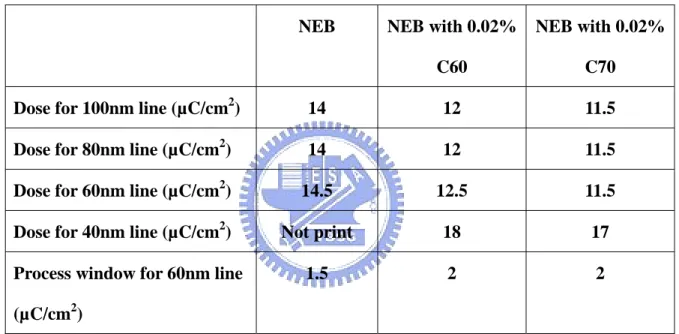
Table 3.1 . The dose and process window for the resists to print various designed lines.
Chapter 5
Table 5.1 Properties of the films annealed at 600 and 900 °C.
Chapter 6
Chapter 1
Introduction
1.1 Background
The progress of research into integrated circuits (ICs) is focused mainly on two goals: (1) increasing circuit performance (mainly by increasing circuit speed) and (2) increasing the functional complexity of the circuits. Scaling down device sizes is considered a very effective means of achieving these goals, but discovering technologies for achieving sub-60-nm contact holes is still a challenge [1]-[2].
The ITRS 2002 Update predicts that, for ASIC fabrication, the critical dimensions (CDs) for contact holes after etching will be required to be 65 and 45 nm by 2007 and 2010, respectively. Technologies that use chemical shrinkage for patterning sub-100-nm contact holes in resists have been reported previously [3]. In that report, the authors proposed using a polymeric shrinking agent that cross-links on the pattern’s sidewalls at a suitable mixing-bake temperature, but such a shrinkage technique faces the problem of defect formation in the resist pattern at higher mixing-baking temperature. Therefore, such chemical shrinkage technology has not been used previously for the generation of sub-60-nm features. Solving this problem, and to achieve the goal of preparing sub-60-nm contact holes in a silicon dioxide layer, requires controlling the shrinkage temperature for the ca. 90-nm contact holes in the resist and improving the etch process that allows further shrinkage to occur.
During the past two decades, there has been an extremely rapid growth in both the technology and the application of microelectronics, to the point that it now pervades virtually all aspects of commercial and military business. The size and performance of microelectronic devices has been improved substantially, especially in the past few years [4]-[5]. In the updated International Technology Roadmap for
Semiconductors, the 50 nm contact hole in the resist will be used in year 2011. The electron beam direct writing (EBDW), in comparison with optical lithography, is a promising means for controlling and patterning small features, down to sub-100nm [6]. This technology has a cost advantage for production volumes below 100 lots in the future [6]. In EBDW, the Gaussian beam has better resolution than shaped beam. But, the shaped beam has an at least 10-fold higher throughput than Gaussian beam due to imposing several pixels per shot [7]. In order to achieve the better resolution and high throughput for shaped beam technology, the utilization of thin resist film is inevitable [8]. However, the thin resist will face the challenge of poor etching resistance and serious line edge roughness. Nano-scale molecules are the possible means to solve the unaffordable etching resistance and enhance the lithographic performance for the thin resist film generation.
In the last few years, the industries focus on the planar CMOS scaling. However, scaling planar CMOS to short gate length will face many problems like electrostatics, excessive leakages, and mobility degradation. Non-planar CMOS MOSFETs provide potential advantages in packaging density, carrier transport, and device scalability [9]. SOI FinFETs technology has a lot of advantages such as the reduction of parasitic capacitances, the feasibility of diffusion resistors and capacitors free of junction effects, better device isolation leading to absence of latch up, substrate coupling and good gate control ability. But the floating body effect is a main problem of the SOI MOSFET devices. It will cause drain current “kink”, abnormal subthreshold slope, and low breakdown voltage [10]-[11]. The metal salicidation method has been used to suppress the floating body effect and DIBL [12]-[13] and reduce parasitic S/D resistances in the thin-film SOI devices.
Silicon technology has formed the basis of microelectronics and electronics systems for more than 30 years. In terms of productivity, the density of devices on a
silicon chip has followed Moore’s law, doubling about every two or three years since about 1980. Many researchers are interested in scaling down electronics devices so that they may perform at higher speeds and be prepared at lower costs. Conventional SiO2 gate dielectrics are reaching their physical thickness limit (1.5 nm); they cannot
be used as CMOS devices because the high direct tunneling current and poor reliability. For further scaling of devices, it has been proposed that SiO2 be replaced
by high-k dielectric constant materials, such as ZrO2, HfO2, Ta2O5, Al2O3, TiO2, and
silicates (ZrSixOy and HfSixOy) [14]–[21]. In fact, dielectric films having higher
permittivity allow the use of thicker films of equivalent electrical thickness as silicon dioxide; this situation will reduce the leakage current and improve the reliability of the dielectric films.
The most important properties of high-k dielectric materials that are necessary to maintain continuous increases in device performance and density are their low leakage current, low equivalent oxide thickness (EOT), high breakdown strength, high thermal stability, and gate electrode compatibility. The EOT, teq, of an alternative
high-k dielectric employ can be obtained from the simple equation
teq = (Kox / Khigh-k) thigh-k.
Where Kox and Khigh-k are the dielectric constants of silicon oxide and the high-k
dielectric, respectively, and thigh-k is the physical thickness of the high-k material.
Future downscaling will require high-k materials in which EOT values are reduced to nearly 0.7 nm [22]. We must bear in mind that many of the characteristics of these high-k dielectrics—such as their breakdown mechanism and hysteresis phenomena—are quite different from those of conventional silicon dioxide. When the gate dielectric materials experience high-temperature conditions (> 800 °C), the thermal stability of the high-k dielectric on silicon is an important issue that must be addressed for future MOSFET devices. The most suitable range of dielectric constants
is between 20 and 40. If the material has an extremely high k-value (> 80), it will induce a large fringing effect. For the purposes of achieving a low leakage current, it is desirable to choose a dielectric material that possesses a large band gap energy and a large band offset with respect to the Si substrate. ZrO2 has a dielectric constant of 25,
a wide band gap, good thermal stability, a high hardness, a high melting point, chemical hardness, and a high refractive index.
Recently, numerous technologies have been developed for the preparation of various high-k films [23]-[25]. To prepare insulating thin films, atomic layer deposition (ALD), physical vapor deposition (PVD), and chemical vapor deposition (CVD) methods have all been used to prepare films for new technologies. In the ALD process, ZrCl4 and H2O are used to prepare the ZrO2 films. For the PVD process, a
zirconium metal target is used for sputtering under ambient oxygen to deposit the ZrO2 films. In the CVD method, ZrCl4 precursor is used to deposit ZrO2 films. The
sol–gel method is a very interesting simple technique for preparing ceramic films [27]-[31].
1.2 Motivation
In this thesis, we investigate chemical shrinkage process parameters that are used in conjunction with electron beam lithography for preparing contact holes during ASIC fabrication. We have evaluated the various bake processes and process stabilities, and we discuss the cross-sectional images of holes formed by the chemical shrinkage process at various mixing temperatures. Upon completing the chemical shrinkage procedure, we also evaluated a series of dry etch recipes for the silicon dioxide layer.
technology, the utilization of thin resist film is inevitable. However, the thin resist will face the challenge of poor etching resistance and serious line edge roughness. Nano-scale molecules are the possible means to solve the unaffordable etching resistance and enhance the lithographic performance for the thin resist film generation. The molecules can be incorporated into the resist to alter its performance. The use of fullerene molecules possesses the advantage of extremely small and monodisperse. In our study, the sensitivity curve of resists after spiking with C60 and C70 molecules are investigated. The film stress, etch resistance and the effect of shaped electron beam dose on the contact hole sizes are carefully studied. In addition, the titanium nitride gap-filling and step coverage on contact holes by 0.02% w/v C70-incorporated resists are also evaluated.
Plasma treatment has long been used in TFT devices. The suitable plasma treatment can improve the electrical characteristics of the TFT devices because it can repair the defects in the devices. However, plasma treatment has not been proposed in the nano-SOI FinFETs fabrication. In this paper, we propose the 50nm gate length nano-SOI FinFETs with deep Ni-salicidation and NH3 plasma treatment. This is the
first time to apply NH3 plasma treatment on thin-film SOI devices. The NH3 plasma
treatment is expected to repair the process-induced defects in thin-film SOI devices. The sol–gel method can provide colloidal solvents or precursor compounds when metal halides are hydrolyzed under controlled conditions. In the sol–gel process, hydrolysis, condensation, and polymerization steps occur to form metal oxide networks. These reactions play fateful roles in modifying the final material’s properties. The most interesting feature of sol–gel processing is its ability to synthesize new types of materials that are known as “inorganic–organic hybrids.” The film formation with spin-coating is a simple method than ALD, PVD or CVD due to its cheaper precursor and tool. In addition, the film can be fabricated in the normal
pressure system instead of high vacuum system. Typically, ZrO2 is an excellent
heat-resistant and chemically durable material that is used, for example, as a material for furnaces [19]. Although ZrO2 generally provides good electrical insulation, no
reports exist that describe the electrical insulation properties of sol–gel-derived ZrO2
ultrathin film. In this thesis, we used the different annealing conditions on the sol–gel ZrO2 ultrathin films on silicon. The resulting material properties and electrical
performance of these deposited films were also evaluated by various characterization techniques.
In this paper, we use the sol-gel spin coating method to fabricate three SONOS-type flash memory devices. One is used HfO2 as charge trapping layer, and
one of the other two is hafnium silicate nanocrystal memory. We use sol-gel method to combine three high-k precursors, i.e. HfCl4, ZrCl4 and SiCl4 together to form
hafnium silicate and zirconium silicate co-existed in a memory device for the first time.
1.3 Thesis Organization
We will developed a fabrication technique, comprising electron-beam writing, chemical shrinking, and silicon dioxide etching, for the fabrication of sub-60-nm contact holes in chapter 2. Then, in the chapter 3, we will incorporate the fullerene molecules in the commercial electron beam resist to investigate the performances for patterning and filling the contact holes at nanometer scale. In the chapter 4, we will fabricate 50nm gate length nano-SOI FinFETs with deep Ni-salicidation and NH3 plasma treatment. Next in chapter 5, we will developed a simple method,
including a sequence of ZrCl4 precursor preparation under ice bath, sol-gel
ZrO2 ultrathin films. Finally in chapter 6, we fabricate a very simple and cheap
sol-gel spin coating method, together with RTA, to fabricate three different SONOS-type memories, such as HfO2 charge trapping layer memory, hafnium
silicate nanocrystal memory, and coexisted hafnium silicate and zirconium silicate nanocrystal memory.
Chapter 2
Fabrication of Sub-60-nm Contact Holes in
Silicon Dioxide Layers
2.1 Introduction
The progress of research into integrated circuits (ICs) is focused mainly on two goals: (1) increasing circuit performance (mainly by increasing circuit speed) and (2) increasing the functional complexity of the circuits. Scaling down device sizes is considered a very effective means of achieving these goals, but discovering technologies for achieving sub-60-nm contact holes is still a challenge [1,2].
The ITRS 2002 Update predicts that, for ASIC fabrication, the critical dimensions (CDs) for contact holes after etching will be required to be 65 and 45 nm by 2007 and 2010, respectively. Technologies that use chemical shrinkage for patterning sub-100-nm contact holes in resists have been reported previously [3]. In that report, the authors proposed using a polymeric shrinking agent that cross-links on the pattern’s sidewalls at a suitable mixing-bake temperature, but such a shrinkage technique faces the problem of defect formation in the resist pattern at higher mixing-baking temperature. Therefore, such chemical shrinkage technology has not been used previously for the generation of sub-60-nm features. Solving this problem, and to achieve the goal of preparing sub-60-nm contact holes in a silicon dioxide layer, requires controlling the shrinkage temperature for the ca. 90-nm contact holes in the resist and improving the etch process that allows further shrinkage to occur.
In this paper, we investigate chemical shrinkage process parameters that are used in conjunction with electron beam lithography for preparing contact holes during
ASIC fabrication. We have evaluated the various bake processes and process stabilities, and we discuss the cross-sectional images of holes formed by the chemical shrinkage process at various mixing temperatures. Upon completing the chemical shrinkage procedure, we also evaluated a series of dry etch recipes for the silicon dioxide layer.
2.2 Experimental
Table 2.1 lists the experimental flows and parameters used for preparing the sub-60-nm contact holes in the silicon dioxide layer. Electron beam exposure was performed on a Leica Weprint 200 stepper. The silicon dioxide layer was grown by wet oxidation using a mixture of hydrogen (8000 cm3/min) and oxygen (4999 cm3/min) gases at 978 °C in a low-pressure furnace. The electron beam energy was 40 keV, the beam size was 20 nm, and the exposure dose was 14 µC/cm2
. The developer for the JSR positive electron beam resist (MES-1EG) was an aqueous 2.38% tetramethylammonium hydroxide (TMAH) solution. A positive-tone electron beam resist was spin-coated on a silicon wafer (150 mm diameter) and baked at 110 °C for 120 sec. The thickness of the resist film was ca. 650 nm. After exposure and a post-exposure bake (110 °C for 120 sec), the wafer was developed using the TMAH solution. Again, a hard-bake was applied to the wafer (110 °C for 120 sec). A chemical shrinkage procedure was then applied. The chemical shrinking agent (AZ R-200, Clariant) was coated over the resist pattern, and the wafer was again soft-baked. The film thickness was ca. 400 nm. A mixing-bake step at 110 °C for 70 sec was then undertaken. The chemical shrinking agent reacted with the resist acid that diffused from the resist pattern. A cleaning step, using AZ R-2, which can wash away unreacted materials, was applied to the process. A hard-bake step was
performed at 110 °C for 2 min. Finally, we applied a plasma process using a mixture of CHF3 and CF4 gases to etch the underlying silicon dioxide layer. Critical
dimensions were evaluated using either an in-line scanning electron microscope (SEM, Hitachi S-6280) or a cross-sectional SEM (Hitachi S-4000).
2.3. Results and Disussion
2.3.1 Chemical shrinkage processes for the electron-beam
resist
As has been reported previously [3], the mixing-bake temperature and time are the critical factors for fabricating sub-100-nm contact holes in a resist when using the chemical shrinkage technique. Basically, the residual acid in the resist pattern diffuses into the side-wall regions of the shrinkage agent, which leads to cross-linkage reactions of the shrinkage agent. The extent of hole shrinkage in the positive resist depends upon the intrinsic acid diffusion behavior, such as its diffusion coefficient, and the time. Figure 2.1 illustrates the effect of mixing-bake temperature on the CDs of various contact holes for the positive E-beam resist. Characterization using top-down SEM clearly indicates that the CDs of contact holes at any size gradually narrow as the mixing-bake temperature is increased from 100 to 120 °C. An initial hole size of 140 nm formed by electron-beam patterning is suitable for shrinking down to the sub-100-nm level. We evaluated the profile of the contact holes at various mixing-bake temperatures by using cross-sectional SEM. The SEM pictures in Fig. 2.2 clearly illustrate the profile of the contact holes. Initially (prior to applying the chemical shrinkage agent), the contact holes have vertical sidewalls and a smooth surface. After a 105°C mixing-bake (subsequent to applying the chemical shrinkage agent), the sidewalls and surface covered with shrinkage agent appear to be slightly
distorted. When the mixing-bake temperature was increased to 110 °C, the contact holes remain open, but we observe an overhang effect in the contact holes formed after heating at either 115 or 120 °C. We attribute this finding to the effect of thermal flow of the shrinkage agent on the resist’s sidewalls at higher bake temperatures. This type of defect is not observed when viewing from by SEM from above the surface, but is very apparent from the cross-sectional SEM image. Clearly, the upper limit of the mixing-bake temperature for the chemical shrinkage technique is 110 °C.
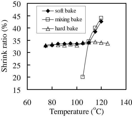
Figure 2.3 demonstrates the effect of mixing-bake times on the CDs of various contact holes for the positive resist at 110 °C. We observe that the hole dimensions decrease rapidly during the first 60 sec, but then gradually reach a plateau. Therefore, we believe that the optimal time for the mixing-bake process in this study is 70 sec. The reason for this trend with respect to mixing-bake time is that the process is dependent on the abundance of diffusion acid in the resist pattern, which is limited. If the amount of acid in the resist is increased, the CD will become narrower. The initial 140-nm hole formed by electron-beam patterning is the only one of the holes that we have studied that is suitable for being shrunk down to a sub-100-nm hole. Next, we compare the effects of the soft-bake, mixing-bake, and hard-bake processes after applying the chemical shrinkage agent. The control conditions for soft-baking, mixing-baking, and hard-baking are 85 °C for 70 sec, 110 °C for 70 sec, and 110 °C for 2 min, respectively. Figure 2.4 clearly indicates that the hard-bake temperature has no significant effect on the hole shrinkage ratio. The soft-bake temperature does have a significant effect above 110 °C, which we ascribe to the thermal flow effect discussed earlier. Among these baking processes, the mixing-bake temperature exhibits the most significant effect on the hole shrinkage ratio.
The hole shrinkage mechanism is closely dependent on the abundance of residual acid in the resist pattern. We exposed the wafer in the cleanroom environment (class
10) after initial contact hole definition for various delay hours. Figure 2.5 indicates that the shrinkage ratio fluctuates between 33 and 34% after various delay times. Although not illustrated here, the SEM images for these holes taken from above are very similar. It has been reported in the literature that a chemically amplified resist is sensitive to the molecular base, and leads to T-top and footing problems for the positive resist when not immediately developed (post-exposure delay)[4]. The molecular base in the cleanroom might have reacted to some extent with the surface acid. Most acids under the resist film, however, are not influenced by the molecular base from the air in the cleanroom. Therefore, the diffusion of the acids out of the resist still occurs during the mixing-bake process and the delay time has no effect.
2.3.2 Fabrication of 53-nm contact holes
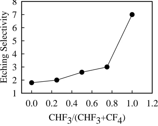
The fabrication of sub-60-nm contact holes in a silicon dioxide layer by the chemical shrinkage technique has not been reported previously. To ensure the applicability to nano-fabrication techniques, the resist should tolerate the etching process. Figure 2.6 depicts the etch selectivity that we estimate from the ratio of the plasma etch rates of silicon dioxide and the positive resist under various mixtures of gases. The selectivity gradually increases upon increasing the ratio of CHF3 from 0 to
0.75, and then increases abruptly upon a further increase in the gas ratio to 1. It has been suggested in the literature [5] that oxygen byproducts formed during silicon dioxide etching can react with carbon residues, especially at fluorine/carbon ratio < 2. Hence, the polymer formation blocks any further etching process.
The positive resist (650 nm thick) was coated onto a wafer upon which a silicon dioxide film had been grown. A variably shaped electron beam was used to pattern a 140-nm hole in the positive resist (Fig. 2.7a). The chemical shrinkage process was
then undertaken by spin-coating the shrinkage agent onto the resist pattern, followed by a soft-bake at 85 °C for 70 sec. The wafer was then subjected to a mixing-bake at 110°C for 70 sec. The residual acid diffuses out from the resist pattern into the shrinkage agent, which leads to acid-induced cross-linkage reactions taking place. After washing off the unreacted shrinkage agent and baking again at 110 °C for 2 min, the contact hole in the resist layer now has a 93-nm diameter (Fig. 2.7b). At the stage, the shrinkage ratio is ca. 33.6%. After the resist pattern had shrunk, the wafer was sent for plasma etching to fabricate a contact hole. Interestingly, the dimension of the contact hole in the silicon dioxide is not 93 nm: Figure 2.8 indicates that the hole size is 53 nm. The total shrinkage ratio of the hole diameter after the chemical shrinkage and plasma etch processes is 62.1%. What happens to the contact holes in the silicon dioxide layer during the plasma etch process? The sidewall deposition of residual polymers during the plasma etch process plays a significant role in narrowing the contact hole dimensions.
The etch mechanism for contact hole fabrication in a silicon dioxide layer is very complicated, with the dimensions of the pattern formed during the etch process being controlled by a balance between the amount of polymer deposited and the etch conditions. Explanations have been proposed in the literature [6-9] regarding micro-loading and aspect ratio-dependent etching (ARDE) to explain the observations made during etch processes. Micro-loading describes the variations of the etch rate between areas having different pattern densities, with features in low-pattern-density areas etching faster than features in high-pattern-density areas. Effects that are due to the pattern dimensions, which includes effects related to transport of etchant species into the pattern, or transport of etch products out of the pattern, are generally referred to as ARDE. Table II lists a series of data for the contact holes obtained after the chemical shrinkage and dry etch processes. The smaller holes exhibit a higher
shrinkage percentage for the etch process than the larger holes. We attribute this observation to the pattern dimension effect. As the pattern size is reduced, the probability for the flux of incoming polymer species to interact with the sidewall of the contact hole increases. Figure 2.9 depicts the relationship between the ratio of the hole dimension before and after etching and the ratio of the hole perimeter to the hole area of these nano-scale contact holes. We find that a linear dependence exists for the series of holes studied. This finding suggests the pattern reduction arising from sidewall polymer deposition during the etch process has an inverse relationship to the pattern diameter. The probability of transportation of a polymer species onto the sidewall of a contact hole is related linearly to the inverse of the contact hole size (after chemical shrinking). As a consequence, the contact hole in the silicon dioxide layer becomes smaller than expected after the etching process. We estimate that the uniformities (1 sigma) of the proposed method for contact hole formation after the processes of lithography, chemical shrinkage, and plasma etching are 3.21, 3.16, and 2.76 nm, respectively.
2.4 Summary
We have established a successful fabrication technique for preparing sub-60-nm contact holes in a silicon dioxide layer by electron-beam lithography. We have discussed in detail the many factors that influence the performance of the shrinkage process, such as the mixing-bake temperature, mixing-bake time, and hole dimensions before and after chemical shrinkage. Using this chemical shrinkage technique (mixing-bake of 110 °C for 70 sec) and an etch gas of CHF3/CF4 (1:1), we obtained a
minimum hole dimension of 53 nm. This technology meets the requirements2 for contact hole fabrication in the year 2009. We propose that a nano-hole effect occurs
during the etch-assisted shrinkage reaction because smaller holes have a higher percentage of polymer deposition in the resist sidewall than do larger holes.
Table 2.1 Process conditions for the fabrication of sub-60-nm contact holes in a silicon dioxide layer.
Oxidation Processes
Oxidation temperature 978°C, SiO2 thickness 150 nm
Gas components H2 (8000 cm3/min)/O2 (4999 cm3/min)
Lithography Processes
Spin speed 2500–5000 rpm, 30 sec
Resist thickness 650 nm
Exposure dose 14 µC/cm2 soft-bake 110°C, 120 sec Post-exposure bake 110°C, 120 sec
Development TMAH, 60 sec
Hard-bake 110°C, 120 sec
Chemical Shrink Processes
Soft-bake 85°C, 70 sec Mixing-bake 110°C, 70 sec
AZ remover (R-2) 10% IPA and 90% H2O, two puddles 40s/20s
Hard-bake 110°C, 120 sec Etch and Resist Stripping Processes
Etch time 60 sec
Gas components CF4, 20 sccm/CHF3, 20 sccm
Table 2.2 The diameters of contact holes formed after the processes of chemical shrinkage and plasma etching in SiO2, and their ratios (R = hole radius).
Hole diameter after chemical shrinkage
(x)
Hole diameter after dry etching in SiO2
(y)
y/x (percentage) Perimeter/area (2πR/πR2) 246 nm 233 nm 94.7% 0.0163 149 nm 128 nm 85.9% 0.0268 133 nm 98 nm 73.6% 0.0301 119 nm 79 nm 66.6% 0.0336 93 nm 53 nm 53.3% 0.0430
Temperature (
o
C)
95
100 105 110 115 120 125
C.D. (nm)
50
100
150
200
250
300
350
140 nm 180 nm 240 nm 360 nmFigure 2.1 Dependence of various mixing-bake temperatures for 70 sec on the critical dimensions (CDs) of contact holes formed by the chemical shrinkage technique. The initial hole sizes were 140, 180, 240, and 360 nm, respectively; top-down SEM was used to measure CD.
120oC
115oC
110oC
105oC
initial
Figure 2.2 Cross-sectional SEM image of contact holes in the resist after various mixing-bake temperatures.
Time (s)
20
40
60
80
100 120 140
C.D. (nm)
80
120
160
200
240
280
320
140 nm 180 nm 240 nm 360 nmFigure 2.3 Dependence of various mixing-bake times on the CDs of contact holes formed by the chemical shrinkage technique. The initial hole sizes were 140, 180, 240, and 360 nm, respectively; top-down SEM was used to measure CD.
15
20
25
30
35
40
45
50
60
80
100
120
140
Temperature (
o
C)
S
h
ri
n
k
ra
ti
o
(%
)
soft bake
mixing bake
hard bake
Figure 2.4 The effects of the various bake processes and temperatures on the shrinkage ratios of the contact holes.
igure 2.5 The effect of delay time on the shrinkage ratio (delay time = the period of
Delay time (hour)
0
5
10
15
20
25
30
Shrink ratio(%)
32.0
32.5
33.0
33.5
34.0
34.5
35.0
Ftime between the formation of the initial hole in the resist and the application of the shrinkage agent).
CHF3/(CHF3+CF4)
0.0 0.2 0.4 0.6 0.8 1.0 1.2
Etching Selectivity
1
2
3
4
5
6
7
8
(a)
Figure 2.8 (a) 53nm contact hole in SiO2 layer without resist stripping (image from
Figure 2.8 (b) 53nm contact hole in SiO2 layer after resist stripping (image from
p-down SEM).
(b)
53 nm
(c)
Figure 2.8 (c) 53nm contact hole in SiO2 layer after resist stripping (image from
tching and the ratio of the hole perimeter to hole area during the etching of the ano-scale contact holes.
y = -16.215x + 1.234 40% 60% 80% 100% 0.00 0.01 0.02 0.03 0.04 0.05
(hole perimeter) / (hole area)
(h o le d iameter a fter e tc h ) / ( h o le d iame te r b ef o re etch )
Figure 2.9 Linear dependence between the ratio of the hole dimension after and before e
Chapter 3
Resist Nano-modification Technology for
Enhancing the Lithography and Etching
Performance for Nano Contact
Hole and Line
3.1 Introduction
During the past two decades, there has been an extremely rapid growth in both the technology and the application of microelectronics, to the point that it now pervades virtually all aspects of commercial and military business. The size and performance of microelectronic devices has been improved substantially, especially in the past few years [1,2]. In the updated International Technology Roadmap for Semiconductors, the 50 nm contact hole in the resist will be used in year 2011. The electron beam direct writing (EBDW), in comparison with optical lithography, is a promising means for controlling and patterning small features, down to sub-100nm [3]. This technology has a cost advantage for production volumes below 100 lots in the future [3]. In EBDW, the Gaussian beam has better resolution than shaped beam. But, the shaped beam has an at least 10-fold higher throughput than Gaussian beam due to imposing several pixels per shot [4]. In order to achieve the better resolution and high throughput for shaped beam technology, the utilization of thin resist film is inevitable [5]. However, the thin resist will face the challenge of poor etching resistance and serious line edge roughness.
resistance and enhance the lithographic performance for the thin resist film generation. The molecules can be incorporated into the resist to alter its performance. The use of fullerene molecules possesses the advantage of extremely small and monodisperse. Ishii et al. [6] have been used fullerene molecule (i.e., 5 wt% C60) to modify positive tone resist, and found the fullerene can enhance the 6% etching resistance and not alter the sensitivity. In addition, they claim the negative tone chemically amplified resist incorporated with 3 wt% C60 exhibits strong environmental stabilization in postexposure delay. In the latter report [7], they find the resist sensitivity is degraded by the C60 due to the dissolution-inhibiting effect. Dentinger and Taylor [8] spike 7.9 wt% C60 into poly(methylmethacrylate) resist, and the etching resistance is promoted 8% and 26% for CF4 and Cl2 plasmas, respectively. However, the use of 3-7.9 wt%
C60 in the resists and the deterioration of resist sensitivity elevate the fabrication cost and restrict the further application of this technology.
In this study, the sensitivity curve of resists after spiking with C60 and C70 molecules are investigated. The film stress, etch resistance and the effect of shaped electron beam dose on the contact hole sizes are carefully studied. In addition, the titanium nitride gap-filling and step coverage on contact holes by 0.02% w/v C70-incorporated resists are also evaluated.
3.2 Experimental
The fullerene molecules of C60 and C70 were purchased from Alfa Aesar Company. The toluene solvent was obtained from E. Merck (Darmstadt, Germany). The negative NEB-22 resist used in this study was obtained from SUMITOMO Chemical Co., Ltd. (Japan). The resist samples in this study have four types, named NEB, NEB+Toluene, NEB+C60, and NEB+C70, respectively. The NEB means the
NEB-22 resist without any modification. The “NEB+Toluene” means the mixture of 50mL NEB-22 resist and 50mL toluene solvent. For the “NEB+C60-0.01%” sample, the 0.01g C60 fullerene is first dissolved in 50mL toluene, and then mixes with 50mL NEB-22 resist. The final concentration of C60 molecule in the resist is 0.01% w/v. In the same manner, the “NEB+C70-0.02%” uses 0.02g C70 fullerene to prepare the sample.
And the DSE-1010 positive resist used in this study was obtained from DONGJIN Chemical Co., Ltd. (Korea). There are four types of resist samples in this study, named DSE, DSE + Toluene, DSE + C60, and DSE + C70, respectively. The DSE means the DSE-1010 resist without any modification. The “DSE + Toluene” means the mixture of 50mL DSE-1010 resist and 50mL toluene solvent. For the “DSE + C60-0.01%” sample, the 0.01g C60 fullerene is first dissolved in 50mL toluene, and then mixes with 50mL DSE-1010 resist. The final concentration of C60 molecule in the resist is 0.01% w/v. In the same manner, the “DSE + C70-0.02%” uses 0.02g C70 fullerene to prepare the sample.
Electron beam exposure was performed on a Leica Weprint 200 stepper. The electron beam energy was 40 keV, and the beam size was 20 nm. The developer for the electron beam resist was an aqueous 2.38% tetramethylammonium hydroxide (TMAH) solution. A electron beam resist was spin-coated on a silicon wafer (150 mm diameter) and baked at 95 °C for 120 sec. After exposure and a post-exposure bake (115 °C for 120 sec), the wafer was developed using the TMAH solution for 60 sec. Again, a hard-bake was applied to the wafer (115 °C for 120 sec). Critical dimensions were evaluated using either an in-line scanning electron microscope (SEM, Hitachi S-6280) or a cross-sectional SEM (Hitachi S-4000). The stress of resist film was measured by TENCOR FLX-2320 instrument. In the stress measurement, the curvatures of bare silicon wafers, resist-coated wafers were determined.
Silicon dioxide film was etched using a reactive-ion etcher (RIE, Tokyo Electron Limited, Model TE5000, Japan). There are two steps for silicon dioxide etching. The operating conditions for step 1 are- 0.2 Torr pressure, 0 W RF power, 400 cm3min-1 Ar gas, and etching gases of CHF3 and CF4 (CHF3+CF4=40 cm3min-1). The operating
conditions for step 2 are- 0.2 Torr pressure, 500 W RF power, 400 cm3min-1 Ar gas, and etching gases of CHF3 and CF4 (CHF3+CF4=40 cm3min-1).
The thermal oxide was grown under dry O2 at 900oC in quartz reactor to a
thickness of 100nm. After coating the fullerene-incorporated resist onto the thermal oxide and resist patterning, the plasma process of mixing CHF3 and CF4 gases was
used to etch the underlying silicon dioxide layer. Then, the contact holes defined by 0.02% w/v C70-incorporated resist were deposited with the titanium nitride (TiN) plug by physical vapor deposition (PVD) and chemical vapor deposition (CVD). The TiN PVD sputter system (ULVAC SBH-3308 RDE system) was used to deposit 200-nm TiN film, and argon and nitrogen were used as process gases. For the film deposition by CVD method, the tool from Materials Research Corporation (MRC) was used to deposit TiN film by gas mixture of TiCl4 and NH3 at 630 oC. The
chemical reaction is as follows: 6TiCl4 + 8NH3 → 6TiN + 24HCl + N2.
The other the polysilicon gates with spacer were fabricated with the 0.01% w/v C60-incorporated resist on 6 inch silicon wafer. First, the gate oxide was grown under dry O2 at 900oC in quartz reactor to a thickness of 1.5nm. After a 50nm poly-Si film
was deposited by low pressure chemical vapor deposition system (LPCVD) and doped by ion implantation, and then patterned to from a gate. The poly-SiGe is also deposited by LPCVD. A 50nm tetraethyl orthosilicate film was also deposited by LPCVD. The gate spacer was formed by reactive ion etching. Prior to remove native oxide before cobalt deposition, all wafers were dipped in the HF solution. The 5nm cobalt was deposited by physical vapor deposition system (PVD). The first annealing
step for the cobalt silicide (CoSi2) formation was operated at 550 oC in N2 ambient for
30 sec. The un-reacted cobalt was removed by selective wet etching in the mixture of H2SO4 and H2O2. The second step annealing step was performed at 750 oC in N2
ambient for 30 sec. For the nickel silicide (NiSi) formation, the wafer was deposited 5nm Ni by PVD. The annealing step used only one step for the sample was operated at 500 oC in N2 ambient for 30 sec. The un-reacted Ni was also removed by wet etching in the mixture of H2SO4 and H2O2.
3.3. Results and Discussion
3.3.1. Enhancement of lithographic performance
In the electron beam writing technology, the negative tone resist is usually used to fabricate the line or low density patterns, especially for the gate line. In this study, the commercial NEB-22 resist is a negative type, and the fullerene molecules such as C60 and C70 are incorporated into the commercial resist. Figure3.1(a) depicts the resist sensitivity curve. The dose (DC) for the “NEB” sample that the polymer
constituent begins cross-linkage is 5.2 µC/cm2, while the dose (DO) that the polymer
can achieve 100% cross-linkage is 6.2 µC/cm2. As to the “NEB+Toluene” sample, both the DC and DO are increased. This observation is attributed to the dilution of acid
generator in the sample, and therefore, reduces the sensitivity. Interestingly, the sensitivity for 0.01% w/v “NEB+C60” or “NEB+C70” sample is significantly enhanced after nano-material modification. Both the DC and DO are decreased to
4.6µC/cm2 and 5.4µC/cm2, respectively. This finding suggests that the incorporation of fullerene molecules into resist can effectively enhance the process throughput.
Another the electron beam writing technology, positive tone resist is usually used to fabricate the contact hole [3]. In this study, the commercial DSE-1010 electron
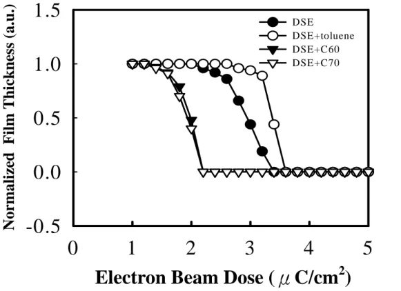
beam resist is a positive type, and the fullerene molecules such as C60 and C70 are incorporated into the commercial resist. Figure3.1(b) depicts the resist sensitivity curve. The irradiation dose (Di) for the “DSE” resist that the acid generator and
functional group in the polymer begins reaction is 2.3 µC/cm2, while the dose (Dc)
that the polymer film can fully dissolve is 3.4 µC/cm2. As to the “DSE+Toluene” sample, both Di and Dc are increased. This observation is attributed to the dilution of
acid generator by toluene solvent, and therefore, reduces the sensitivity. Interestingly, the sensitivity for 0.01% w/v “DSE+C60” or “DSE+C70” sample is significantly enhanced after spiking the fullerene molecules. Both Di and Dc are decreased to 1.4
µC/cm2 and 2.2 µC/cm2, respectively. This finding suggests that the incorporation of fullerene molecules into resist can effectively enhance the process throughput.
What happens to the decrease of addressing dose for the resist after spiking with fullerene molecules? In the resist, the electron beam activates the bond of acid generator to produce acid, and the acid induces the functional group reaction of the polymer. The irradiated electron beam easily penetrates through the void region embedded in the resist film, and degrades the throughput. We infer the fullerene molecules with sub-nanometer sizes (0.7-0.8 nm) are embedded into the void of resist sample (in Fig. 3.2) The C60 or C70 fullerene embedded in the void region has a higher electron affinity ~2.6 eV, and therefore, facilitate the bond activation for the acid generator. As we know the electron accelerating voltage can influence the sensitivity, the higher accelerating voltage can improve the resist resolution but deteriorate the resist sensitivity [4]. However, the incorporation of fullerene molecules can shorten the resist exposure time
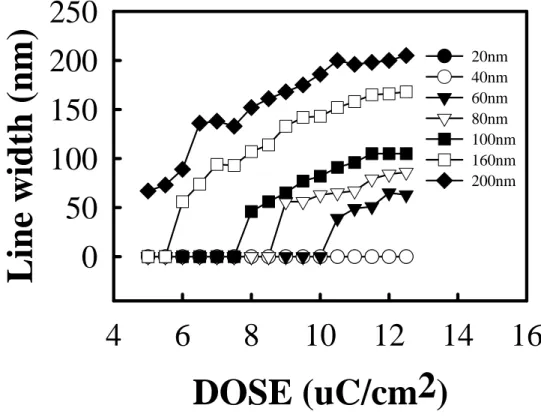
Figure3.3 indicates the line width increases with the exposure dose. We define the dose range for the “nominal line ± (10%)(nominal line)” as the process window. Table 3.1 suggests the fullerene-incorporated resist has wider dose window than
unadulterated resist. The resist with C60 modification in Fig. 3.3 can fabricate sub-50nm line with respect to C70. This phenomenon implies the C60 with smaller size is better for the resist void filling. The SEM images for the resist with 0.02% w/v fullerene modification are illustrated in Fig. 3.4. The print of sub-50nm lines can not achieve from Fig. 3.4a. The line without fullerene tends to pattern collapse at aspect ratio of 5.75 due to the insufficient adhesion at interface. Figure 3.4b demonstrates the resist without fullerene can resolve 53nm lines at aspect ratio of 4.3, but the line has serious line edge roughness problem. The line edge roughness can lead to higher leakage current for the future nano-devices. However, the resist with 0.02% C60 modification can print 46nm lines (Fig. 3.4c), and 0.02% C70 can print 51nm lines (Fig. 3.4d). The problem of line edge roughness is not seen for the resist with fullerene modification. This observation is dependent on the void of resist polymer of which is filled with fullerene. The fullerene on the sidewall also can minimize the extent of protrusion of polymer. In addition, the interfacial adhesion between fullerene-incorporated resist and the substrate is stronger than the unadulterated resist and the substrate.
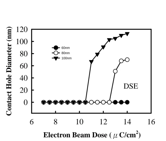
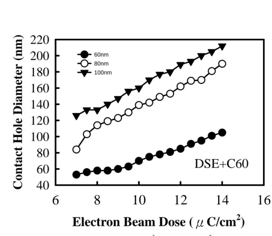
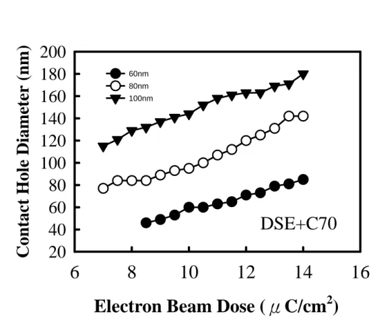
Figure 3.5a indicates the hole dimension is significantly influenced with the exposure dose, while the fullerence-incorporated resists in Fig. 3.5b and 3.5c are not. The resist without embedded fullerene molecules can not resolve 60 nm contact hole. The electron beam doses at 7 µC/cm2 and 8.5 µC/cm2 can resolve 50 nm contact hole for the resist with 0.01% C60 and C70 modification, respectively. We define the dose range for the “nominal hole ± 10% x (nominal hole)” as the process window. The fullerene-incorporated resists have wider dose windows (i.e. 8-9.5 µC/cm2 for 0.01% C60, and 9.5-11.5 µC/cm2 for 0.01% C70) for 60 nm contact hole formation than unadulterated resist. These phenomena are all attributed to the high electron affinity of fullerene molecules.
The C70 fullerene molecule is chosen for further studies due to its better process window. The SEM images for the resist with 0.01% w/v fullerene modification are illustrated in Fig. 3.6. The fabrication yield of 60 nm nominal hole in Fig. 3.6a is not satisfactory due to the lack of electron affinity fullerene. Figure 3.6b demonstrates the resist with C70 fullerene molecules can resolve 53 nm hole.
The stress for various fullerene-incorporated films is demonstrated in Fig.3.7. The resist film without spiking fullerene has large tensile stress. The spiking of fullerene molecules such as C60 or C70 can prevent the stress, and is beneficial for the surface flatness. The fullerene molecules can fill the void of resist and minimize the deformation as spin-coating the resist.
3.3.2. Enhancement of etching performance
In this study, we use RIE to evaluate the etching resistance for the fullerene-incorporated resist on a silicon dioxide layer. The feeding gas is a mixture of Ar, CHF3, and CF4. The etching rates of these resists and the oxide film both decrease
upon increasing the CHF3 content. This observation explains the role CHF3 in the
plasma. The species generated from CHF3 in the plasma are H+ and CF3-, and the CF3
-species can quench the activity of CF3+ in the plasma. Hence, the etching rate
decreases. Figure 3.8a depicts the etching selectivity for these resists. The selectivity gradually increases upon increasing the relative CHF3 content. And figure 3.8b
depicts the etching selectivity for these resists. The selectivity is defined as the etch rate of silicon dioxide film to the resist film. The selectivity gradually increases upon increasing the relative CHF3 content.
In addition, the increase of amount of fullerene molecules can also enhance the selectivity than the unadulterated resist. This observation supports the assumption that
the fullerene molecules can effectively fill the free volume of the resist film. The fullerene molecules consolidate the film, and therefore, the resist film is more resistance to the etching gases. We also find the incorporation of C70 has better etch resistance than C60. This finding is attributed to the higher molecular of C70. It should be noted that the amount of fullerene spiking is only 0.01-0.02%, and is quite low than literature [6-8] report (i.e. 3-50%).
The etching behavior of these resists on the polysilicon film is evaluated using an ECR etcher. The feeding gas is a mixture of Cl2 and O2. The etch rate of these resists
decrease upon increasing the amount of Cl2. This observation can be explained by
considering the relative amount of O2 in the plasma: a decrease in O2 ratio decreases
its reaction with the carbon-based ingredients of the resist. For the poly-Si film, the etching rate is very small as if the Cl2 ratio is below 0.8. However, it increases
abruptly at the ratio higher than 0.8. This finding indicates that an O2 ratio greater
than 0.2 is required to oxidize the poly-Si film quickly. The silicon dioxide that forms is resistant to Cl2 etching. Figure 3.9 depicts the etching selectivity for these resists.
The selectivity significantly increases upon increasing the Cl2 to higher than 0.8. In
addition, the increase of amount of fullerene molecules can also enhance the selectivity than the unadulterated resist. This observation also strengthens the role of fullerene molecules mentioned early.
3.3.3. Application of fullerene-incorporated resists for
nano-silicide gate and the electrical properties
The various metal silicided lines, such as self-aligned cobalt silicide (CoSi2)/poly-Si, nickel silicide (NiSi)/poly-Si, and NiSi/poly-SiGe, are fabricated
cobalt silicide line is depicted in Fig.3.10 The silicon nitride spacer, self-aligned cobalt silicide, poly-Si and the underlying silicon dioxide layer are successfully fabricated in the Kelvin structure. Then, the sheet resistance (in unit of Ω/sq) of the designed line is determined at probe station. Figure 3.11a illustrates the sheet resistance of CoSi2 has no significant difference in the range 100-200nm. However,
the resistance increases dramatically as the line narrowing than 100nm. The phenomenon has been reported to be linked with the presence of infrequent voids in narrow silicide lines [10]. As to the NiSi/poly-Si line in Fig. 3.11b, the sheet resistance gradually decreases with narrowing the line from 200nm to 60nm. However, the range of sheet resistance is only 0.7 Ω/sq, and is insignificance. The sheet resistance of NiSi/poly-Si is quit lower than CoSi2/poly-Si. This observation is
attributed to the lower Si content in the NiSi than in the CoSi2. The underlying poly-Si
of NiSi has changed to poly-SiGe for evaluating the electrical property. Figure 3.11c demonstrates the sheet resistance gradually increases with shrinking the line width. In addition, the electrical property of NiSi on poly-SiGe is deteriorated than on the poly-Si. We suppose the NiSiGe film is formed between the NiSi and poly-SiGe, and has lower Ni percentage.
3.3.4. Application of fullerene-incorporated resists for
patterning and filling the contact hole
Figure 3.12a depicts the 56 nm contact hole in the silicon dioxide film can be fabricated by 0.02% w/v C70 fullerene modification. The cross section SEM in Fig.3 12b suggests the surface diameter of the hole is wider than the bottom diameter of the hole due to reactive-ion plasma etching. The average aspect ratio for the contact hole is ~2. In order to evaluate the hole filling process of TiN plug, the PVD and CVD