國立交通大學
電子工程學系 電子研究所
碩 士 論 文
應用於通用圖形處理器上
具熱感知及位置相關之三維佈局規劃演算法
Location-Dependent Thermal-Aware 3D Floorplan on
General-Purpose GPU
研 究 生:謝明廷
指導教授:黃俊達 博士
應用於通用圖形處理器上
具熱感知及位置相關之三維佈局規劃演算法
Location-Dependent Thermal-Aware 3D Floorplan on
General-Purpose GPU
研究生:謝明廷 Student: Ming-Ting Hsieh
指導教授:黃俊達 博士 Advisor: Dr. Juinn-Dar Huang
國立交通大學
電子工程學系 電子研究所
碩士論文
A Thesis
Submitted to Department of Electronics Engineering & Institute of Electronics College of Electrical & Computer Engineering
National Chiao Tung University in Partial Fulfillment of the Requirements
for the Degree of Master of Science
in
Electronics Engineering & Institute of Electronics July 2013
Hsinchu, Taiwan, Republic of China
i
應用於通用圖形處理器上
具熱感知及位置相關之三維佈局規劃演算法
研究生:謝明廷 指導教授:黃俊達 博士
國立交通大學
電子工程學系 電子研究所碩士班
摘 要
隨著製程的演進,在縮小尺寸上遇到了瓶頸。因此三維堆疊技術被提出並使 用於延續摩爾定律(Moore’s Law)。因為三維堆疊令單位面積功率增加,產生了散 熱不易的現象,導致晶片過熱,這使得熱議題(thermal issues)無法被避免。熱 模 型 (thermal model) 被 廣 泛 應 用 在 熱 感 知 (thermal-aware) 佈 局 規 劃 (floorplan)。經由熱模型,我們可以知道熱的分佈情形;然而精確的熱模型因為 執行時間過長,不適合應用在佈局規劃上。然而簡化的熱模型雖然有快速的執行 能力,但喪失了精確度。因此我們在這篇論文裡提出一個兼顧快速、且可提供相 當程度精確性的熱模型。除此之外,我們提出兩種技術去預防潛在性熱點(hotspot) 的產生–斥力(repulsion force)法以及過熱保護區(over-heat prevention zone)機制。 經由這些方法,我們使佈局規劃裡的最高溫得到改善,以及令溫度分佈更為均 勻。
最後,我們把這個演算法應用在通用圖形處理器上(GPGPU)。藉由大量的核 心數去縮短執行時間。
ii
Location-Dependent Thermal-Aware 3D Floorplan on
General-Purpose GPU
Student: Ming-Ting Hsieh Advisor: Dr. Juinn-Dar Huang
Department of Electronics Engineering & Institute of Electronics
National Chiao Tung University
Abstract
As the development of integration technology, shrinking chip size has encountered bottlenecks. Three-dimensional (3D) integration is then proposed to continue sustaining Moore’s Law. However, due to the significant increasing of the stacking power, it is hard to dissipate heat by using 3D stacking structure. Therefore, the thermal issues become inevitable and has to be handled carefully.
In order to solve thermal issues, the thermal model is widely used in thermal-aware floorplan to mimic the temperature distribution. But the runtime of accurate thermal model is too long to be used in floorplan. On the other hand, the simplified thermal model is fast and suitable for floorplan, but it loses accuracy. As a result, in this thesis, we propose a fast thermal model, which also provides a considerably precise temperature estimation. Besides, we also propose two techniques to prevent potential hotspots, named repulsion force (RF) and over-heat prevention zone (OHPZ). By these methods, we not only reduce the maximum temperature but let temperature distribution be more uniform.
Finally, we implement this algorithm on GPGPU (General Purpose computing on Graphic Processor Unit). Runtime is reduced by using a great amount of cores.
iii
誌 謝
首先我要感謝我的指導老師-黃俊達教授。在老師細心的指導下,我學會了 面對問題的態度與解決的方法;老師總是抽空與我討論研究,並樂於給予我適當 的建議以及方向,好似一盞明燈,讓我在學術瀚洋裡不會迷失方向。也謝謝我的 口試委員陳宏明教授與黃婷婷教授,能撥冗參加口試。 再來要感謝我的父母,正因為有他們含辛茹苦地把我拉拔長大,我才能有今 日的成就,感激之情溢於言表。接下來要感謝實驗室的博班學長姐:卡拉學長教 會我平行化運算的使用方法,使得這份論文的後半部得以完成;形姐在碩一時對 我的指導,讓我受益良多;宏哥即使在百忙之中,也會抽空幫我解決 server 的 問題,以及以豐厚的經驗教導我各大國家的民族風情及軍事比較;特別要感謝莎 姐一直以來對我的指導,總能包容我拙劣的報告方式,認真聆聽我的想法,並給 予有用的意見與指教。 感謝實驗室的同學-包子、廣正、馬力、和鵬先,與你們一起修課、研究的 日子,是我最寶貴的經驗與回憶,沒有之一。也要感謝實驗室的學長們,由於有 學長們的研究成果,我這篇論文才得以順利完成;接下來"順便"感謝實驗室學 弟妹們:AJ、BJ、偉豪、慧珊、顥瀚、還有子敬,平時在面對壓力比研究及修課 還大的雜事,仍能坦然面對、果斷處理,讓我能在最舒適的環境裡做研究。 最後要感謝所有曾經幫助過我的人,因為你們,我的人生得以完整。iv
Content
摘 要... i Abstract ... ii 誌 謝... iii Content ... iv List of Tables ... viList of Figures ... vii
Chapter 1 Introduction ... 1 1.1 3D Integrated Circuits ... 1 1.2 Floorplan ... 3 1.2.1 2D Floorplan ... 3 1.2.2 From 2D Floorplan to 3D ... 4 1.2.3 Related Work ... 5 1.3 GPGPU ... 6 Chapter 2 Preliminaries ... 9 2.1 Thermal Model ... 9
2.1.1 Compact Resistive Thermal Model ... 9
2.1.2 Z-Tile ... 10
2.2 Motivation ... 11
2.3 Problem Formulation ... 14
Chapter 3 Thermal-aware Floorplan Algorithm ... 15
3.1 Proposed Thermal Model ... 15
3.2 Proposed Thermal-aware Floorplan Algorithm ... 17
3.2.1 Repulsion Force ... 19
3.2.2 Over-heat Prevention Zone ... 21
Chapter 4 Parallel Floorplan Algorithm on GPGPU ... 23
4.1 Parallel Floorplan – Area ... 24
4.2 Parallel Floorplan – Wirelength and TSV Count ... 26
4.3 Parallel Floorplan – Temperature ... 26
4.3.1 Power Density Evaluation... 26
4.3.2 Temperature Evaluation ... 27
4.4 Parallel Floorplan – Repulsion Force ... 28
Chapter 5 Experiments ... 29
5.1 Environmental Setup ... 29
5.2 Experimental Results ... 31
v
5.2.2 Runtime ... 34 Chapter 6 Conclusion ... 38 Reference ... 39
vi
List of Tables
Table 1. Comparison with shared and global memory. ... 8
Table 2. Thermal-electrical duality [33]. ... 10
Table 3. Benchmarks. ... 30
Table 4. Physical settings. ... 30
Table 5. Experimental results – n100. ... 32
Table 6. Experimental results – n200. ... 32
Table 7. Experimental results – n300. ... 32
Table 8. Runtime – n100. ... 35
Table 9. Runtime – n200. ... 35
vii
List of Figures
Figure 1. Relative delay vs. feature size [1]... 1
Figure 2. Global interconnects before and after 3D integration. ... 2
Figure 3. Wire bonding technology [8]. ... 2
Figure 4. Through-silicon vias (TSVs) technology. ... 3
Figure 5. (a) Slicing and (b) non-slicing floorplan. ... 4
Figure 6. Thread batching. ... 7
Figure 7. Structure. ... 8
Figure 8. Compact resistive thermal model. ... 9
Figure 9. Construction of Z-tile model. ... 11
Figure 10. temperature produced by module placed at (a) corner (b) center. ... 12
Figure 11. Heat distribution of chip. ... 13
Figure 12. Temperature vs. harmonic mean. ... 13
Figure 13. Thermal resistance evaluation. ... 17
Figure 14. Algorithm flow. ... 18
Figure 15. Temperature distribution ... 21
Figure 16. Modules are placed by using SP representation. ... 22
Figure 17. Tree reduction technique. ... 26
Figure 18. Experiments flow... 29
Figure 19. Thermal data – n100. ... 32
Figure 20. Thermal data – n200. ... 33
Figure 21. Thermal data – n300. ... 33
Figure 22. Thermal data II – n100. ... 34
Figure 23. Thermal data II – n200. ... 34
Figure 24. Thermal data II – n300. ... 34
1
Chapter 1 Introduction
1.1 3D Integrated Circuits
Nowadays, under nano-scale technology, high transistor density makes chip more complicated. However, as the technology progressing with shrinking size of device, it is difficult to continue shrinking size of device because of physical limitations. Many challenges incurred at the same time with the feature size getting smaller, such as power dissipation, reliability, leakage power, clock distribution, and yield issue [1]. Moreover, smaller feature size causes the delay of global interconnects becomes much longer than the delay of gates, as shown in Figure 1. Hence, interconnect delay becomes more important.
Gate Delay (Fan out 4) Local (Scaled) Global with Repeaters Global w/o Repeaters 100 10 1 0.1 250 180 130 90 45 32
Process Technology Node (nm)
R e la ti ve D e la y
Figure 1. Relative delay vs. featuresize [1].
In order to solve above problems, three dimensional integrated circuit (3D IC) emerges and has been discussed in recent years [3]-[7]. By stacking dies, footprint area becomes smaller, which implies transistor density gets higher. Moreover, global interconnect length get shorter by vertical transmission, as shown in Figure 2. Shorter global interconnect length bring some benefits, such as lower power dissipation and shorter global interconnect delay.
2
A
B
C
D
E
F
B
C
F
A
D
E
Figure 2. Global interconnects before and after 3D integration.
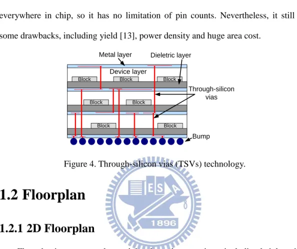
Due to the dies stacked, dies need to communicate each other in vertical direction. There are two ways to accomplish such inter-layer communications [3][4], the wire bonding [3] and through-silicon vias (TSVs) technology [4] as shown in Figure 3 and Figure 4 respectively.
Wire bonding technology is usually used for system-in-package (SiP). Since the devices communicated by outside wires, as shown in Figure 3, it takes a long communication path to connect devices between different layers. And these kinds of technologies has limitation of number of pins.
Figure 3. Wire bonding technology [8].
The other technology is through-silicon vias (TSVs) technology as shown in Figure 4. Devices residing in different layers communicate each other by TSVs which transmit signal vertically. Compared to wire bonding technology, TSV technology
3
brings some benefits, such as shorter global interconnects [9]-[12], smaller footprint area [13], lower interconnect power [14] and better heterogeneous integration. Besides, the major advantage of TSV technology is that TSVs can be placed everywhere in chip, so it has no limitation of pin counts. Nevertheless, it still has some drawbacks, including yield [13], power density and huge area cost.
Block Block Block
Block Block Block Block Metal layer Device layer Dieletric layer Bump Through-silicon vias
Figure 4. Through-silicon vias (TSVs) technology.
1.2 Floorplan
1.2.1 2D Floorplan
Floorplan is to arrange the module whose data are given, including height, width, power density, and netlist, for some optimization goals, for instance, area and wirelength. In floorplan, there are two major components. One is representation, which represent the floorplan. We can know the location of modules in floorplan by representation. The other one is approach method.
4
(a) (b) Figure 5. (a) Slicing and (b) non-slicing floorplan.
Representation is mainly divided into two categories - slicing and non-slicing as shown in Figure 5. Slicing floorplan can be sliced into two parts iteratively until each part contains only one module, where the slicing cut can be horizontal or vertical. Normalized polish expression [15] and slicing tree [16] are floorplan representations which use slicing procedure to handle the floorplan. The other one is non-slicing floorplan, that is to say, it cannot be sliced into two parts always, b*tree [17], sequence pair [18], and O-tree [19] are this kind of floorplan representation.
After the representation of the floorplan is ready, the next step is to obtain a good floorplan under the varied goals defined by the designer. In general, two methods are used widely, simulated annealing (SA) method and analytical approach. SA method performs a series of perturbations changing the representation to get the new one. This method accept the worse result with certain probability. SA method can get out of local optimum by accepting worse result. The analytical approach gets the solution by using the mathematical formulation with constraints. The quality of floorplan is determined by cost during floorplan processing. The cost is multi-object combination, like area, wirelength and so on.
1.2.2 From 2D Floorplan to 3D
From 2D to 3D, there are some benefits in floorplan such as smaller footprint area and shorter wirelength, as shown in Figure 2. However, there are also some extra
5
issues. First of all, TSV is an extra issue we must to consider. [1] mentions the size of TSV is 1024 times larger than size of 6-transistor SRAM. Therefore, the less the TSV count, the better the area of floorplan. So the first issue is to minimize TSV count.
Next, due to the stacked dies, the heat dissipation path is longer, except the layer nearest the heat sink. The heat is more difficult to dissipate, so the heat dissipation issue gets more important.
In 3D floorplan, we still have to consider the issues of 2D floorplan. Additional, we must consider extra issues from 3D stacked. Hence, the cost includes not only the issues of 2D floorplan but also the problems brought by 3D stacked.
1.2.3 Related Work
In 3D floorplan, there are extra issues we should consider. [20][21] consider the relation between TSV count and wirelength. In general, TSV count is the minimization goal.
There are several way to deal with heat dissipation issue. [22]–[28] redistribute whitespace by module shifting. [22]–[26] shift the module to insert the thermal via which does not transmit signal. Thermal via is helpful to dissipate heat because of its high thermal conductivity. [27][28] consider the power density of module, and let more whitespace be around the module with higher power density. These methods for handling thermal issue are post-processing after SA procedure finished. Quality of these methods will highly depend on the solution SA procedure produced.
The other way to consider thermal issue is evaluate temperature of chip during SA procedure [29][30]. This method will calculate temperature as cost function in each perturbation. However, because there are a lot of perturbations in SA procedure, the method of evaluating temperature cannot be too complex. Thus, Cong et al. [29] proposed a simplified thermal model which evaluates temperature fast.
6
1.3 GPGPU
GPGPU, the abbreviation of “General Purpose computing on Graphic Processor Unit”, means using graphic processor unit (GPU) to perform computation which is traditionally handled by central processing unit (CPU). Owing to powerful parallel processing capabilities of modern graphic processor and programmable pipeline, GPU can deal with non-graphical data. Because the core count of GPU is much more than CPU, GPU has better performance when performing a lot of data, especially in single instruction multiple data (SIMD).
GPU originally deals with image processing including a large amount of floating point operations, so GPU is good at operating floating point. However, it’s not skilled in operating branch instruction.
Compute unified device architecture (CUDA), which is created by NVIDIA [31], is one of parallel computing and programming platforms. Basically, CUDA is divided into two parts, software and hardware. In software side, when a CPU calls a kernel function, it determines the number of blocks and number of threads per block as shown in Figure 6. In CUDA, a block consists of a set of threads, and a thread represents the minimum operation unit. Different kernel functions can determine respective number of blocks and threads .After determining the number of blocks and threads, the GPU processes the instruction on threads in parallel. This concept is so-called single instruction multi threads (SIMT).
7
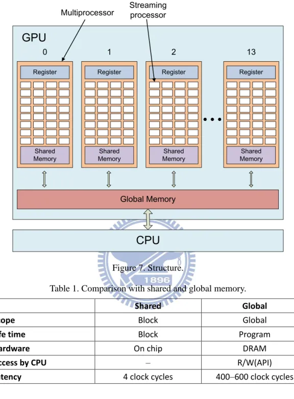
Figure 6. Thread batching.
In hardware side, the GPU contains several multiprocessors, where many streaming processors reside, as shown in Figure 7. The block and thread we have introduced before will map to the multiprocessor and streaming processor respectively. Thus, even though there are hundreds or thousands of threads, the number of threads which can simultaneously operate depends on number of streaming processor by user. However, there are fewer dividers in each multiprocessor. If a kernel function operates division, the number of threads which operate simultaneously is determined by number of dividers, not number of streaming processors.
Figure 7 also illustrated 2 types of memory units utilized by CUDA, shared memory and global memory. Each multiprocessor has one shared memory, and the shared memory can be used by multiprocessor where shared memory locates. That is, threads on same block can use shared memory to save/load data. If communication between different multiprocessors or GPU and CPU, these conditions use global memory. Comparison of two memory units is shown in Table 1.
Because the latency of global memory is much longer than shared memory, more than one hundred times, the using of global memory must to be avoided as possible. Nevertheless, shared memory will be clear as kernel function is end, so if there are some data other kernel functions will use, these data have to save at global memory.
8 Register Shared Memory 0 Register Shared Memory 1 Register Shared Memory 2 Register Shared Memory 13 ● ● ● Global Memory Multiprocessor Streaming processor
GPU
CPU
Figure 7. Structure.
Table 1. Comparison with shared and global memory.
Shared Global Scope Block Global
Life time Block Program
Hardware On chip DRAM
Access by CPU – R/W(API)
9
Chapter 2 Preliminaries
2.1 Thermal Model
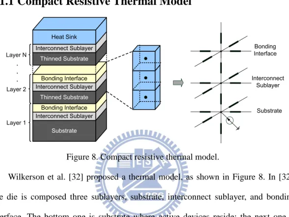
2.1.1 Compact Resistive Thermal Model
Substrate Interconnect Sublayer Bonding Interface Thinned Substrate Interconnect Sublayer Bonding Interface Thinned Substrate Interconnect Sublayer Heat Sink Layer 1 Layer 2 Layer N Bonding Interface Interconnect Sublayer Substrate
Figure 8. Compact resistive thermal model.
Wilkerson et al. [32] proposed a thermal model, as shown in Figure 8. In [32], one die is composed three sublayers, substrate, interconnect sublayer, and bonding interface. The bottom one is substrate where active devices reside; the next one is interconnect sublayer where metal wire and via reside; the last one is bonding interface which attach between two adjacent dies. Heat produced from active device dissipates from substrate to heat sink, and then it is transmitted to the ambient air (25℃).
First, each die is divided into numerous grids, whose size is determined by the smallest module of input. Then each gird is partitioned into several nodes depended on the number of sublayers per die. Nodes connect to adjacent ones with thermal resistance. Thermal resistance determined based on grid size and thermal conductivity as expressed in Equation (1). L represents the length; k represents the thermal conductivity; A represents the cross section area.
10
(1) Next, there is current source depended on power density on the substrate node, and then the 3D stacked die becomes a complicated mesh circuit. Finally, the model applies thermal-electrical duality [33], as shown in Table 2, to create a steady-state temperature profile for the given floorplan. Because of thermal-electrical duality, Equation (2) and (3) are dual.
Table 2. Thermal-electrical duality [33].
Thermal quantity Unit Electrical quantity Unit
T, Temperature difference K V, Voltage difference V P, Power density W I, Current source A Rth, Thermal resistance K/W R, Electrical resistance Ω
(2) (3) This thermal model is accurate but it takes minutes to evaluate once. In floorplan, using thermal model to evaluate temperature of floorplan with one perturbation during simulated annealing. Then there are a great amount of perturbations, so thermal model has to be used as many as number of perturbations. It is too time-consuming, so it is not suitable for floorplan. Some accurate thermal models like finite element method (FEM) [34] and finite difference method (FDM) [35] have long runtime. They are not suitable for application of floorplan, neither.
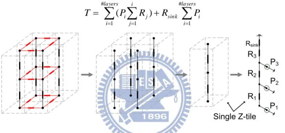
2.1.2 Z-Tile
Floorplan prefers fast thermal model. Cong et al. [29] proposed a simplified compact resistive thermal model. They consider that vertical path is primary heat dissipation path. Thus, for runtime reason, they simplify the compact resistive thermal model by ignoring horizontal thermal resistance, as shown in Figure 9. By only
A k L Rth IR V th PR T
11
considering vertical thermal resistance, the mesh circuit becomes independent thermal resistance pillars. This is why this model is named Z-tile model.
The ability of heat distribution depends on the distance to heat sink. Farther from heat sink, lower heat ability of heat distribution, that is, higher temperature. The maximum temperature will occur at the layer farthest from the heat sink, which is bottom layer. Thus, the formula of Z-tile for temperature evaluation is expressed as Equation (4). In Equation (4) the temperature is superimposed on temperature of upper layer. (4) P1 P2 P3 R1 R2 R3 Rsink Single Z-tile
Figure 9. Construction of Z-tile model.
2.2 Motivation
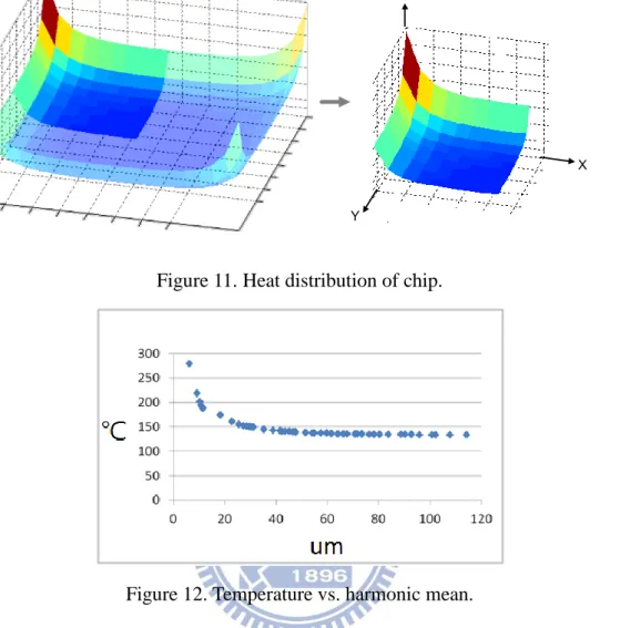
Thermal resistances are determined by Equation (1), and each grid size of Z-tile and thermal conductivity are the same. Therefore, thermal resistances of each Z-tile are the same. In this situation, module placed everywhere at same layer produces same temperature. Actually, Figure 10 shows evaluation of the same module but location in different positions of a chip. The module placed at corner produce higher temperature than it placed at center. This is because the boundaries of chip are adiabatic. However, in Z-tile, module produces same temperature as it is placed at different locations. Z-tile cannot show location-dependent property.
layers i i sink i j j layers i i R R P P T # 1 1 # 1 ) (12
(a) (b)
Figure 10. temperature produced by module placed at (a) corner (b) center. Thus, we conduct an experiment to verify our view of point. Based on compact resistive thermal model, we use single identical current source at different grids with same layer. Then we record the temperature of grid where current source is. Because the chip is symmetrical, temperature distribution is symmetrical, too. So we only have to observe quarter of chip, and the original point is at corner, as shown in Figure 11. In Figure 11, there are 20 × 20 grids with 12um × 12um. We can easily discern that the higher temperature be produced while gird is more close to the boundaries. And we collate the relation between temperature and distance to original point, which locate at (0,0,0), as shown in Figure 12, where y coordinate represents temperature and x coordinate represents harmonic mean (HM), as expressed in Equation (5).
(5) 1 1 1 2 ) , ( y x y x HM
13
X Y
Z
Figure 11. Heat distribution of chip.
Figure 12. Temperature vs. harmonic mean.
Compared to these two thermal models, compact resistive thermal model consider horizontal and vertical heat dissipation, so it can show the location-dependent property. Nevertheless, as we discussed before, the runtime of compact resistive thermal model is too long to be applied for floorplan. On the other hand, by ignoring horizontal thermal resistance, runtime of Z-tile improve a lot. Under this structure, Z-tile only considers vertical heat dissipation; it cannot differentiate the location issue.
Two models both have drawbacks. Compact resistive thermal model has runtime problem; Z-tile cannot show the location-dependent property. Therefore, in this thesis we propose a novel thermal model with location-dependent property and fast execution time for floorplan.
14
2.3 Problem Formulation
Given a set of module information, including height, width, and power density, a netlist, and the number of layers. Out method is to find the location and resided layer of each module to minimize the footprint area, total wirelength, number of TSVs, and peak temperature in floorplan with fix-outline constraint.
15
Chapter 3
Thermal-aware Floorplan
Algorithm
3.1 Proposed Thermal Model
We want a location-dependent thermal model without runtime increase. We will introduce how we build this thermal model in this section.
No matter how accurate the model is, if runtime is too long, then it is not a good model for floorplan. Hence, runtime is first issue needed to be concerned. Thus, we prefer the simple and fast model, so we construct our thermal model based on the Z-tile-based model. As we know, Z-tile cannot show the location-dependent property. It is a location-independent thermal model.
Thermal resistances of each Z-tile are the same, so the temperature module produced are no deference while module is placed everywhere at same layer. If power density doesn’t change, alter thermal resistance such that temperature will change. So we let the central thermal resistance be smaller than peripheral thermal resistance. In this way, modules placed at corner will produce higher temperature than it placed at center.
We want our thermal model can reflect location-dependent property on compact resistive thermal model. Therefore, we let the distribution of thermal resistance on our thermal model display distribution of temperature on compact resistive thermal model. For example, as shown in Figure 13, we want to construct the single Z-tile located at corner. First, we put unit power density as current source at corner with top layer, point a, and after circuit arrives at steady-state condition, temperature of this point is Va. Then the top thermal resistance of Z-tile-based thermal model is Va, because if we
16
put same unit power density as current source at point a, the temperature point a produce is as same as the temperature compact resistive thermal model produce. Then we do same thing at the point located at corner with the second layer from top, point b. The temperature of point b is Vb, and then the point b in Z-tile-based thermal model must to produce the same temperature with unit power density. Thus, the second thermal resistance from top is Vb – Va. If we put unit power density at point b in Z-tile-based thermal model, the temperature will be Vb, [(Vb – Va)+Va] ×1=Vb. And do the same thing until the bottom thermal resistance is determined. Remainder thermal resistances are determined as same way.
Compare to Z-tile, all thermal resistances of Z-tile are the same. In our model, thermal resistances have different values at single Z-tile with different layers, and they will be different as placed at different location with same layer. By altering the thermal resistance, Z-tile-based thermal model can show the location-dependent property and the thermal resistances reflect the temperature distribution of compact resistive thermal model. This new location-dependent thermal model is named location-dependent Z-tile (LDZT).
LDZT has location-dependent property by altering thermal resistances, and it preserves the speed of Z-tile. Because the formulation for temperature evaluation is the same, LDZT has the same runtime as Z-tile. We realize the location-dependent property on Z-tile without runtime increase.
17
a
b
c
a
b
c
Va
Vb – Va
Vc – Vb
Figure 13. Thermal resistance evaluation.
3.2 Proposed Thermal-aware Floorplan
Algorithm
The flow chart of our algorithm is shown in Figure 14 and the cost function is shown in Equation (6). The items in Equation (6) are shown as Equation (7) – (11). We use SP representation to represent the floorplan and HPWL to evaluate the wirelength. TSV cost is TSV count and temperature cost is maximum temperature in LDZT. The last cost, RF, will be introduced in section 3.2.1. After floorplan finish, we use compact resistive thermal model to evaluate the temperature accurately.
18 Floorplan information Perturbation of solution Accept? Stop? Restore floorplan Reduce annealing temperature Floorplan result Heat evalutation SA-based engine N Y N Y
Figure 14. Algorithm flow.
(6) (7) (8) (9) (10) (11) RF LDZT NumTSV HPWL 2 area
1 Cost Cost Cost Cost Cost
Cost 3 4 5 old old new area Footprint Footprint Footprint Cost old old new HPWL HPWL HPWL HPWL Cost old old new NumTSV NumTSV NumTSV NumTSV Cost old old new LDZT maxT(LDZT) maxT(LDZT) maxT(LDZT) Cost old old new RF RF RF RF Cost
19
3.2.1 Repulsion Force
LDZT is applied to our proposed floorplan algorithm. Before LDZT is used in floorplan, we analyze its characteristic. LDZT is a Z-tile-based model, so it has the property of Z-tile, such as let module with high power density be put at upper layer, and its runtime is as fast as Z-tile. Besides, LDZT can show the location-dependent property, this is the most important improvement in Z-tile. As we discussed before, we alter thermal resistances to realize location-dependent property. In LDZT, the module with high power density will be placed near the center, and this tendency will cause potential hotspot. Because LDZT is Z-tile-base model, it also ignores horizontal thermal resistance. Hence, LDZT can’t consider the horizontal heat dissipation, even though it has location-dependent property. The potential hotspot will occur when modules with high power density are all placed near the center. This condition will happen due to the placed tendency of LDZT.
Although the hotspot occurred at center is better than it occurred at corner, we want the temperature distribution is as uniform as possible. Before LDZT is applied to floorplan, we want to solve this problem. We want the modules with high power density are not close to each other, so we add the force to exclude them. Logan et al. [36] proposed a repulsion force (RF) cost in floorplan to exclude the modules with high power density. They proposed a concept of thermal coupling, which means it has hotter temperature when modules with high power density closer to each other. Thus, they define the hot modules whose power density are higher than average power density and then define the repulsion force, as expressed in Equation (12), to let hot modules exclude each other.
(12)
hot module ij j id
p
p
RF
220
In Equation (12), Pi and Pj represent the power density of hot module i and j
respectively, and dij2 is the distance between these two hot modules. If two hot modules with very high power density, the distance between two must be large enough to minimize the total repulsion force cost. We refine the repulsion force cost to suit our floorplan algorithm, as expressed in Equation (13).
(13)
In Equation (13), we refine four points from [36]. First, we consider all modules, because the definition of hot module has drawback. For instance, if average power density is 50, shouldn’t the module with 49 of power density be considered? Therefore, we consider all modules, and evaluating repulsion force cost is not time-consuming, anyway.
Second, we change the addition to multiplication. Because addition cannot precisely determine whether the reciprocal effect of two modules is good or not, we change it. For example, doing addition of two modules with 1 and 99 of power density respectively is 100. And then do it of two modules with 50 and 50 of power density. The answers are the same. So these two sets of modules are the same for repulsion force cost. But, the set of modules with 1 and 99 of power density is much better than the other set, because the thing that one module is hot and the other is cool is good for heat dissipation. In multiplication, the answer is large if and only if two modules both have high power density. This is why we adopt the multiplication.
The next, [36] consider the hot module with all layers to evaluate repulsion force cost. Because we use LDZT to consider vertical heat dissipation already, we don’t have to consider vertical repulsion force. Thus, we calculate repulsion force layer by layer, and then we sum up the repulsion force on each layer.
The last point we refine is adding the different weights to different layers. High
layers k layer module ij j i k1
w
d
p
p
w
RF
k # 1 2 1,
21
repulsion force of one layer means there are many modules with high power density or some modules with high power density are closer to each other. No matter what condition is, high repulsion force of one layer represents there is high probability the layer has hotspot. Thus, we want high repulsion force occur at upper layer, because upper layer is close to heat sink. So, we increase the tolerability of repulsion force at upper layer by the additional weight.
3.2.2 Over-heat Prevention Zone
We use the algorithm introduced previously for 100 random seeds. The worst case of 100 floorpalns is shown in Figure 15. The hotspot occurs at original point, the corner of floorplan. This is not condition we except, because we will place modules with high power density at center by LDZT. So we analyze this condition. There are two reasons causing the hotspot occurs at original point.
Figure 15. Temperature distribution
The first reason is we use SP representation to represent floorplan. We will place modules from bottom-left to top-right by SP representation. Hence, the density of module of original point (bottom-let corner) will be higher than the other corners, as shown in Figure 16.
22
Figure 16. Modules are placed by using SP representation.
The other reason is degree of perturbation. Because there are other items in cost function, all items of cost function determine where the module is placed. Although the thermal cost want to place module away from corner, other items may not want. In brief, other items may restrict the degree of perturbation.
In order to let the hotspot be away from original point, we want the modules with high power density be placed away from original point. We observe the SP representation. In SP representation, if notation A is always left to notation B in two sequences (Γ+, Γ-), the location of module A will be left to the location of module B. Otherwise, if notation A is left to notation B in sequenceΓ+, but it is right to notation B in sequenceΓ-. In this condition, the module A will be placed above the module B. Based on this property of SP representation, the notation get closer to left part of sequences means that the module of this notation get closer to original point (bottom-left).
After observation of SP representation, we consider the N leftmost rooms in two sequences as over-heat prevention zone (OHPZ), and N is the zone size. The purpose of OHPZ is that the modules with high power density cannot be located in OHPZ. Then, we define over-heat module whose power density is higher than average power density plus standard deviation of power density. We constrain that the over-heat module cannot be placed in OHPZ.
23
Chapter 4
Parallel Floorplan Algorithm on
GPGPU
In this chapter, we introduce the way we parallelize the floorplan and how the parallel algorithm can obtain maximum speedup. As listed in section 1.3, using global memory will cause large latency, so we have to use it as less as possible. There are two conditions where we use global memory. One is communication between blocks, and the other is communication between CPU and GPU. For first condition, the best way to prevent is that let blocks not to communicate each other. Thus, we let blocks deal with independent issues. In this way blocks don’t need to communicate each other. The latter condition can’t be avoided. If CPU doesn’t transmit data to GPU, there are no data to use for CUDA kernel function. On the other hand, if GPU doesn’t transmit data to CPU, CPU can’t receive the data which are treated already. Therefore, we can’t avoid this condition. All we can do is reduce the frequency and quantity of data of communication.
There are two types of data sent to GPU from CPU. One is the data which do not change during SA procedure, such as netlist, power density of module, and thermal resistance. The other one will change during SA procedure, such as location of modules, and height/width of modules. In order to reduce the frequency of communication, we send the type one data to GPU once before SA procedure. And during SA procedure, we only send type two data to GPU to reduce the quantity of data of communication.
The items of cost function are area, wirelength, TSV count, temperature, and repulsion force. We consider each item as respective kernel function, because each item evaluation is suit for different number of blocks and threads.
24
We will introduce the method we parallelize these items in turn.
4.1 Parallel Floorplan – Area
SP representation places modules from bottom-left to top-right. When module is placed, its location is relative to the modules which are placed already. Thus, the module is dependent while calculating area.
Because the data are dependent, we can’t divide the algorithm into independent parts completely. We divide the algorithm by breaking the for-loop as shown in Algorithm 1, pseudo-code of area evaluation for Parquet 4.5 [38]. After breaking the for-loop, the pseudo-code is performed be each thread. In this way, the time complexity of area evaluation becomes O(#modules) from O(#modules2).
25
Algorithm 1. The pseudo-code for area evaluation [38]. Area evaluation for( i = 1 to #modules ) match[X[i]].x = i; match[Y[i]].y= i; Length[i] = 0; for( i = 1 to #modules ) b = X[i]; p = match[b].y; Position[b] = Length[p]; t = Position[b] + weights(b); for( j = p to #modules)
if( t > Length[j] ) Length[j] = t; else break;
return Length[#modules];
In this algorithm, the independent elements are x coordinate evaluation, y coordinate evaluation, and different layers. We can evaluate x coordinate and y coordinate of each module and module coordinate at different layers simultaneously. So the number of blocks is 2 × #layers. After the evaluation, we only return the footprint area to CPU to reduce the communication time (quantity of data of communication). The module data, like height/width and coordinate, are stored at global memory, because the shared memory will be clear while the kernel function is end. The module date we store are used for other kernel function. Like wirelength evaluation, we need module coordinate to calculate it. Other kernel function all need module coordinate, so we evaluation area first.
26
4.2 Parallel Floorplan – Wirelength and TSV
Count
We deal with these two items by using the same data, netlist, and module coordinate. In order to reduce the times of communications between shared memory and global memory, we evaluate these two items in one kernel function together.
In this algorithm, the independent element is net. Because the wirelength of net and number of layers the net cross are independent, we can deal with one net by one thread, the time complexity becomes O(maximum #degrees of a net) from O(total #degrees). And we sum up the values of each thread to get the total wirelength/TSV count by tree reduction technique, as shown in Figure 17. By this technique, the time complexity for addition is becomes O(log#nets) from O(#nets).Finally, we only send
total wirelength and TSV count to CPU.
10 15 7 8 10 18 25 25 7 25 50
Figure 17. Tree reduction technique.
4.3 Parallel Floorplan – Temperature
4.3.1 Power Density Evaluation
The way to evaluate temperature is expressed in Equation (3). Before we evaluate temperature, we calculate power density first. The power density of the grid
27
is calculated by summation of power density of each module multiplied by its area ratio, the overlapping area between module and grid divide by grid area, as shown in Equation (14)
(14)
In Equation (14), gi represents grid i, mj represents module j, Li represents the
layer where grid i reside, Pj represents power density of mj, and ARi,j represents the
area ratio of overlapping between gi and mj.
Power density evaluations of each grid are independent. We can evaluate it of different grids simultaneously. One thread deals with one grid, and each grid scans all modules at layer where grid resides to calculate the power density. Hence, the time complexity becomes O(#modules) from O(#grids×#modules). In this algorithm, number of blocks is determined by number of layers, because different layers are independent element. Besides, we only need the module data with one layer on one block, so we can let module data with same layer be located at shared memory for each block.
4.3.2 Temperature Evaluation
After we calculate power density, we calculate the temperature immediately. Each grid evaluates temperature respectively. Then accumulate the temperature layer by layer, so the maximum temperature will occur at bottom layer. We use the tree reduction technique to find maximum temperature. Different from it used by wirelenght/TSV count, the operation tree reduction technique perform is not addition, but comparison. It finds maximum temperature by comparing two temperatures iteratively. So the time complexity becomes O(log#grids) from O(#grids). And we
return the maximum temperature only.
i j L m j i j ip
AR
g
ty
PowerDensi
(
)
,28
4.4 Parallel Floorplan – Repulsion Force
Repulsion force evaluations of each module are independent. We use one thread to calculate the repulsion force of one module. We evaluate repulsion force layer by layer. The modules with different layers are not used. This is similar to power density evaluation, so we deal with them in the same way. The number of blocks is determined by number of layers, due to the usage of shared memory has been discussed previously.
The thing each thread operates is scan all modules at one layer to calculate the repulsion force, so the time complexity is O(#modules) from O(#modules2). Then we sum up the repulsion force by tree reduction technique, so the time complexity is O(log#modules) from O(#modules). Finally, we return the total repulsion force only.
29
Chapter 5 Experiments
5.1 Environmental Setup
Partition Floorplan Temperature evaluation Module information netlist Construct LDZT SA Floorplan result Thermal profileFigure 18. Experiments flow
The largest cases form benchmark GSRC are shown in Table 3. The total flow is shown in Figure 18 and it is introduced as follow. Before floorplan, we construct thermal model, LDZT, first. Then, the initial layers where modules reside is determined by iLap [37]. The flooplanner we use is Parquet 4.5 [38], a 2D floorplanner, and [39] modify it for 3D floorplan. Next, the experimental settings of floorplan are shown as follow. The fix-outline constraints we set are 20% whitespace for 4-layer design and the area ratio is 1. The floorplan algorithm we proposed has been implemented in C++/Linux environment. Last, we use compact resistive thermal model for thermal simulation after floorplan, and the details of it are shown in Table 4.
30 Table 3. Benchmarks. Circuit # of modules # of nets # of pins Max. module Min. module Avg. module Max. net degree Avg. net degree n100 100 885 1873 67 61 22 16 43 43 4 2 n200 200 1585 3599 47 48 12 13 30 30 5 2 n300 300 1893 4358 47 48 12 13 30 30 6 2
Table 4. Physical settings.
Physical Settings Value
Ambient temperature 25℃ Thickness Substrate 30 Interconnect sublayer 150 Bonding interface 10 Thinned substrate 2 Thermal conductivity Substrate 150 Interconnect sublayer 170 Bonding interface 386 Thinned substrate 20
31
5.2 Experimental Results
In this section, we first show the results of floorplan quality, including area, wirelength, TSV count, and temperature. Next we present the runtime analysis in the CUDA platform.
5.2.1 Quality
In this part, we compare our work to related work [29], as shown in following table. Table 5, Table 6, and Table 7 show the results of circuit of n100, n200, n300 respectively. The first row shows the zone size, and the number of bracket means zone size / (#modules/#layers). ZT represents Cong’s work [29] without applying OHPZ technique, which implies the zone size of it is 0. Other columns show the result of varies zone size in LDZT. In the second row, Max_T means the maximum temperature of a single floorplan, and the following columns show the maximum/minimum/average/standard deviation of max_T from floorplans generated by 100 different random seeds. The last, the bottom two rows show the average wirelength and TSV count of 100 floorplans.
The Figure 19, Figure 20, and Figure 21 show the distribution of thermal data of Table 5, Table 6, and Table 7. The top endpoint of line means the maximum of Max_T, and the bottom endpoint of line means the minimum of Max_T. The label on the line means the average of Max_T.
32
Table 5. Experimental results – n100.
Zone size ZT 0(0%) 3(10%) 5(20%) 8(30%) 10(40%) Max_T Std 5.6 5.1 2.8 2.7 2.5 3.0 Max 163.2 160.4 154.6 150.0 151.5 155.3 Min 130.1 133.6 137.2 139.3 135.4 135.1 Avg 148.0 147.0 145.7 144.7 145.0 146.6 WL 131554 131486 130930 131207 131412 131772 TSV 703.2 702.7 699.3 693.4 704.7 701.3
Table 6. Experimental results – n200.
Zone size ZT 0(0%) 5(10%) 10(20%) 15(30%) 20(40%) Max_T Std 2.7 2.2 1.9 1.7 1.4 1.6 Max 193.8 191.4 191.7 192.1 189.4 189.5 Min 181.3 180.7 178.6 179.8 181.2 179.8 Avg 186.3 185.3 184.6 184.4 184.1 184.5 WL 241258 239184 240007 240083 240619 242574 TSV 1540.4 1527.6 1522.7 1520.0 1516.6 1516.8
Table 7. Experimental results – n300.
Zone size ZT 0(0%) 8(10%) 15(20%) 23(30%) 30(40%) Max_T Std 2.5 1.6 1.8 1.3 1.2 1.3 Max 203.7 199.1 197.5 196.2 196.7 197.8 Min 189.3 189.1 187.5 189.2 188.9 189.3 Avg 193.7 193.2 192.8 192.7 193.3 193.5 WL 343863 340112 341874 343885 345545 347358 TSV 1592.5 1570.4 1565.6 1566.8 1564.2 1557.2
33
Figure 20. Thermal data – n200.
Figure 21. Thermal data – n300.
Observing above data, TSV count and wirelength of our work are similar to Cong’s work. Next, observing of the thermal issue. In Figure 19 – Figure 21, the range of the maximum temperatures becomes smaller in our methods. It means our model is stable; in other words, our method is more insensitive to different seeds. If the zone size is too small, over-head modules are still closer to bottom-left corner. But if the zone size is too large, we cannot guarantee the locations of modules in OHPZ are the places we want. Therefore form the results, the range of zone size we recommend is 20% – 30%.
After the analysis of thermal issue, we think that observing maximum temperature of each floorplan is not enough. If there are two floorplans with the same maximum temperature, the temperature distribution of one is cool except the hotspot and the other is hot everywhere. If we only consider maximum temperature, these two floorplans are the same, but the former is better than the latter obviously. So we choose grids in bottom layer with top 5% temperature to analyze. The results are
34
shown in Figure 22 – Figure 24. They show the number of grids with top 5% temperature of Cong’s and our work with 20% zone size. We can see that the number of grids of our work is less than Cong’s in high temperature range. So our work not only has lower maximum temperature but only has more uniform temperature distribution.
Figure 22.Thermal data II – n100.
Figure 23. Thermal data II – n200.
Figure 24. Thermal data II – n300.
5.2.2 Runtime
The following tables and figure show the experimental result of runtime. CPU/GPU, shown in first row, means the floorplan is operated in CPU or GPU. First
35
column shows the elements of cost function, and the follow columns show the runtime/runtime ratio/speedup of these items on CPU/GPU. The rightmost column #Pstr shows the number of streaming processors, this value means ideal upper bound
of speedup. And the Figure 25 show the data of Table 8 – Table 10. Table 8. Runtime – n100.
CPU GPU #Pstr
Ratio(%) Time(s) Time(s) Speedup Ratio(%)
Area 11.4 16.9 0.8 21.1 1.9 256 WL 4.2 6.2 1.3 4.8 3.0 64 Temp 81.1 120.1 2.8 42.9 6.6 128 RF 3.3 4.9 1.5 3.3 3.5 128 Total 100.0 148.1 6.4 23.1 – – Tovh – – 20.8 – 48.8 – Memcpy – – 15.4 – 36.2 – Total – 148.1 42.6 3.5 100.0 – Table 9. Runtime – n200. CPU GPU #Pstr
Ratio(%) Time(s) Time(s) Speedup Ratio(%)
Area 8.5 78.9 4.8 16.4 4.4 256 WL 2.6 23.9 4.5 5.3 4.1 64 Temp 85.3 792.6 18.2 43.5 16.6 128 RF 3.6 33.2 9.0 3.7 8.2 128 Total 100.0 928.6 36.5 25.4 – – Tovh – – 41.8 – 38.1 – Memcpy – – 31.4 – 28.6 – Total – 928.6 109.7 8.5 100.0 –
36
Table 10. Runtime – n300.
CPU GPU #Pstr
Ratio(%) Time(s) Time(s) Speedup Ratio(%)
Area 6.7 190.1 14.4 13.2 6.9 256 WL 1.6 46.1 8.0 5.8 3.8 64 Temp 87.7 2479.6 56.8 43.7 27.3 128 RF 4.0 112.9 27.0 4.2 13.0 128 Total 100.0 2828.7 106.2 26.6 – – Tovh – – 55.3 – 26.5 – Memcpy – – 46.9 – 22.5 – Total – 2828.7 208.4 13.6 100.0 – (a) (b) (c)
Figure 25. (a) Runtime – n100 (b) Runtime – n200 (c) Runtime – n300.
We can see the speedup of GPU and number of streaming processors are different. Because the algorithm is not parallel completely and there are drawbacks we will discuss later on CUDA. First, we discuss the speedup of area. Because we evaluate coordinates module by module then get the final area when all modules are done. That is, data are highly dependent, and each thread may idle for each other until total thread finish their work. Thus, the speedup decrease due to dependent data. Second, when computing wirelength, because there are a great amount of branch
37
instructions on wirelength evaluation, performance may reduce by CUDA property we introduced previously. Next, the difference between speedup and number of streaming processors on temperature evaluation is smaller than it on other evaluations. This is because the temperature evaluation of each grid is independent, which is introduced before. Thus, the temperature evaluation has better parallelism than others. However, the computations done after power density evaluation delay the speed, so the final speedup gets reduced. Last, we analysis the speedup of repulsion force. In general, the number of streaming processors is the maximum speedup. Nevertheless, as we introduce before, the number of divider on each multiprocessor is much fewer than the number of thread on each multiprocessor, and there is division in repulsion force evaluation, so the maximum speedup is determined by the total number of dividers. The total speedup of these evaluation approximate 25. Finally, there are still communication time and kernel overhead, the final speedup reduce due to these drawbacks. The time complexity of communication time and kernel overhead increase linearly with module size, but the time complexity of evaluation increase faster than module size. Hence, while module size becomes larger, the ratio of runtime of these two drawbacks to total runtime becomes smaller. This is why the final speedup becomes larger as larger module size.
38
Chapter 6 Conclusion
In this thesis, we propose a fast location-dependent thermal model, and a thermal-aware floorplan algorithm. And we implement the algorithm on CPU and GPGPU.
LDZT, the fast thermal model we propose, can show the location-dependent property without runtime increase. Moreover, we also propose two strategies to prevent generating hotspots. We refine the repulsion force to exclude the module with high power density. This technique can also compensate the thermal coupling issue due to omitting lateral thermal resistances in LDZT. And we define a zone, named over-heat prevention zone, to prevent left-bottom corner of floorplan getting over-heat during the SA procedure. The over-heat module, whose power density is higher than average power density by standard deviation of power density, cannot be placed in this zone. By these strategies, we can reduce the maximum/average temperature and decrease the number of grid in high temperature range. Additionally, the floorplanner is insensitive to random seeds, which implies the robustness of our method is quite good. Finally, we use CUDA to speed up the runtime. We get 3.5X – 13.6X speedup. The speedup gets significant as the size of the design grows.
39
Reference
[1] “International Technology Roadmap for Semiconductor,” Semiconductor Industry Association 2005–2010.
[2] G. Metze, M. Khbels, N. Goldsman, and B. Jacob, “Heterogeneous integration,” Tech Trend Notes, vol. 12, no. 2, p. 3, 2003.
[3] A. W. Topol, D. C. La Tulipe, L. Shi, D. J. Frank, K. Bernstein, S. E. Steen, A. Kumar, G. U. Singco, A. M. Young, K. W. Guarini, and M. Ieong, “Three-dimensional integrated circuits,” IBM J. of Research and Development, vol. 50, no. 4.5, pp. 491–506, Jul. 2006.
[4] K. Banerjee, S. J. Souri, P. Kapur, and K. C. Saraswat, “3-D ICs: a novel chip design for improving deep submicron interconnect performance and systems-on-chip integration,” Proc. IEEE, vol. 89, no. 5, pp. 602–633, May 2001.
[5] R. Tummala and V. Madisetti, “System on chip or system on package?” IEEE Design & Test of Computers, vol. 16, no. 2, pp. 48–56, Apr.–Jun. 1999.
[6] P. H. Shiu and K. S. Lim, “Multi-layer floorplanning for reliable system-on-package,” Proc.Int’l Symp. Circuits and System, pp. 23–26, 2004. [7] S. Spiesshoefer, Z. Rahman, G. Vangara, S. Polamreddy, S. Burkett, and L.
Schaper, “Process integration for through-silicon vias,” J. of Vacuum Science and Technology A, vol. 23, no. 4, pp. 824–829, Jul. 2005.
[8] SOCcentral. [Online]. Available: http://www.soccentral.com
[9] S. Das, A. P. Chandrakasan, and R. Reif, “Calibration of rent's rule models for three-dimensional integrated circuits,” IEEE Trans. Very Large Scale Integration Systems, vol. 12, no. 4, pp. 359–366, Apr. 2004.
[10] A. Rahman and R. Reif, “System-level performance evaluation of three-dimensional integrated circuits,” IEEE Trans. Very Large Scale Integration Systems, vol.8, no.6, pp. 671–678, Dec. 2000.
[11] S. Das, A. Fan, K. Chen, C. S. Tan, N. Checka, and R. Reif, “Technology, performance, and computer-aided design of three-dimensional integrated circuits,” Proc. Int’l Symp. Physical Design, pp. 108–115, 2004.
[12] I. Kaya, S. Salewski, M. Olbrich, and E. Barke, “Wirelength reduction using 3D physical design,” Int’l Workshop Integrated Circuit System Design, pp. 453–462, 2004.
[13] I. Loi, S. Mitra, T. H. Lee, S. Fujita, and L. Benini, “A low-overhead fault tolerance scheme for TSV-based 3D network on chip links,” Proc. Int’l Conf. Computer-Aided Design, pp. 598–602, 2008.
40
[14] W. R. Davis, J. Wilson, S. Mick, J. Xu, H. Hua, C. Mineo, A.M. Sule, M. Steer, and P. D. Franzon, “Demystifying 3D ICs: the pros and cons of going vertical,” IEEE Design & Test of Computers, vol. 22, no. 6, pp. 498–510, Nov.–Dec. 2005. [15] D. F. Wong and C. L. Liu, “A new algorithm for floorplan design,” Proc. Design
Automation Conf., pp.101–107, 1986.
[16] R. Otten, “Automatic floorplan design,” Proc. Design Automation Conf., pp.261–267, 1982.
[17] Y.-C. Chang, Y.-W. Chang, G.-M.Wu, and S.-W.Wu, “B*-trees: A new representation for nonslicing floorplans,” Proc. Design Automation Conf., pp. 458–463, 2000.
[18] H. Murata, K. Fujiyoshi, S. Nakatake, and Y. Kajitani, “VLSI module placement based on rectangle-packing by the sequence pair”. IEEE Trans. Computer Aided Design of Integrated Circuits and Systems, vol. 15, no. 12, pp. 1518–1524, Dec. 1996.
[19] P.-N. Guo, C.-K. Cheng, and T. Yoshimura, “An O-tree representation of nonslicing floorplan and its applications,” Proc. Design Automation Conf., pp.
268–273, 1999.
[20] Z. Li, X. Hong, Q. Zhou, Y. Cai, J. Bian, H. H. Yang, V. Pitchumani, and C.-K Cheng, “Hierarchical 3D floorplanning algorithm for wirelength optimization,” IEEE Trans. Circuits and Syst.I: Regular Papers, vol. 53, no. 12, pp. 2637–2646, Dec. 2006.
[21] T. Yan, Q. Dong, Y. Takashima, Y. Kajitani, “How dose partitioning matter for 3D floorplanning,” Proc. ACM Great Lakes symposium on VLSI, pp. 73–78, 2006.
[22] Z. Li, X. Hong, Q. Zhou, S. Zeng, J. Bian, W. Yu, H. H. Yang, V. Pitchumani, and C.-K. Cheng, “Efficient thermal via planning approach and its application in 3-D floorplanning,” IEEE Trans. Comput.-Aided Design Integr. Circuits Syst., vol. 26, no. 4, pp. 645–658, Apr. 2007.
[23] Z. Li, X-L. Hong, Q. Zhou, S. Zeng, H. Yang, V. Pitchumani, and C-K. Cheng, “Integrating dynamic thermal via planning with 3D floorplanning algorithm,” Proc. Int’l Symp. Physical Design, pp. 178–185, 2006.
[24] Y. Huang, Q. Zhou, and Y. Cai, “Thermal via planning aware force-directed floorplanning for 3D ICs,” Int’l Conf. Application-Specific Integrated Circuit, pp. 751–753, 2009.
[25] E. Wong and S. Lim, “Whitespace redistribution for thermal via insertion in 3D stacked ICs,” Proc. Int’l Conf. Computer Design, pp. 267–272, 2007.
41
[26] X. Li, Y. Ma, X. Hong, S. Dong, and J. Cong, “LP based white space redistribution for thermal via planning and performance optimization in 3D ICs,” Proc. Asia and South Pacific Design Automation Conf., pp. 209–212, 2008. [27] Y. Chen, H. Zhou, R. Dick, “Integrated circuit white space redistribution for
temperature optimization,” Proc. Int’l Conf. Design, Automation & Test in Europe, pp. 1–6, 2011.
[28] L. Xiao, S. Sinha, J. Xu, E. Young, “Fixed-outline thermal-aware 3D floorplanning,” Proc. Int’l Conf. Design Automation Conference, pp. 561–567, 2010.
[29] J. Cong, J. Wei, and Y. Zhang, “A thermal-driven floorplanning algorithm for 3D ICs,” Proc. Int’l Conf. Computer-Aided Design, pp. 306–313, 2004.
[30] J. Kung, I. Han, S. Sapatnekar, and Y. Shin, “Thermal singature: a simple yet accuate thermal index for floorplan optimization,” Proc. Int’l Conf. Design Automation Conference, pp. 108–113, 2011.
[31] http://www.nvidia.com/object/cuda_home_new.html
[32] P. Wilkerson, A. Raman, and M. Turowski, “Fast, automated thermal simulation of three-dimensional integrated circuits,” Int’l Society Conf. on Thermal Phenomena, vol. 1, pp. 706–713, Jun. 2004.
[33] W. Huang, “HotSpot - A chip and package compact thermal modeling methodology for VLSI design,” PhD Thesis, ECE, University of Virginia, 2007. [34] W. K. Chu and W. H. Kao, “A three-dimensional transient electro thermal
simulation system for IC’s,” Proc. Therminic Workshop, pp. 201–207, 1995. [35] T.-Y. Wang, Y.-M. Lee, and C. C.-P. Chen, “3D thermal-ADI: an efficient
chip-level transient thermal simulator,” Proc. International Symposium Physical Design, pp. 10–17, 2003.
[36] S. Logan, M. Guthaus, “Fast thermal-aware floorplanning using white-space optimization,” Proc. Int’l Conf. Very Large Scale Integration, pp. 65–70, 2009 [37] Y-S. Huang, Y.-H. Liu, and J.-D. Huang, “Layer-aware design partitioning for
vertical interconnect minimization,” Proc. IEEE Computer Society Annual Symp. on VLSI, pp. 144–149, 2011.
[38] S. N. Adya and I. L. Markov, “Fixed-outline floorplanning: enabling hierarchical design,” IEEE Trans. Very Large Scale Integr. (VLSI) Syst., vol. 11, no. 6, pp. 1120–1135, Dec. 2003.
[39] C-Y. Huang, “Efficient TSV planning via congestion-aware block shifting in 3D floorplanning,” Master Thesis, EE, National Chiao Tung University, 2012.
![Figure 1. Relative delay vs. feature size [1].](https://thumb-ap.123doks.com/thumbv2/9libinfo/8471740.183566/10.892.242.641.532.852/figure-relative-delay-vs-feature-size.webp)
![Figure 3. Wire bonding technology [8].](https://thumb-ap.123doks.com/thumbv2/9libinfo/8471740.183566/11.892.134.765.514.972/figure-wire-bonding-technology.webp)
![Table 2. Thermal-electrical duality [33].](https://thumb-ap.123doks.com/thumbv2/9libinfo/8471740.183566/19.892.128.759.382.707/table-thermal-electrical-duality.webp)