Microfabrication Using
Silicon Mold
Inserts
and Hot
Embossing
Liwei L i d ) , Chun-Jung Chiu'), Walter Bache?)
and
Mathias Heckele2)
')Institute of Applied Mechanics, National Taiwan University, Taipei, 106, Taiwan, R.O.C. 2)Forschungszentrum Karlsruhe, Institut for Mikrostrukturtechnik, 76021 Karlsruhe, GermanyAbstruct- We have successfully demonstrated the feasibility of fabricating three-dimensional mi- crostructures by using a combined silicon mold in- sert and micro hot embossing process (SMIHE). Anisotropic silicon wet etching process has been used to define microstructures on top of a four inch silicon wafer. The whole wafer is then used as the mold insert in a micro hot pressing machine to duplicate plastic microstructures repeatedly. Fine micro pyramid shape microstructures with base width of 30 pm and height of about 21 pm have been fabricated by this method as a demonstra- tion. They have very smooth surfaces and may be suitable for optical applications. This new pro- cess shows promise for achieving high yield, reli- able fine micro structures on plastic films.
I. INTRODUCTION
The modern microfabrication process started when the in- tegrated circuit (IC) technology was first introduced in the early 1960s. Batch fabrication is the key factor for the suc- cess of IC process. Nowadays, IC devices have been batch fabricated and sold with prices that other technologies can not compete with. Mechanical engineers, on the other hand, have developed technologies like injection molding and hot embossing process to duplicate plastic structures which have been used in our daily life, from drinking cups to frames of computers. Both of the IC technology and in- jection molding or hot embossing processes have a similar function - to reproduce products quickly and massively. Recent development of MEMS (Micro Electro Mechani- cal Systems) has basically followed the success of IC tech- nology and injection molding/hot embossing processes. Silicon micromachining uses silicon as a mechanical ma- terial [l] and IC compatible processes have been used or modified to make fine microstructures for applications in different areas. LIGA process [2], which uses X-ray lithog- raphy, electroplating and molding process to fabricate mi- crostructures is one of the applications among many oth- ers to use injection molding or hot embossing process for
fabricating micro parts. One of the possibility is to use sil- icon micromachining process and combine it with molding process to fabricate microstructures.
Previously, diamond precision machining has been used for making micro cars [3], micro channels or micro pyra- mids
[4].
However, it is difficult to maintain the surface roughness of microstructures made by these mechanical machining methods.A
DEEM0 (Dry Etching, Electro- plating and Moulding) process which uses dry silicon etching process, electroplating process and moulding pro- cess to make deep three-dimensional structures has also been developed [5]. In this paper, anisotropic silicon etch- ing process is used to make fine microstructures on silicon wafer which is then used as mould inserts in the hot em- bossing process to make plastic microstructures. In case of isotropic silicon etching, this combination has recently been applied for the fabrication of microlenses [6, 71.11. DESIGN AND FABRICATION
A. The SMIHE Process
The SMIHE (Silicon Mold Insert Hot Embossing) process consists of two major steps: the silicon mold insert and hot embossing as shown in the left hand side and right hand side of Fig. 1, respectively. First, silicon wafer is gone through the lithography process by using the stan- dard UV light exposure as seen in Fig. 1 (a). The patterns on the mask are then transferred onto the photoresit on top of the silicon wafer. Silicon micromachining process is then followed by either dry etching or wet etching pro- cesses to make three-dimensional microstructures into the silicon wafer. Fig. l(b) applies after these steps. The masking material is then removed and the wafer has pat- terned microstructures on top now as shown in Fig. l(c). The whole silicon wafer is then used as the mold insert in a hot embossing machine m illustrated in Fig. l(d). Plastic material which generally has transition point at rnedium temperature is then used for the hot embossing process. The fine micro patterns are transferred onto the plastic material and this hot embossing process can be re-
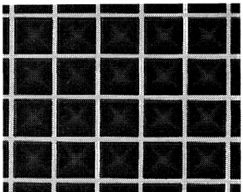
Figure 3: An optical photo showing a portion of silicon mold insert.
small bubbles and incompletely filled pyramid tips. Step- wise increasing temperature and force up to 2 O O O C and 10 k N yields better results. Finally we realized nearly perfect micropyramids by varying also the molding time under optimum temperature and pressure conditions. The high molding forces we introduced arose a new problem in the demolding process : for small forces demolding takes place automatically upon cooling to room temperature. In the case of high molding force, this was no longer sufficient. We had to apply temperatures around O°C and introduce a water film between mold and polymer making use of the additional capillary forces exerted in this way. With a small number of tests, we achieved a parameter definition which was sufficient for the experiments described here. On the other hand, fine tuning of the process conditions will be necessary to obtain perfect molding results.
Figure 4: A SEM microphoto showing the silicon mold insert with defects.
111. FABRICATION RESULTS AND DISCUSSIONS
Showing in Figure 3 is an optical micrograph with pyramid structures made on the surface of a silicon wafer. This micro photo is focused on top of the silicon wafer and pyramid shapes inside the silicon can be barely observed. The size of these pyramids is 30 p m on each side and about 21 pm in height into the silicon. The correspondent angle at the top of the pyramid is about 70" due to the silicon anisotropic etching process. The space from one pyramid to another is about 2 pm, although better width control can be achieved if the lithography step can be improved. Figure 4 is a SEM microphoto showing a portion of the silicon mold insert. On this particular portion, there are defects due to improper lithography and the later sil-
Figure 5: Reflected microstructure made of PMMA ma- terial by the SMIHE process.
(b) ytsk etchGg (d) Hot embossing
Figure 1: The schematic diagram of the SMIHE process.
peated to duplicate fine plastic microstructures as shown in Fig. l(e).
B. Silicon Mold Inserts (SMI)
The silicon mold insert described here was designed and manufactured in the laboratory of Insititute of Applied Mechanics, National Taiwan University, Taiwan. In our try out process, only one mask has been used to make 3-dimensional microstructures on top of silicon wafers for mold inserts. Anisotropic silicon etching technique [8] is used to make these microstructures including V-groove microchannels and micro pyramid structures. The mini- mum width used in the mask is 2pm and the whole four- inch wafer is divided into several areas with size of one centimeter square. Each area has same pyramid arrays with base width of either 100 pm or 30 pm.
Figure 2 shows cross sectional view at the conclusion of key process steps. In the first step of the process, a (100)- oriented lightly doped silicon wafer is put on a masking layer which is thermally grown Si02 as shown in Fig. 2(b). The single mask is then used to define the pattern by using a 1 pm thick resist. The unwanted silicon dioxide layer is then removed by using HF solution as seen in Fig. 2(c). The wafer is then put into 8OoC KOH liquid for anisotropically etching silicon until the pyramids are formed into the silicon wafer. After these steps, Fig. 2(d) applies. The final step is to use HF solution to remove all the S i 0 2 layer and the final structure is shown in Fig. 2(e).
Si02
I
Si SubstrateI
(e)
Figure 2: The process sequences for the silicon mold in- sert.
C. Hot Embossing (HE)
The silicon mold described previously has been used for hot embossing experiments which were performed to- gether with and within the plastic molding group of the institute for Microstructure Technology of the Research Center Karlsruhe, Germany. The mold insert with pyra- mid microstructures to be duplicated has been mounted into a hot embossing machine which is normally used for molding LIGA-microstructures. We applied a 300 pm thick PMMA sheet which was placed on top of the sili- con mold. Hot embossing takes place under vacuum (jO.l mbar) to realize complete filling of the mold with PMMA. After evacuation the mold is heated up to the molding temperature which lies above the glass transition temper- ature of the polymer. Higher temperatures are favourable because the lower viscosity of the PMMA facilitates the molding process. After molding, the polymer is cooled down to below the glass transition temperature. Mold- ing force will be maintained during cooling in order to preserve the PMMA microstructures from shrinking. As soon as the predetermined temperature has been reached, the microstructures can be demolded from the mold in- sert. For every mold insert with different microstructures, the adequate hot embossing parameters like force, temper- ature and time have to be determined. To avoid thermal and mechanical damage of the sensible silicon mold, we started at low temperature and minimal forces. Obser- vation of the result under an optical microscope revealed
icon wet etching process. We have taken microphotos of this area on both the silicon mold insert and the hot embossed PMMA structure intentionally to examine the SMIHE process. Shown in Fig. 5 is the SEM microphoto of' the PMMA microstructure fabricated by the SMIHE pro- cess. Figure 5 looks like the reflected image of Fig.
4
and these two figures demonstrate the excellent reproduction capability of our process. Several individual pyramids on both the silicon mold and the PMMA final product have been examined as marked 1 to 5 in both figures. This examination has further shown exact one to one match between the silicon mold and the plastic products.The oblique view of an SEM micrograph shown in Fig. 6 is the array of plastic micro pyramid structures made by the SMIHE process. The quality and repeatability of
in a SEM micrograph. The small white bar on the right hand side corner represents the scale of only 5 pm. It is clearly observed in this photo that the surfaces of these micro pyramids are extremely smooth and no defects can be identified. The excellent quality of the surface is im- portant for optical applications and this fine result comes from both the fabrication of the silicon mold insert and the hot embossing process. Despite the optimization of the hot embossing process with respect to temperature, force and molding time, in some cases, minor problems oc- curred during demolding, as can be seen from the slightly deformed pyramid tips in Fig. 8. The pyramid tip is com- pletely filled with PMMA, but deformation can be recog- nized in the tip region. Deformation may also be in the origin of the particle which can be seen on the left pyra- mids face (cf. Fig. 8). This particle of only 1 pm thickness
Figure 7: A close view of a micro pyramid. demonstrated the very good quality which are character-
istic for the surfaces of the mold as well as of the PMMA microstructure.
Shown in Fig. 9 is a whole silicon mold inserts (right hand side) and a hot embossed plastic duplicate (left hand side), respectively. The silicon wafer has size of four inches in diameter and the plastic duplicate is a little smaller than four inches due to the limitation of our lithog- raphy machine. This photo demonstrates the feasibility of making large area hot embossing process to increase the production speed.
IV. CONCLUSIONS
The SMIHE (Silicon Mold Insert Hot Embossing) pro- cess has been established in cooperation between IAM, National Taiwan University and IMT, Forschungszentrum Karlsruhe, Germany, and the capability of using a whole four-inch wafer as the mold insert has been successfully
Figure 8: A close view SEM microphoto showing the tip
Figure 9:
A
whole four-inch silicon mold insert (right) and fabricated PMMA microstructure (left).demonstrated. In our first try out process, micro pyramids with base width of 30 pm, height of 21 pm have been fabri- cated. The pyramids are the reflected images of the silicon mold insert which is made by using an anisotropic silicon etching process. No material shrinkage is found during the hot embossing process and the tips of the pyramids remain the original wet etching angle of 70 degrees. The surfaces of the plastic products are very smooth and may be suitable for optical applications.
V . ACKNOWLEDGEMENT
The authors would like to thank Mr. H. Biedermann for assisting in the micro hot embossing process, and Mr. Schiiler for taking all the SEM microphotos, This work was supported by the Mechanical Industry Research Lab- oratories
,
Indus trial Technology and Research Institute (ITRI),
Hsin-Chu, Taiwan. The hot embossing experi- ments in Karlsruhe, Germanyhas
been supported by a cooperation program between National Science Council, Taiwan and DFG, Germany as well as by a memorandum of understanding between National Science Council, Tai- wan and Forschungszentrum Karlsruhe, Germany.REFERENCES
[l] K.E. Peterson. Silicon as a mechanical material. Proc. of the IEEE, 70:420-457, May 1982.
[3] T. Higuchi and Y. Yamagata. Micro machining by ma- chine tools. Proceedings of IEEE Electro Mechanical Systems (MEMS93), pages 1-6, 1993.
[4]
K. Schubert,W.
Bier,G.
Linder, and D. Seidel. Pro- filed microdiamonds for producing microstructures. Industrial Diamond Review, 50:235-239, 1990. [5] J. Elders, H.V. Jansen, and M. Elwenspoek. Deemo:A new technology for the fabrication of microstruc- tures. Proceedings of IEEE Electro Mechanical Sys- tems (MEMS95), pages 238-243, 1995.
[6] U. Kohler, A.E. Guber, W. Bier, and W. Heckele. Fab- rication of microlenses by plasmaless isotropic etching combined with plastic moulding. Sensors and Actua- tors, A53:361-363, 1996.
[7] U. Kohler,
A.E.
Guber, W. Bier,W.
Heckele, and Th. Schaller.
Fabrication of microlenses by plasmaless by combining silicon technology, mechanical microma- chining and plastic molding. Proc. Miniaturized Sys- tems with Macro-Optics and Micromechanics, SPIE,[8] B. Bassous. Fabrication of novel three-dimensional mi- crostructures by the anisotropic etching of (100) and (110) silicon. IEEE Trans. on Electron Devices,
ED-
2687:18-22, 1996.
25:1178-1185, 1978.
[2] W. Bacher, W. Menz, and J. Mohr. The liga tech- nique and its potential for microsystems- a survey.
IEEE Transactions on Industrial Electronics, 42:431- 441, 1995.