Modeling white light-emitting diodes with phosphor layers
Dun-Yen Kang
Institute of Applied Mechanics, National Taiwan University, Taipei, Taiwan Enboa Wua兲
Hong Kong Applied Science and Technology Research Institute, Hong Kong, China Da-Ming Wang
Department of Chemical Engineering, National Taiwan University, Taipei, Taiwan
共Received 21 July 2006; accepted 23 October 2006; published online 4 December 2006兲
With a blue light-emitting diode and a phosphor layer to downconvert blue light to a second light, such as yellow, white light can be produced. The authors developed a one-dimensional model to describe the light propagating in the phosphor layer in terms of light absorption, conversion, and reflection. The parameters required for the model were determined from the data obtained by using multiple-layer phosphor films. The model predicts that, with a reflector between the diode and the phosphor layer that is blue-light transparent but reflects other visible light, the normalized white light intensity is above 0.9, higher than that of conventional packages共0.6–0.8兲. © 2006 American
Institute of Physics. 关DOI:10.1063/1.2400111兴
Blue light-emitting diodes共LEDs兲 have been used as an excitation source for downconverting luminescent material, such as phosphor.1,2Mixing blue light with a downconverted light, such as yellow, white light can be produced. Unfortu-nately a portion of energy would be lost during the mixing processes in conventional packages. Reasons for such energy loss include chip absorption of backward light emitted from phosphor.3A remote-phosphor-package shown in Fig.1 was first proposed in 1999 and such concepts have potential to reduce energy losses.4 This work proposed a one-dimensional model to describe the light absorption, conver-sion, and reflection in LED-phosphor packages.
Shown in Fig.2共a兲is a small cross section of the phos-phor layer with thickness ⌬z. The energy of the blue light emitted from the LED chip is lost during its propagating in the phosphor layer. The lost amount is proportional to the intensity of input blue light 共Lambert-Beer’s law5兲. Part of the energy loss of blue light is caused by its conversion to yellow. The converted light can propagate in the z direction or in the opposite direction.3 The energy of the converted yellow light also dissipates during its propagation within the phosphor layer, following the Lambert-Beer’s law.5In Fig.2, PB represents the intensity of blue light, PY the intensity of yellow in the z direction, and PY−that of yellow light in the
opposite direction. By performing the energy balance, the following three equations were derived:
兩PB兩z+⌬z−兩PB兩z= −␣B⫻ ⌬z ⫻兩PB兩z, 共1兲 兩PY兩z+⌬z−兩PY兩z= −␣Y⫻ ⌬z ⫻兩PY兩z+ 1 2⫻ ⌬z ⫻兩PB兩z, 共2兲 兩PY−兩 z−兩PY−兩z+⌬z= −␣Y⫻ ⌬z ⫻兩PY−兩z+⌬z+ 1 2⫻ ⌬z ⫻兩PB兩z+⌬z, 共3兲
where␣Band␣Yare parameters describing the fractions of
the energy loss of blue and yellow lights during their propa-gations in the phosphor layer,5 respectively, and  is the conversion coefficient for blue light converting to yellow. ␣B, ␣Y, and are properties of the phosphor layer and
de-pendent on the volume fraction of the phosphor particles in the layer,v. With⌬z approaching zero, Eqs.共1兲–共3兲become
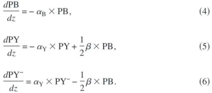
dPB dz = −␣B⫻ PB, 共4兲 dPY dz = −␣Y⫻ PY + 1 2⫻ PB, 共5兲 dPY− dz =␣Y⫻ PY −−1 2⫻ PB. 共6兲
Figure 2共b兲 is a schematic illustration of a flip-chip structure of an LED chip with a phosphor layer thickness h. The intensity of blue light共PB兲 at z=0 is the light intensity from the blue LED, represented by PB0. PY−, the yellow
light intensity traveling in the negative z direction, equals to zero at z = h. By assuming that there is no energy loss in the sapphire substrate, it is obtained that the yellow light inten-sity from the phosphor layer to the active layer is PY−at z = 0, denoted by PY−共0兲. Part of the yellow light reaching the
a兲Electronic mail: [email protected] FIG. 1. Remote-phosphor package proposed by Chen共Ref.4兲.
APPLIED PHYSICS LETTERS 89, 231102共2006兲
0003-6951/2006/89共23兲/231102/3/$23.00 89, 231102-1 © 2006 American Institute of Physics
phosphor layer’s bottom boundary is reflected back to the phosphor layer, with a yellow light reflection coefficient␥. Thus, the following boundary condition can be obtained 共PY共z=0兲=␥PY−共0兲兲. By further assuming that␣B,␣Y, and
are all constant, the solutions to Eqs. 共4兲–共6兲can then be obtained, and the PB, PY, and PY− at z = h are expressed as
PB = PB0⫻ e−␣Bh, 共7兲 PY =1 2 ⫻ PB0 ␣Y−␣B 关e−␣Bh − e−␣Yh兴 +1 2 ␥⫻⫻ PB0 ␣Y+␣B 关e−␣Bh − e−␣Bh−2␣Yh兴, 共8兲 PY−=1 2 ⫻ PB0 ␣Y+␣B 关e−␣Bh− e−␣Bh−2␣Yh兴. 共9兲 In experiment, the PB and PY were measured at different phosphor layer thicknesses h. First we coated on a blue LED chip with a well-dispersed PMMA/phosphor powders/ acetone solution. By the solvent evaporation method,6 a 30m phosphor film was formed on the chip, and the blue and yellow light intensityies, PB and PY, were measured by an integrating sphere. A second 30m film was then coated on the top of the first layer and the light intensity for the chip with 60m film was measured again. We repeated five times the coating and measurement process with a constant v. Having a set of PB and PY data for different thicknesses h, the parameters ␣B,␣Y,, and ␥ were determined by curve fitting with Eqs.共7兲 and共8兲. Varying v and we performed the above experiments and data fitting for eachv. Since the maximum phosphor thickness of our experiments is 150m, much smaller than the chip size, 1 mm, the one-dimensional approximation should still be valid. By experiment the pa-rameters ␣B, ␣Y, , and ␥ under different v values were obtained.
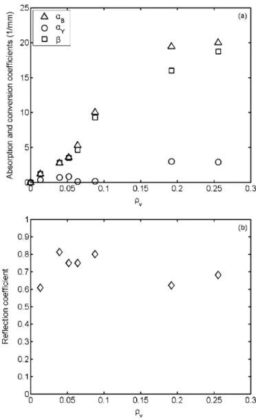
The relationship between the parameters and v is de-picted in Fig. 3. A trend can be observed that with more phosphor in the film, the film would lose more blue and yellow lights and also downconvert more blue light to yellow light. On the other hand, the reflection coefficient ranges between 0.6 and 0.8 and is independent ofv, which is rea-sonable since␥ is a property of the phosphor layer’s bound-ary only. We used linear equations to describe the depen-dence of␣B,␣Y, andonv. Substituting them into Eqs.共7兲
and共8兲, PB and PY can be calculated for a given␥at differ-ent film thicknesses. The calculated results for ␥= 0.7 and experimental data are presented in Fig.4.
According to Eqs.共7兲 and共8兲, the blue and yellow light emitted from a diode with a phosphor layer are functions of ␣B,␣Y,,␥, and h. Since␣B,␣Y, andare functions ofv only, the model parameters can be reduced to v, h, and ␥. Figure4shows the dependence of the normalized total light intensity共共PB+PY兲/PB0兲, the same definition as the extrac-tion efficiency, on v and h. By replotting the normalized intensity versus yellow light fraction 共PY/共PB+PY兲兲, the calculated results shown in Fig.4collapse into a single curve in Fig. 5. The results in Fig. 5 show that, for a specific yellow light fraction, the normalized total light intensity in-creases with increasing reflection coefficient. With ␥= 1.0, the normalized total intensity is above 0.9.
In practical application, for a one-dimensional package geometry, as described in Fig. 2, an increase in ␥ without affecting the blue light emission can be accomplished by placing a yellow light reflector,8 transparent to blue light, between the phosphor film and the LED chip. For complicate
FIG. 2. 共a兲 Schematic plot for a small section of phosphor layer 共one-dimensional model兲 and 共b兲 illustration of the boundary condition at z=0. A portion of backward yellow light, PY−, is reflected by active layer back to
the phosphor layer.
FIG. 3. 共a兲 Dependence of absorption and conversion coefficients on the volume fraction of phosphor in the film and共b兲 relationship between the reflection coefficient and the volume fraction of phosphor in the film. The absorption coefficient is zero whenvequals to zero because the absorption
coefficient of PMMA is effectively zero compared to phosphor particles 共Ref.7兲.
231102-2 Kang, Wu, and Wang Appl. Phys. Lett. 89, 231102共2006兲
package geometry, the design of the package geometry and the reflectivity of the package material would also contribute to the value of␥in our model. When the package surface has higher reflectivity than the chip surface, the remote-phosphor package should have higher␥than the conventional one cause the area involved in reflection is higher, which is be-lieved to be the reason why it has higher light extraction. Details about how to estimate ␥ for complicated package geometry will be published in a subsequent paper.
In summary, with the model presented in this letter, we can predict the blue and yellow light intensities for a LED-phosphor package, as long as the LED-phosphor layer’s thickness, phosphor particle characteristic parameters, ␣B, ␣Y, and ,
and the boundary’s yellow light reflectivity are known. We suggest that higher light intensity can be achieved with any
method to improve boundary reflectivity for yellow light.
1S. Nakamura, Proc. SPIE 3002, 26共1997兲.
2P. Schlotter, R. Schmidt, and J. Schneider, Appl. Phys. A: Mater. Sci.
Process. 64, 417共1997兲.
3N. Narendran, Y. Gu, J. P. Fryssinier-Nova, and Y. Zhu, Phys. Status Solidi
A 202, R60共2005兲.
4H. Chen, U.S. Patent 5,962,971共1999兲.
5F. P. Incropera and D. P. DeWitt, Fundamentals of Heat and Mass
Trans-fer, 5th ed.共Wiley, New York, 2002兲, Chap. 13, pp. 821–822.
6M. Mulder, Basic Principles of Membrane Technology共Kluwer, Dordecht,
1990兲, Chap. 3, p. 59.
7B. Crist, M. E. Marhic, G. Raviv, and M. Epstein, J. Appl. Phys. 51
共1980兲.
8H. A. Macleod, Thin-Film Optical Filter, 3rd ed.共Institute of Physics,
University of Reading, Berkshire, 2001兲, Chaps. 5 and 7, pp. 179–208 and 257–293.
FIG. 4. Relationship between the normalized total intensity 共共PB + PY兲/PB0兲 and the volume fraction of phosphor in film 共v兲—comparison
between calculated results共given␥= 0.7兲 and experiment data.
FIG. 5. Model calculated results to depict effects of reflection coefficient␥ at any given phosphor-layer thickness by plotting normalized total intensity vs yellow light fraction, PY/共PB+PY兲.
231102-3 Kang, Wu, and Wang Appl. Phys. Lett. 89, 231102共2006兲