Low re
flection and photo-sensitive organic light-emitting device with perylene
diimide and double-metal structure
Tien-Lung Chiu
a, Kai-Hsiang Chuang
a, Chi-Feng Lin
a, Yu-Hsuan Ho
a, Jiun-Haw Lee
a,⁎
, Chun-Chieh Chao
b,
Man-Kit Leung
b, De-Hui Wan
c, Cheng-Yu Li
c, Hsuen-Li Chen
ca
Graduate Institute of Photonics and Optoelectronics and Department of Electrical Engineering, National Taiwan University, Taipei 10617, Taiwan, Republic of China
b
Department of Chemistry and Institute of Polymer Science and Engineering, National Taiwan University, Taipei 10617, Taiwan, Republic of China
c
Department of Materials Science & Engineering, National Taiwan University, Taipei 10617, Taiwan, Republic of China
a b s t r a c t
a r t i c l e i n f o
Article history:Received 9 May 2008
Received in revised form 7 December 2008 Accepted 10 December 2008
Available online xxxx Keywords:
Organic light-emitting device Absorption
Destructive interference Photosensitivity
In this paper, an organic light-emitting device (OLED) with low reflection for the entire visible range and at different viewing angles by using an absorptive and photo-sensitive material, N,N'-Bis(2,6-diisopropylphe-nyl)-1,7-bis(4-methoxyphenyl)perylene-3,4,9,10-tetracarboxydiimide (MPPDI), as a black layer (BL) structure was demonstrated. A semitransparent double-metal structure, Al/Ag, was used to reduce the driving voltage and enhance the destructive interference of the BL structure. Combined with the broad absorption band of the MPPDI, the reflectance of such a device shows a 12-times decrease compared to the conventional OLED. Also, a photocurrent enhancement effect was observed in our BL-OLED due to the photosensitive quality of the MPPDI.
© 2009 Elsevier B.V. All rights reserved.
1. Introduction
It is advantageous to use organic light-emitting device (OLED) due to its light weight, self emission, wide view-angle, high luminance efficiency, low drive voltage, and fast response time, all of which make OLED one of the most promising display technologies for the next generation [1,2]. However, ambient reflection from the metal elec-trode of OLED deteriorates the ambient contrast ratio (A-CR) and limits its applications in bright environment, especially for outdoor displays[3–5]. There are many approaches to rectify this drawback such as the use of a polarizer or afilter laminated on the OLED panel, or the insertion as a light-absorptive layer and/or a destructive inter-ference layer into the OLED. The latter is called the“black layer” (BL) technology, which mainly reduces reflection from the metal cathode, without extra cost for the laminating process[6–16]. The following reported reflectances of devices with different absorptive structures inside OLED are indicated for entire visible spectrum.
The light-absorptive layer with high conductivity, such as an Al layer doped with the oxygen monoxide (relative reflection of device ~ 5%–12%)[6], and a mixture of metal with the organic material (sun/ eye-integrated reflectance of device ~9%–12%)[7,8], can be inserted between the electron transport layer (ETL) and the cathode electrode. Besides, the conductive electrode could be an absorptive layer itself (for example, stacked cathodes embodied with aluminum oxide
nano-clusters (reflectance of device ~12%–0.16%)[9], or mixing absorptive Sm with Ag by co-evaporation (reflectance of device N15%)[10]). In these cases, absorption determines the reflectance of devices and therefore a highly absorptive material for the whole visible spectrum (a“black” material) is required.
For the BL-OLEDs with a destructive interference effect, the highly reflective electrode is usually replaced by the stacked “thin metal-organic-thick metal” structure (reflectance of device ~5%–12%)[11– 14]. The reflected light from the semi-transparent thin metal and the thick metal interferes destructively with a suitable cavity design. The selection criteria for the organic materials include high thermal stability and high carrier mobility, with candidates tris-(8-hydro-xyquinoline) aluminum (Alq3)[11–13]. Further, the organic layer is absorptive itself and further helps to enhance the A-CR effectively[14]. Generally, it is not easy to achieve low reflection for the whole visible spectrum and at different view angles without absorption mechanism, because the cavity design of the destructive interference is dependent on the wavelength and light-incident angle. Since the emission from the OLED toward the cathode has been absorbed, the maximum efficiency of a BL device is typically one-half of the conventional one, whether absorptive or destructive[14]. Those photons absorbed by the BL relax their energy by heat, which is an energy waste, and possibly shorten the operation lifetime[17].
In this paper, the authors present a BL-OLED combining the absorption and destructive interference effect. The absorptive mate-rial is N,N'-Bis (2,6-diisopropyl -phenyl) -1,7-bis (4methoxyphenyl) perylene-3,4,9,10-tetracarboxydiimide (MPPDI)[18–20], whose che-mical structure is shown in the inset ofFig. 1. Its lowest unoccupied
Thin Solid Films xxx (2009) xxx–xxx
⁎ Corresponding author. Tel.: +886 2 3363 3650; fax: +886 2 2367 7467. E-mail address:[email protected](J.-H. Lee).
TSF-25471; No of Pages 5
0040-6090/$– see front matter © 2009 Elsevier B.V. All rights reserved. doi:10.1016/j.tsf.2008.12.037
Contents lists available atScienceDirect
Thin Solid Films
j o u r n a l h o m e p a g e : w w w. e l s e v i e r. c o m / l o c a t e / t s f
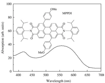
molecular orbital (LUMO) and highest occupied molecular orbital (HOMO) are 3.97 eV and 5.9 eV, respectively. MPPDI is a perylene derivative which exhibits high electron mobility and is commonly used for organic photovoltaic applications[21]. By suitable molecular design, this material has two absorption bands at blue (418 nm) and yellowish-green (557 nm) as shown inFig. 1. The two bands were caused by the absorption of the perylene core, and by the photoinduced intramolecular charge-transfer effect [18], which features charge transfer from aryl substituents to the perylene diimide core due to photon energy absorption, respectively. To achieve an effective destructive interference, a semi-transparent double-metal-layer, Al/Ag, was used to optimize the proportion of transmittance and reflectance to decrease the spectral reflectance from 418 to 557 nm. Hence, a BL-OLED with low reflectance for the whole visible range can be achieved. Notably, the perylene materials are widely applied to organic photo-voltaic devices due to their good electron transport characteristics and high absorption coefficient for visible range. In our BL-OLED, we ob-served that it was sensitive to the ambient light and accompanied a photo-induced current inside the BL part. Such a photo-induced current could separate out electrons and holes by a good structural design, OLEDs integrated on solar cell (reflectance of device ~1.4%–12% with anti-reflection coating)[22], which has the functions applied for power-saving, ambient light detection, and self-brightness-tuning.
2. Experiment
Our OLED fabrication and basic characterization details are outlined in Ref.[14]. The spectroradiometer, Konica Minolta CS1000, and digital source-meter, Keithley 2400, were configured for
measur-ing electroluminescence intensity and spectrum, current density (J) and driving voltage (V) of devices. The spectrophotometer, Hitachi U-4100, was used to measure reflectance of devices from ultraviolet to near infra-red at different wide viewing angles, and A-CR could then be calculated by the following equation[10]:
A−CR =Device luminance OffDevice luminance Onðð Þ + Reflected ambient lightÞ + Reflected ambient light ð1Þ
For studying the photo-current effect of our devices, J-V character-istics under the excitation of a 532 nm green laser were measured by a Keithley 2400 source-meter.
Eleven samples were fabricated with their device structures shown inTable 1. In these devices, we used N, Bis (naphthalen-1-yl) -N, N-bis (phenyl) benzidine (NPB) as the hole-transport layer, Alq3 as the emitting layer and the ETL, LiF as the electron injection layer and Al/Ag/MPPDI/LiF/Al as the BL cathode. The semi-transparent metal consisted of a single Al (Ag) layer or a double metal Al/Ag, which provides efficient destructive interference and an electron injection pathway resulting from the large LUMO difference between Alq3and MPPDI. Between the MPPDI and the Al cathode, an electron injection layer LiF was applied out of necessity for better electron injection from the cathode into MPPDI.
Devices 1 to 4 were designed to study the electron injection and transport characteristics of MPPDI. Workfunctions of electrodes, Ag and Al, are 4.26 eV and 4.28 eV, respectively. Those values are close to the LUMO value of the MPPDI, and far from the HOMO value of the MPPDI. Thus, only the electron current could exist in these four de-vices. Device 5 was a conventional highly reflective bottom-emitting OLED. Devices 6 to 9 had different semi-transparent layer structures, and devices 7,10 and 11 were designed for different MPPDI thicknesses. 3. Results and discussion
3.1. Electrical characteristics
Fig. 2a shows the J-V curves of electron-only devices 1 to 4, where Ag is used as an anode. Fixing the bias at 4 V, the current densities of devices 1 to 4 are 8.27 × 10− 6, 0.0874, 0.341, and 0.0416 A/cm2, respectively. The current density of MPPDI (device 3) is 8.2-times higher than that of Alq3(device 4), which clearly shows the superior electron transport characteristics of MPPDI. By comparing the J–V characteristics of device 2 and 4, we can see that the“intrinsic” carrier transport characteristic of MPPDI is better than that of Alq3. Devices 1 and 3 are designed to study the electron injection characteristics from the electrode into the organic MPPDI layer. A thin LiF layer following the Al electrode (device 3) shows a higher current density than only the Al electrode itself (device 1), which may result from the Li-ion doping effect[23]or a sharp density of states coupling effect of the thin LiF layer[24].Fig. 2b shows the J–V curves of the control device (device 5) and low reflection devices (devices 6 to 11). The thin metal
Fig. 1. Absorption spectrum and chemical structure of MPPDI. (For interpretation of the references to colour in thisfigure legend, the reader is referred to the web version of this article.)
Table 1
Layer structures of the OLED devices
Anode NPB Alq3 LiF Al Ag MPPDI Alq3 LiF Cathode
Device 01
g
Ag 200 500g
Al 1500 Device 02 500 20 5 Device 03 500 5 Device 04 520 5 Device 05g
ITOg
500g
400g
5 1500g
5g
A1 1500 Device 06 50 750 Device 07 25 25 750 Device 08 10 40 750 Device 09 50 750 Device 10 25 25 650 Device 11 25 25 850 Unit:Å.2 T.-L. Chiu et al. / Thin Solid Films xxx (2009) xxx–xxx
layer in the BL structure has to support the destructive interference and achieve a good electrical connection between the front control part and back cathode part in the device. Typically, a LiF/Al bi-layer followed by the ETL, Alq3, would be used for this purpose. However, we found that thinner Al (b50 Å) resulted in voltage increase, and thicker Al (N50 Å) resulted in the increase of reflection. The electrical and optical properties could not be optimized simultaneously. To improve the situation, the Al/Ag bi-layer thin-metal was introduced since Ag has a lower optical absorption and higher electrical con-ductivity than Al. The relative thicknesses of bi-layer thin-metal varied in devices 6 to 9 while the total thickness wasfixed at 50 Å.
Operational voltages, efficiency and reflectance of devices 5 to 11 at 0.05 A/cm2are listed inTable 2. Driving voltages of devices 6, 7 and 8 were nearly identical, which were about 0.55 V higher than control device 5 due to the increase of the BL thickness. Although the BL
thicknesses of devices 6, 7 and 8 were 84% thicker than control device 5, the driving voltages of these devices rose by only 8%, which proves the high conductivity of MPPDI. Device 9 has a very high driving voltage since LiF/Ag cannot provide an efficient electron injection pathway from the metal to the ETL[23]. Therefore, we can conclude that: (1) an Al layer is essential with the structure Alq3/LiF/Al for better electron injection from the cathode to the ETL, and that (2) regardless of the thickness ratio of Al/Ag layer, the total thickness of 50 Å for the Al/Ag layer is sufficient to provide an efficient electrical connection between the control part and the BL cathode. Devices 10 and 11, combined with device 7, were used to study the effects of the thickness of MPPDI. The driving voltage increased with the MPPDI thickness. However, the operational voltage of device 11 was 0.7 V, higher than device 10 at 0.05 A/cm2, although the MPPDI in device 11 was 200 Å thicker than in device 10. This means that the conductivity of the MPPDI provides a margin for optimizing the optical characteristics. As shown inTable 2, the current efficiency of device 5 is about double those of devices 6, 7, and 8, since part of the OLED emission was absorbed by the black layer. The efficiency of device 9 was quite low due to the bad electron injection and poorly balanced carrier.
3.2. Optical performance
Fig. 3a shows the reflectance spectra of devices 5 to 9. The control device 5 has a much higher spectra reflectance than the others, which could be easily obtained due to highly reflective Al cathode. The spectral reflectances from devices at 555 nm, which is the most
Table 2
Electrical and optical properties of devices 5 to 11
Operational voltage⁎ Efficiency⁎ Luminance
(V) (cd/A) Reflectance⁎⁎ (%) Device 05 6.9 2.7 77.6 Device 06 7.5 1.4 23.3 Device 07 7.5 1.24 6.3 Device 08 7.4 1.28 14.3 Device 09 10.3 0.023 17 Device 10 7.2 1.5 33 Device 11 7.9 1 8.9 ⁎measured at 0.05 A/cm2 . ⁎⁎measured at 555 nm.
Fig. 3. Reflectance spectra of (a) devices 5 (control OLED), and 6 to 9 (BL-OLED devices with different Ag/Al proportion of intra semitransparent metal layer), and (b) devices 7, 10, and 11 (BL-OLED devices with different MPPDI thickness).
Fig. 2. J–V characteristics of (a) devices 1 to 4, and (b) devices 5 to 11.
3 T.-L. Chiu et al. / Thin Solid Films xxx (2009) xxx–xxx
sensitive wavelength to human eye, are also listed inTable 2. Changing the relative thicknesses of the Al/Ag bi-layer effectively modulated the absorption, transmission, and reflection of the thin-metal, while the absorption of the MPPDI remained constant. As the thickness of the Ag increased, the reflectance at 555 nm decreased and then increased, which means that the destructive interference is most effective when the Ag was 25 Å thick.Fig. 3b shows the reflectance spectra of device 7, 10, and 11. The reflectances at 555 nm of devices 7, 10, and 11 were 6.3%, 33%, and 8.9%, respectively. The reflectance of device 10 was higher than devices 7 and 11 due to the thinner MPPDI and lower absorption. On the other hand, thicker MPPDI (850 Å), did not cor-respond to the lowest reflectance, because both absorption of organic material and destructive interference of microcavity structure should be taken into consideration simultaneously. With thicker MPPDI, the absorption of BL structure is stronger and the light intensity reflected back (passing through MPDI twice) from the cathode is lower. It results in a less effective destructive interference effect with the light directly reflected back from the double metal structure. In our case, combining the material absorption and cavity structure, the optimized condition happens at device 7 (MPPDI 750 Å).
According to Eq. (1), the A-CR of these devices can be calculated based on their measured reflectance spectra (R(λ)) in Fig. 3. The reflected ambient in Eq. (1) was defined as ∫700nm
350nmVð ÞS λλ ð ÞR λð Þdλ=∫ 700nm
350nmVð ÞS λλ ð Þdλ, where V(λ) is the standard
photometric spectrum and S(λ) is the spectrum of illuminant[4,15], here we chose a standard illuminating source (daylight spectrum with color temperature 6500K, D65). The A-CR of devices 5 (control), 6 (Al metal layer), and 7 (Al/Ag double metal), withfixed device brightness at 600 cd/m2and illumination of ambient light at 1000 lx, were calculated as 3.49, 16.83, and 26.74, respectively. The values of the A-CR of devices 6 and 7 were 4.82 and 7.85 times higher than the A-CR of a conventional device (device 5).
Reflectance spectra of device 7 at different viewing angles are shown inFig. 4. Surface reflection of the air/glass interface increases with larger viewing angles which accounts for the reflectance increase inFig. 4. The minimum reflectance 4.7% near 450 nm was observed at 0°view angle, which is much lower than the minimum 5% reflectance of previous work without anti-reflection (AR) coating. The reflections from the air/glass interface at viewing angle 0°, 20°, 40°and 60°are 4%, 4.03%, 4.57% and 8.92%, respectively, from Fresnel reflectance calcula-tion [25]. Corrected reflectance spectra could be obtained by subtracting the surface reflection value fromFig. 4. It is noteworthy that the minimum corrected reflectance at 0° is as low as 0.7% at 450 nm, which is much lower than the minimum reflectance (~1.4%) with AR coating of previous work by Yang et al[22]. Since our BL-OLED
consists of absorptive MPPDI and a double-metal semitransparent layer, the reflectance value can be kept at a low value, even when observed at different viewing angles.
Fig. 5shows the photos of devices 5 and 7 at different viewing angles under a 500 lx ambient illumination with the spectrum shown in the inset ofFig. 4. The bright patterns including pixels and electrical circuits result from strong cathode metal reflection at different viewing angles. It is clear our BL-OLED maintains the high contrast properties at a wide viewing angle.
3.3. Photosensitive effect and reliability
According to several studies of perylene derivatives reported earlier, MPPDI is supposed to respond to photo-excitation[21]. In particular, MPPDI, in a phase changing layer and in an absorption layer, is easily excited by ambient or emission light. With suitable device design to separate electron-hole effectively, this BL-OLED has the potential to convert the optical energy to an electrical one[22]. To study such a photosensitive effect simply, we used a 532 nm green laser because MPPDI has a strong absorption band from green to yellow, beingfixed at 60 mW/cm2, to pump the low reflection devices. Here, we define the percentage of photocurrent enhancement (PPE) at a specific voltage as the current density difference between the bright and dark conditions over the current density under the dark con-dition, PPE = ( Jbright−Jdark)/Jdark. The PPE of control- and BL-OLED variation with driving voltage was shown inFig. 6. The PPE of devices 7, 10, and 11 at bias 3.6 V were 15.6%, 12.6%, and 13.3%, respectively. On
Fig. 4. Reflectance spectra at different viewing angles for device 7 (BL-OLED).
Fig. 5. Photos of control- (devices 5), and BL-OLED (devices 7) at different viewing angles.
Fig. 6. The percentage of photocurrent enhancement (PPE) under different bias voltage for device 5, 7, 10 and 11.
4 T.-L. Chiu et al. / Thin Solid Films xxx (2009) xxx–xxx
the contrary, device 5, which only contains NPB and Alq3, did not absorb 532 nm photons and showed no PPE effect. Device 7 exhibited a highest PPE value due to its lowest reflection, namely, device 7 absorbed more energy than the others.
Fig. 7shows the operational stability results for devices 5 and 7 by using accelerating lifetime measurement driven by a constant current density of 100 mA/cm2. Their initial luminances were 2689 and 1558 cd/m2for device 5 and 7, respectively. The smooth and slowly declining curves of normalized brightness for reference device and BL one were nearly identical after 32 h operational aging test. Obviously, the BL device demonstrated a comparable stability to the reference device, and their half-lifetimes 92.77 and 93.86 h could be estimated by extending the slope of the tail to reach the half initial emitted intensity under continuous driving. This result shows that the extra MPPDI layer has little effect on the operation lifetime of a BL-OLED. 4. Conclusion
In summary, we demonstrated a low-reflection BL-OLED with 6.3% reflectance at 555 nm (12 times smaller than the control device) by using MPPDI for the phase changing and the light absorbing layers, and using double-metal-layer (Al/Ag) as a semi-transparent layer to control the ratio of transmission and reflection. The thickness of the MPPDI was varied to modulate the destructive interference effect for minimum spectral reflectance. Due to its high conductivity, the driving voltage of the optimized low-reflection BL-OLED (Device 7) was only 0.55 V higher than the control device (Device 5) although an
extra 750 Å MPPDI layer was inserted inside this device. The A-CR of the low-reflection BL-OLED was 26.7, which is 7.85 times higher than the conventional one (device 5) at the condition that device emitted brightness 600 cd/m2 under 1000 lx illumination of ambient light (D65). The reflectance values were kept low at different viewing angles due to combining absorption and destructive interference. In addition, the maximum photocurrent enhancement of the optimized low-reflection OLED (Device 7) was 15.6% at 3.6 V and there was no photocurrent observed in the control device (Device 5). This pho-tosensitive characteristic of MPPDI clearly leads to power-saving, ambient light detection, and self-brightness-tuning with suitable structural design of the device.
Acknowledgments
Authors acknowledge with great appreciation thefinancial support provided by CHIMEI Optoelectronics Corporation and by the National Science Council, R.O.C., under Grant NSC 96-2221-E-002-126, NSC 97-2221-E-002-056 and NSC 96-2113-M-002-001.
References
[1] C.W. Tang, S.A. Vanslyke, Appl. Phys. Lett. 51 (1987) 913. [2] L.S. Hung, C.H. Chen, Mater. Sci. Eng. R 39 (2002) 143. [3] L.S. Hung, J. Mandathil, Adv. Mater. 13 (2001) 1787. [4] Z. Wu, L. Wang, Y. Qiu, Opt. Express 13 (2005) 1406.
[5] C.C. Wu, C.W. Chen, C.L. Lin, C.J. Yang, J. Disp. Technol. 1 (2005) 248.
[6] F.L. Wang, M.K. Fung, X. Jiang, C.S. Lee, S.T. Lee, Thin Solid Films 446 (2004) 143. [7] H. Aziz, Y.F. Liew, H.M. Grandin, Z.D. Popovic, Appl. Phys. Lett. 83 (2003) 186. [8] H.M. Grandin, H. Aziz, S. Gardner, C. Jennings, A.J. Paine, P.R. Norton, Z.D. Popovic,
Adv. Mater. 15 (2003) 2021.
[9] S.H. Li, H. Liem, C.W. Chen, E.H. Wu, Z. Xu, Y. Yang, Appl. Phys. Lett. 86 (2005) 143514. [10] K.C. Lau, W.F. Xie, H.Y. Sun, C.S. Lee, S.T. Lee, Appl. Phys. Lett. 88 (2006) 083507. [11] X.D. Feng, R. Khangura, Z.H. Lu, Appl. Phys. Lett. 85 (2004) 497.
[12] Z.Y. Xie, L.S. Hung, Appl. Phys. Lett. 84 (2004) 1207.
[13] Y.C. Zhou, L.L. Ma, J. Zhou, X.D. Gao, H.R. Wu, X.M. Ding, X.Y. Hou, Appl. Phys. Lett. 88 (2006) 233505.
[14] J.H. Lee, C.C. Liao, P.J. Hu, Y. Chang, Synth. Met. 144 (2004) 279. [15] W.F. Xie, Y. Zhao, C.N. Li, S.Y. Liu, Opt. Express 14 (2006) 7954.
[16] W.F. Xie, H.Y. Sun, C.W. Law, C.S. Lee, S.T. Lee, S.Y. Liu, Appl. Phys., A Mater. Sci. Process. 85 (2006) 95.
[17] J.H. Lee, J.J. Huang, C.C. Liao, P.J. Hu, Y. Chang, Chem. Phys. Lett. 402 (2005) 335. [18] C.C. Chao, M.K. Leung, Y.O. Su, K.Y. Chiu, T.H. Lin, S.J. Shieh, S.C. Lin, J. Org. Chem. 70
(2005) 4323.
[19] F. Dinelli, R. Capelli, M.A. Loi, M. Murgia, M. Muccini, A. Facchetti, T.J. Marks, Adv. Mater. 18 (2006) 1416.
[20] D.J. Gundlach, K.P. Pernstich, G. Wilckens, M. Gruter, S. Haas, B. Batlogg, J. Appl. Phys. 98 (2005) 064502.
[21] P. Peumans, A. Yakimov, S.R. Forrest, J. Appl. Phys. 93 (2003) 3693. [22] C.J. Yang, T.Y. Cho, C.L. Lin, C.C. Wu, Appl. Phys. Lett. 90 (2007) 173507. [23] C.I. Wu, G.R. Lee, T.W. Pi, Appl. Phys. Lett. 87 (2005) 212108.
[24] Z.H. Lu, R.S. Khangura, M.W.C. Dharma-wardana, M.Z. Zqierski, D. Ritchie, Appl. Phys. Lett. 85 (2004) 323.
[25] B.E.A. Saleh, M.C. Teich, Fundamental of Photonics, John Wiley & Sons, New York, 1991.
Fig. 7. Accelerated lifetime measurements of control- (devices 5) and BL- OLED (devices 7).
5 T.-L. Chiu et al. / Thin Solid Films xxx (2009) xxx–xxx