Superior Damage-Immunity of Thin Oxides
Thermally Grown on Reactive-Ion-Etched
Silicon Surface in
N 2 0Ambient
S. Y. Ueng, T. S. Chao, P. J. Wang, W. H. Chen, D. C. Chang, and H. C. ChengAbstract-Thin oxides thermally grown on reactive-ion-etched silicon surfaces in N20 ambient have been studied. As compared with pure oxides grown on the etched silicon in dry oxygen, 3720-grown oxides exhibit significantly stronger immunity to the RIE-induced damages. A great improvement in both time-zero-dielectric-breakdown (TZDB) and time-dependent-breakdown (TDDB) characteristics is observed for the NZO-grown oxides on RIE-treated silicon surfaces. Accelerated tests have shown that the N 2 0 oxide grown on the RIE silicon surface can achieve a lifetime longer than the pure oxide grown on the correspondingly etched silicon surface with a factor over lo*.
I. INTRODUCTION
As device dimensions get smaller, a high definition etching tech- nique, such as reactive ion etching (ME), is required. Hence, the effects of RIE processes have been widely studied for the ultra-large- scale-integrated (ULSI) technology. For advanced semiconductor devices, such as tunnel oxides for electrically erasable read-only memory (EEPROM) devices and dielectrics for trench capacitors, thin thermal oxides are frequently grown on a RIE-treated silicon surfaces. Due to the ion bombardment, the induced damages in the silicon can not be avoided during the dry etching. The quality of thin thermal oxides grown on the RIE-treated silicon will be therefore degraded by these residual defects. Many authors [I], [2] have studied on the issues of damages induced by the RIE. On the other hand, the benefits of Nz 0-grown oxides have also been extensively studied in the past few years. Strong interface stability, low electron traps, and large charge-to-breakdown have been observed by many authors [3],
[4] for the NzO oxides. In this letter, the damage-immunity of the thin oxide grown on the reactive-ion-etched silicon surface in N2O ambient will thus be proposed.
11. EXPERIMENTAL PROCEDURES
(100) oriented, 2.5-3.5 a - c m , boron-doped silicon wafers were used. At first, 350A-thick oxides were grown in 0 2 ambient at 900°C. To introduce the damages on the silicon surface, the oxide stripping was performed by a RIE system. A two-step oxide-etching recipe using CHF3/CF*/Ar and CF4/02 was employed. After the oxide etching, thermal oxides (-80
A)
were grown at 900°C in N 2 - diluted 0 2 and wholly N 2 0 ambient, respectively. Some samples without RIE treatments were accompanied for each run to evaluate the impacts of the defects induced by the RIE. Subsequently, an in situ post-oxidation annealing was performed in NZ ambient at 900°C for10 min. After a 4000A-thick polysilicon deposition and subsequent
POC13 diffusion, MOS capacitors were fabricated to analyze the characteristics of the dielectrics.
Manuscript received July 27, 1993; revised November 15, 1993. The review
of this brief was arranged by Associate Editor K. Tada.
S . Y. Ueng and H. C. Cheng are with the Department of Electronics Engineering and Institute of Electronics, National Nan0 Device Laboratory, National Chiao Tung University, Hsinchu, Taiwan, R.O.C.
T. S. Chao, P. J. Wang, W. H. Chen, and D. C. Chang are with the National Nan0 Device Laboratory, National Chiao Tung University, Hsinchu, Taiwan, R.O.C.
IEEE Log Number 92 15974.
IEEE TRANSACTIONS ON ELECTRON DEVICES, VOL 41, NO.
I
I
5, MAY 1994
0
4
8
12
1620
Fox
(MV/cm)
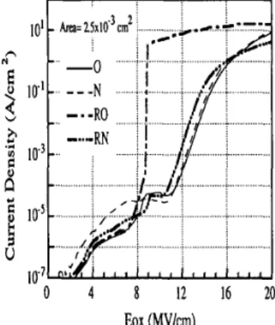
Fig. 1.by the voltage ramping technique with a ramping rate of 1 V/s.
Curves of current density ( 1 ) versus electrical field ( E o x ) obtained
111. RESULTS AND DISCUSSION
In order to avoid the effects of high-temperature annealing, pure oxides were grown in N2-diluted 0 2 ambient to keep the oxidation time comparable to that for the N20-oxidation process. The time for dry oxidation and NzO-oxidation are 85 min and 78 min, accordingly. The dependence of current density
( J )
on electrical field (E o x )
for different dielectrics are shown in Fig. 1. It is clearly noted in this figure that the sample RO, with pure oxide grown on the RIE-treated silicon, exhibits a remarkable degradation. Due to the ion bombardment from RIE, contaminations and damages will be induced on the silicon surface [ 5 ] , [6]. As is well known, surface stacking faults via the contaminations can occur after high- temperature oxidation for RIE samples, which degrade the oxide breakdown voltages [ 5 ] . Therefore, the damages induced by RIE is conjectured as the main cause for the early breakdown events of the sample RO. On the contrary, the sample RN, i.e., N20-oxide grown on the RIE-treated silicon, displays a great improvement over the sample RO in the leakage currents and breakdown fields. It indicates that thermal oxides grown on the RE-treated silicon surface in Nz 0atmosphere can remedy the RIE-induced defects. The cumulative distributions of TZDB characteristics for various dielectrics are shown in Fig. 2. Oxide breakdown field ( E b d ) , is defined as the electrical
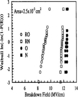
field at which the gate current reaches to 1 mA/cni2. For the samples without RIE, pure oxide, 0, and N 2 0 oxide, N, show no difference in TZDB characteristics. These results were consistent with what have been reported [3], [4] that NzO-grown oxides and pure oxides have similar TZDB characteristics. However, for the RIE-treated specimens, the sample RN possess higher breakdown fields and tighter distribution than the sample RO. Furthermore, the breakdown field and its distribution of the sample RN are similar to those of the sample N and 0. Lots of AES and SIMS [7] data have shown that nitrogen pileup near the interface exists for the N20-grown oxides. It is believed that these nitrogen atoms must play an important role to passivate the RIE-induced damages.
Fig. 3 shows the time-to-breakdown ( f B D ) characteristics of the
MOS capacitors (area = 1.6 x lop3 mi2) for various dielectrics under a constant voltage stressing of 13 MV/cm. The sample 0 and also show a narrow-range distribution and little difference in f B D ,
as was reported by other authors [3]. It indicates that the oxidation
IEEE TRANSACTIONS ON ELECTRON DEVICES, VOL. 41, NO. 5, MAY 1994 85 1 0 0 0
RO
D U R N 0 0 lo t N n 0 on D 0 0 6 8 IO I2 14 Breakdown Field (MV/cm)Fig. 2. Cumulative probabilities of the time-zero dielectric-breakdown char- acteristics using voltage ramping technique for the MOS capacitors with an area of 2.5 x cm’. Breakdown field is defined as the field at which the gate current density reaches to 1 mA/cmZ.
1
Constant Voltage Sbessing : 13 W/cm
Y
o m
0 .I
-
io1 I@ io1
id
id
io4
Time-lo-Breakdown (sec)Fig. 3. Weibull plots of the time dependent dielectric breakdown (TDDB) characteristics at a constant stressing electrical field of 13 MV/cm for the capacitors with various dielectrics.
environment, including initial cleaning and device fabrication, is normal in this experiment. On the other hand, the RE-treated samples show a significant difference between pure oxides and NzO-grown oxides in TDDB characteristics. From the data, no capacitor of the sample RO survives over
lo-’
s with a constant field stressing at 13 MV/cm. In contrast, the sample RN exhibits a tolerable range of t B D and a distribution for practical applications. According to the TDDB model [8], the early breakdown is caused by the weak spots from the high density of hole traps at the cathode, thinner oxide thickness, lower barrier height due to the contamination, or crystalline defects. The improved TDDB characteristics of NzO-grown oxides are at- tributed to the nitrogen pileup at interface with reducing dangling bond densities of Si and strained Si-0 [3]. Therefore, the weak spots at the SiOz/Si interface caused byR E
treatment are strengthened.In order to compare the lifetime of NzO oxides and pure oxides grown on the RIE-treated Si surface, accelerated TDDB tests [9] were demonstrated. The log ( f B D ) versus 1/E plots of the sample RO and
RN are shown in Fig.
4.
The slopes, G, of the projection lines for the sample RO and RN are 360 MV/cm and 352 MV/cm, respectively. They are close to the data reported by Chen et al. (320 MV/cm) [ 101. The dielectric lifetimes of the sample RO and RN were then projected by extrapolating the TDDB projection curve at the Eos = 8 MV/cm. The f B D of the sample RN is estimated to have about nine orders as large as that of the sample RO.IV. SUMMARY AND CONCLUSIONS
Thin NzO-oxides grown in N 2 0 ambient have been shown to exhibit superior immunity to the RIE-induced damages than pure oxides. This process could provide higher breakdown fields, lower leakage current, and significantly improved TDDB characteristics for the thermal oxides on the RE-treated silicon substrates. The NzO-oxides grown on the etched Si surface could achieve a quality comparable to the thermal oxides grown on nonetched wafers. Therefore, NzO-grown oxides will be a promising candidate for the future ULSI application, especially the subsequent oxidation after the RIE process.
ACKNOWLEDGMENT
The authors wish to take this opportunity to gratefully acknowledge many helpful discussions with H. P. Su. Technical support from National Nan0 Device Laboratory (NDL) of ROC NSC is also acknowledged.
REFERENCES
S. W. Pang, D. D. Rathman, D. J. Siliversmith, R. W. Mountain, and
P. D. DeGraff, “Damage induced in Si by ion milling or reactive ion etching,” J. Appl. Phys., vol. 54, no. 6, pp. 3272, 1983.
X. C. Mu, S. J. Fonash, G. S. Oehrlein, S. N. Chakravarti, C. Parks, and J. Keller, “A study of CClF3/H2 reactive ion etching damage and contamination effects in silicon,” J. Appl. Phys., vol. 59, no. 8, p. 2958,
1986.
W. Ting, G. Q. Lo, J. Ahn, and D. L. Kwong, “MOS characteristics of ultrathin Si02 prepared by oxidizing Si in N z 0 , ” IEEE Electron Device Lett., vol. 12, p. 416, 1991.
W. Ting, G. Q. Lo, J. Ahn, T. Chu, and D. L. Kwong, “Comparison of dielectric wear-out between oxides grown in 0 2 and N z 0 , ” Proc. IEEE Reliability Phys. Symp., 1991, p. 323.
F. K. Moghadam and X.C. Mu, “A study of contamination and damage on Si surfaces induced by dry etching,” IEEE Trans. Electron Devices, vol. 36, p. 1602, 1989.
H. P. Strunk, H. Cerva, and E. G. Mohr, “Damage to the silicon lattice by reactive ion etching,” J. Electrochem. Soc., vol. 135, p. 2877, 1988.
G. Weidner and D. Kruger, “Nitrogen incorporation in Si02 by rapid thermal processing of silicon and Si02 in N20,” Appl. Phys. Lett., vol.
62, p. 294, 1993.
I. C. Chen, S. Holland, and C. Hu, “Electrical breakdown in thin gate and tunneling oxide,” IEEE Trans. Electron Devices, vol. ED-32, p. 413, 1985.
I. C. Chen and C. Hu, “Accelerated testing of time-dependent breakdown of Si02,” IEEE Electron Device Letr., vol. 8, p. 140, 1987.