行政院國家科學委員會專題研究計畫 期中進度報告
子計畫六:奈米製程之低電壓類比濾波器設計(2/3)
計畫類別: 整合型計畫
計畫編號: NSC93-2220-E-009-019-
執行期間: 93 年 08 月 01 日至 94 年 07 月 31 日
執行單位: 國立交通大學電信工程學系(所)
計畫主持人: 洪崇智
共同主持人: 吳介琮
計畫參與人員: 羅天佑, 莊誌倫, 張家瑋, 楊峻岳, 邱俊宏, 李三益
報告類型: 完整報告
報告附件: 出席國際會議研究心得報告及發表論文
處理方式: 本計畫可公開查詢
中 華 民 國 94 年 5 月 30 日
行政院國家科學委員會補助專題研究計畫
□ 成 果 報 告
█ 期中進度報告
奈米製程之低電壓類比濾波器設計(2/3)
計畫類別:□
個別型計畫 █
整合型計畫
計畫編號:NSC 93-2220-E-009-019
執行期間:2004 年 8 月 01 日至 2005 年 7 月 31 日
計畫主持人:
洪崇智 國立交通大學電信工程學系
共同主持人:
吳介琮 國立交通大學電子工程學系
計畫參與人員:
羅天佑, 莊誌倫, 張家瑋, 楊峻岳, 邱俊宏, 李三益
成果報告類型(依經費核定清單規定繳交):█精簡報告 □完整報告
本成果報告包括以下應繳交之附件:
□赴國外出差或研習心得報告一份
□赴大陸地區出差或研習心得報告一份
▉出席國際學術會議心得報告及發表之論文各一份
□國際合作研究計畫國外研究報告書一份
處理方式:除產學合作研究計畫、提升產業技術及人才培育研究計畫、列
管計畫及下列情形者外,得立即公開查詢
□涉及專利或其他智慧財產權,□一年□二年後可公開查詢
執行單位:國立交通大學電信工程學系
中 華 民 國 94 年 5 月 28 日
奈米製程之低電壓類比濾波器設計(2/3)
計畫編號:NSC 93-2220-E-009-019
執行期限: 2004年8月01日 至 2005年07月31日
主持人:洪崇智 國立交通大學電信工程學系
I. 中文摘要
隨著行動通訊的盛行,低功率的積體電路顯得日益重要。對於數位電路而言,消耗功
率主要和供應電壓、操作頻率、負載電容有關,所以降低供應電壓變成一種趨勢。通常操
作在低供應電壓時,數位電路的功能能受到的影響有限;然而對於類比電路設計而言,動
態範圍往往會受到供應電壓的降低,而受到大幅的限制。由於為了將數位電路和類比電路
整合在一起,因此我們必須發展新的低電壓類比電路技術。由於電晶體將以深次微米的技
術來製造,相比較之前的技術而言,電晶體可能將會呈現不同的電子特性,所以我們先了
解深次微米技術所產生的電晶體特性,再依所得知的模型為基礎做相對應的設計。在此年
度的執行計畫中,我們以現有的前瞻性製程研究應用於低電壓的取樣開關,在接下來的計
畫中,我們會將它應用至切換式電容低壓濾波器,並經由適當的電路設計與架構建立,完
成整個濾波電路。
關鍵詞:低功率、低電壓、類比積體電路、動態範圍、切換式電容濾波器
Abstract
As there is a great demand for lighter hand-held mobile phones, low power IC circuit
design solutions must be developed. For digital circuits, the power consumption is mainly
relative to power supply voltage, operating frequency and loading capacitor. It is a trend to
reduce the power supply. In the most case, the digital circuit is usually not affected too much.
On the other hand, for analog circuits, the dynamic range is strongly affected by the low
voltage supply. Based on the concept of System-on-chip, new design techniques for
low-voltage analog circuits are required to be developed. Since the transistors fabricated by
the deep sub-micron technology might exhibit different electrical characteristics, as compared
with the previous larger feature-size technologies, the study of the transistor characteristics in
the process is needed. We developed a new sampling switch applied in low voltage based on
advanced process technology. In later part of the proposal, we will apply the sampling switch
in the switched capacitor filter. After establishment of moderate circuit and architecture design,
we complete the switched capacitor filter.
II. 前言及研究目的
在近幾年來,低操作電壓積體電路日益盛行,其操作電壓已經下降至 1.8V 之下,工作
於低操作電壓的濾波器也因此為一項重要的研究主題。隨著射頻收送器整合程度的上升,
互補式金屬氧化層半導體的技術將會最符合其經濟效益。對於應用於高頻段的 CMOS 射頻
電路來說,深次微米的製程呈現了非常好的效能,同樣的,數位電路也使用了相同的製程。
基於系統單晶片的概念,對於類比濾波器來說,我們也需要應用於深次微米技術的低電壓
解決方案。
此研究主要的目的,在於使用深次微米之技術來發展低電壓切換式電容濾波器。通常
在 SC-filter 中,會使用到大量的電晶體開關(switch)。而在低供應電壓的狀態下,電晶體
開關會受到供應電壓下降而使得擺幅範圍(swing range)受到相當大的限制,同時由於 swing
range 變小,也會使得整個電路的動態範圍(Dynamic range)下降許多。因此在低電壓的情
況下設計 SC 的電路將是一個很大的挑戰。同時由於單純的電晶體關關,會產生較大的失
真,如何降低失真以提升 Dynamic range 則是我們此次計畫的重點。因此如何利用此深次
微米技術,並降低工作電壓來實做出所需的低電壓濾波器,則是本計畫主要的目標。
此年度部分的設計著重於建立符合現況所需之低電壓低失真的電晶體開關。在確定了
製程技術之後,我們藉由數學的推導和 Hspice 的模擬分析來完成此低電壓低失真的電晶
體開關。此基本開關使用了 TSMC 0.18um 的製程做模擬並可以操作在低壓同時產生較低
的失真。我們相信將此應用在 SC 的電路上,再加以整合並做系統上的改良,將能對於本
計畫下年度的研究,提供關鍵性的貢獻。
本報告的第三部份將討論本計畫的研究方法及成果,第四部份則為結論與討論。實做
部分則陸續下線整理,同時我們的研究成果也被 ISCAS 2005 所接受,並於今年五月受邀發
表[1]。
III. 研究方法及成果
研究方法及成果主要為建立一個可操作在一個低電壓的低失真開關。Figure1.為一個常見
的簡單取樣開關。我們可以發現取樣開關輸出的電壓會被限制在 Vdd-Vt,當供應電壓下降
時,整個開關的輸出範圍也會減少,進而使得動態範圍變小。所以我們必須設法設計一個可
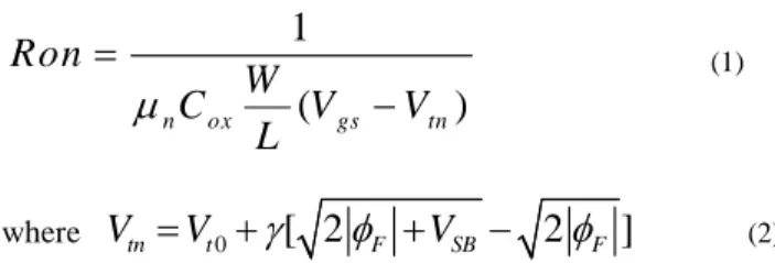
以操作在低電壓的開關,同時也能提供較大輸出範圍。同時方程式(1)則表示了開關的取樣電
阻,為了要降低諧波失真,我們同時也必須設法使得整個開關的取樣電阻和輸入信號無關以
降低諧波失真。
1
(
)
n ox gs tnRon
W
C
V
V
L
µ
=
−
(1)
為了要使得開關能夠操作在低電壓的狀態,我們採用了 bootstrapped switch 的架構。
Bootstrapped switch 是常見於低電壓的 SC 電路。它能夠提供較大的輸出範圍,同時還能夠
提供較小的諧波失真。我們所發展的取樣開關也是以 bootstrapped switch 做為我們的研究
基礎並加以改進。Figure2 則是 bootstrapped switch 的示意圖。在 o1 時,開關 3、4、5 會
被關上,而電容則會被充電至 vdd 的準位,此時由於取樣開關的閘極接地,所以開關是處在
off 的狀態。而在 o2 時,開關 1、2 會被關上,此時取樣開關的閘極被充電至 vdd+vin,開關
處在取樣的狀態。我們可以發現它的 Vgs 為一個 vdd。將它代入(1)中,我們可以得到它的取
樣電阻為
1
(
)
n ox tRon
W
C
Vdd V
L
µ
=
−
(2)
同時我們可以發現在取樣電阻中所有的參數均和輸入信號無關,可以有效地降低諧波失
真。不過我們也可以發現此電路的一個問題。對一個 n 型的取樣開關,當先前輸出的取
樣信號小於輸入信號時,電晶體源極會被交換到輸出端,此時輸入端不再是源極,而使
得其 Vgs 不完全等於 vdd 而使得取樣開關的線性度受到影響。
基底效應補償(body effect compensation)
雖然我們可以設法使得取樣開關的 Vgs 成為固定常數,但是取樣電阻中的 Vt 依舊會受到基底
效應(body effect)影響,而使得開關的線性度下降。因此我們需要一些基底效應補償(body
effect compensation)的技術,來提升整個電阻的線性度。Figure3.為一種常見的 replica
compensation 的方法。我們利用一個相同於取樣開關的電晶體(MD)來做補償。我們可以發現
當電晶體 MD 處在飽和區時,它汲極電流為
21
(
)
2
D n ox GS tW
I
C
V
V
L
µ
=
−
所以我們可以得到 Vgs
1
(
)
2
D G S t n o xI
V
V
W
C
L
µ
=
+
因為放大器採用負回授的架構,所以 replica 電晶體的源極電位為 Vin。所以我們可以得到
1
(
)
2
D G t in n o xI
V
V
V
W
C
L
µ
=
+
+
最後可以得到它的取樣電阻為
1
2
(
)
(
)
D n ox dd n ox MDRon
I
W
C
V
W
L
C
L
µ
µ
=
+
我們可以發現它的所有參數已經和輸入信號無關。
不過此種補償方法主要有兩種缺點:
1. 輸入範圍變小。
2. Vt 難以完全補償。
由於我們使用 replica 電晶體來做為補償,因此我們必須讓它處在飽和區,上述的推導才會
成立。所以電晶體的 Vgs 必須大於 Vt,同時也會造成輸入的範圍被限制在 Vdd-Vt,這不是我
們所希望的。同時由於製程的漂移和二階效應(channel length modulation)的影響,都會使
得整個補償的效果不完全。
綜合以上的分析,我們得到了以下的想法:
由於開關的源極是一直在變化的,我們需要找出真正的源極以確保整個取樣開關的 Vgs 完全
等於 Vdd,同時我們決定採用將 source 和 bulk 連接的方法來取代 replica compensation。
這是因為 Vbs 為 0v 時,電晶體會擁有最好的線性度,也不會補償不完全的問題,同時還可以
使得整個取樣開關有較大輸出入範圍。
Figure4.則是我們所提出的電路,我們用了一個比較器來決定開關 6、7 的連接與否,而開關
1234 和電容則是提供 voltage boosting。我們以 P 型的取樣開關為例,可分為兩種情形討論:
1.當 Vin > Vout 時,取樣開關的真正源極為輸入端,此時開關 6 會被關上,我們可以發現
source inV
=
V
,V
gate=
V
in−
V
dd ,V
tp=
V
t0 ,V
sg=
V
dd 01
(
)
p ox dd tRon
W
C
V
V
L
µ
=
−
2.當 Vin < Vout 時,取樣開關的真正源極變為輸出端,此時開關 7 會被關上,我們可以發現
source outV
=
V
,V
gate=
V
out−
V
dd,V
tp=
V
t0,V
sg=
V
dd 01
(
)
p ox dd tRon
W
C
V
V
L
µ
=
−
我們可以發現所有取樣電阻已經和輸入信號無關同時擁有較高的線性度以及較大的輸出入範
圍。
Vout Vin Vdd Vdd Vdd SW1(Ø2) SW2(Ø1) SW3(Ø1) SW4(Ø2) SW5(Ø1)
Figure3. Transistor replica compensation
MD +
-GV
SV
DI
模擬結果
Figure5 則為我們的模擬結果。(a)為我們的輸入信號,(b)則為我們的輸出信號。根據我們
之前的想法,bulk 會和真正的源極連接,也就是會找出輸出入端中電壓較高的一端。所以我
可以看見(c)的信號則會繪出(a)和(b)中電壓較高的部份。Figure6 則是三種不同取樣開關的
FFT。
(c)FFT of the output in the proposed circuit
(b)FFT of the output in the ref[3]
(a)FFT of the output using bootstrapped switch without compensation
第 一 種 則 為 普 通 bootstrapped switch , 第 二 種 則 為 採 用 replica compensation 的
bootstrapped switch,而第三種則是我們所提出的取樣開關。我們可以從 Table1 中發現到
我們所提出的開關提供了一些效能上的改進。
Table 1. Simulation results for harmonic distortion
Typical Ref[3] Proposed
THD -41.6db -71.8db -84.1db HD2 -44.2db -72.7db -87.9db HD3 -46.9db -82.6db -105.9db
IV. 結論與討論
本年度計畫已順利完成主要的工作項目,我們提供了一個可操作在低電壓,具有較大的
輸出入範圍和低失真的取樣開關。我們可以藉由這個我們所發展的取樣開關來做為我們 SC
filter 的基本元件,用以提升這個切換式開關電容濾波器的動態範圍(Dynamic range)。
V. 參考文獻
[1]Chun-Yueh Yang and Chung-Chih Hung ,”A Low Voltage Low Distortion Sampling Switch”
Proceedings of the 2005 IEEE International Symposium on Circuits and Systems, pp3131-3134 ,
May 23 – May 26, 2005
.
[2] J. Steensgaard, , ”Bootstrapped low-voltage analog switches,” Proceedings of the 1999 IEEE
International Symposium on Circuits and Systems, Volume 2, pp.29- 32, May 30 – June 2, 1999.
[3]A.K. Ong, V.I. Prodanov, and M. Tarsia, ”A method for reducing the variation in “on” resistance
of a MOS sampling switch,” Circuits and Systems, 2000. Proceedings. ISCAS 2000 Geneva. The
2000 IEEE International Symposium, Vol.5, 28-31, pp.437 – 440, May 2000
[4] Kim Sangwook and Greeneich, ”Body effect compensated switch for low voltage
switched-capacitor circuits,” Proceedings of the 2002 IEEE International Symposium on Circuits
and Systems, Volume 4, pp.437-440, May 26-29, 2002.
[5] S. R. Sonkusale and J. Van der Spiegel, ”A low distortion MOS sampling circuit,” Proceedings
of the 2002. IEEE International Symposium on Circuits and Systems, Volume 5, pp.585-588 ,
May 26-29, 2002.
[6] A. M. Abo and P. R.Gray, “A 1.5-V, 10-bit, 14.3-MS/s CMOS pipeline analog-to-digital
converter,” IEEE Journal of Solid-State Circuits, Volume 34, Issue 5, pp.599-605 , May 1999
VI. 計畫成果自評
研究內容與原計畫相符,並達成預期目標情況。研究成果具有學術價值,將於近期內努力於
學術期刊中發表。並期將其應用於濾波器及類比數位轉換器中,以增加其應用價值。
VII. 可供推廣之研發成果資料表
□
可申請專利 █
可技術移轉
日期:94 年 5 月 28 日
國科會補助計畫
計畫名稱:奈米製程之低電壓類比濾波器設計(2/3)
計畫主持人:洪崇智 國立交通大學電信工程學系
計畫編號:NSC 93-2220-E-009-019 學門領域:微電子學門
技術/創作名稱
A Low-Voltage Low-Distortion MOS Sampling Switch
發明人/創作人
楊峻岳, 洪崇智
中文:
此設計著重於建立符合現況所需之低電壓低失真的電晶體開關。在
確定了製程技術之後,我們藉由數學的推導和模擬分析來完成此低
電壓低失真的電晶體開關。此基本開關可以操作在低壓同時產生較
低的失真。
技術說明
英文:
In order to reduce distortion due to variation of the gate overdrive and
the threshold voltage, a novel low-voltage constant-resistance sampling
switch is proposed. The technique to reduce nonlinearity can be used in
a high resolution sample and hold circuit. Results indicate that much
lower Total Harmonic Distortion (THD) is achieved by the proposed
circuit. The low THD meets the requirements in the application of the
low-voltage low-distortion switched-capacitor circuits.
可利用之產業
及
可開發之產品
產業: IC 產業
產品: 切換式電容濾波器及類比數位轉換器
技術特點
具有較大的輸出入範圍和低失真的取樣開關,並可以操作在低壓。
推廣及運用的價值
研究成果具有學術和應用價值,應可加以推廣及運用。
※ 1.每項研發成果請填寫一式二份,一份隨成果報告送繳本會,一份送 貴單位研
發成果推廣單位(如技術移轉中心)
。
※ 2.本項研發成果若尚未申請專利,請勿揭露可申請專利之主要內容。
※
3.本表若不敷使用,請自行影印使用。
VII. 附錄
出席 ISCAS 2005 國際學術會議心得報告
這次我們受邀參加 ISCAS 2005,主要是發表我們在低電壓低失真的取樣開關的相關研究,同
時也和其他各國的學者進行學術交流。除了可以了解最近相關研究的發展趨勢,同時也從中
獲得一些新的研究方法和不同的思考方式。這對於我們日後從事相關的研究,有很大的助益。
除此之外,我們也和來自台灣的各校及本校的教授有所交流,了解許多相關領域的研究,這
也有助於建立實驗室彼此間的合作模式,以及資源方面的整合,使我們可以將更多的心力投
入至最先進的研究。
出席 ISSCC 2005 國際學術會議心得報告
(一)會議內容
2005 的 IEEE International Solid-State Circuits Conference 在美國舊金山市舉行,會議期
間為二月六日至二月十日,計有兩千餘人與會,233 篇論文發表。此會每年召開一次,
主要內容為類比電路設計、高速類比/數位 & 數位/類比轉換器、低功率類比電路設計、
無線系統及電路設計、晶片系統、處理器、信號處理、記憶體、影像處理、顯示器技術、
大量儲存系統、生物資訊等領域的學術研究。
(二)主要效益
會中參與人員包括美國學界及業界的學者專家,與來自世界各地之學者專家,包括台灣
各校的學者如汪重光教授、劉深淵教授、黄威教授、柯明道教授等,與會人員均為SO
C方面之專家,對於新技術之了解、學術交流及計畫的進行有很大的幫助。
同時在跨領域交流方面,大會所安排的顯示器技術、大量儲存系統、生物資訊在許多方
面均與晶片系統的製程技術、系統整合、封裝技術有密切的關係,有許多重要的人士與
會,如陳良基教授、王暉教授等,對於跨領域交流有很大的幫助。
A Low-Voltage Low-Distortion MOS Sampling Switch
Chun-Yueh Yang
Department of Communication Engineering & Innovative Packaging Research Center
National Chiao Tung University Hsinchu, Taiwan
Chung-Chih Hung
Department of Communication Engineering & Innovative Packaging Research Center
National Chiao Tung University Hsinchu, Taiwan
Abstract—In order to reduce distortion due to variation of the gate overdrive and the threshold voltage, a novel low-voltage constant-resistance sampling switch is proposed in this paper. The technique to reduce nonlinearity can be used in a high resolution sample and hold circuit. TSMC 0.18um standard CMOS technology is utilized in this research. Results indicate that much lower Total Harmonic Distortion (THD) is achieved by the proposed circuit. The low THD meets the requirements in the application of the low-voltage low-distortion switched-capacitor circuits.
I. INTRODUCTION
In the modern system design, the voltage limitation of the technology indicates the analog circuit must operate in the same or comparable low voltage as the digital circuitry. Digital circuit can benefit from size scaling down to achieve low power and smaller silicon area, but it has become increasingly difficult to design an analog circuit at low voltage. For high resolution Analog to Digital converter (A/D), a high performance Sample and Hold (S/H) circuit is needed. The dynamic performance of the S/H circuit usually limits the overall dynamic range of A/D. In order to achieve high enough SNDR, a full swing range is necessary. Unfortunately, the traditional CMOS analog switch is not suitable for rail-to-rail swing at low voltage supply. Therefore, a bootstrapped switch was introduced to achieve the rail-to-rail operation and low distortion [1]. However, the variation in the “on” resistance of the switch dominates the distortion performance. Several techniques for mitigating the variation of “on” resistance were also proposed [2][3]. This paper proposes a novel sampling switch circuit to eliminate the nonlinearity by keeping the gate overdrive and the threshold voltage constant.
This paper is organized as follows. Background of sampling switches is presented in the next section. Then, various techniques proposed previously to hold the “on” resistance constant are illustrated. Section IV shows the proposed sampling switch whose resistance can be held constant by resistible to variation of the gate overdrive and the threshold voltage. The performance of the proposed switch is shown
in Section V. Finally, the conclusion of this paper is provided in Section VI.
II. BACKGROUND
Figure 1 shows a basic S/H circuit. When Ø is high (usually Vdd), the switch will be turned on and the capacitor will be charged to Vin. When Ø is low, the switch will be turned off and the capacitor will hold the sampled voltage. Its resistance is given by
1
(
)
n ox gs tnRon
W
C
V
V
L
µ
=
−
(1) whereV
tn=
V
t0+
γ
[ 2
φ
F+
V
SB−
2
φ
F]
(2)There are some obvious drawbacks in this sampling switch. The sampling switch output is limited to Vdd -Vt. If Vin > Vdd -Vt, the output voltage would be saturated and the incorrect voltage would be sampled. It would not have a full swing range. Besides, the resistance would vary with the input signal from Equation (1). It may donate larger harmonic distortion. The body effect also contributes nonlinearity, especially at low voltage. Therefore, the bootstrapped switch was proposed to solve the full swing problem and variation of the switch resistance.
11
III. BOOTSTRAPPED SWITCHES AND RELATED
COMPENSATION TECHNIQUES
From Equation (1), to obtain constant resistance, the gate to source voltage should be held constant during the “on” state.
Vin vdd SW1(Ø2) SW2(Ø2) SW3(Ø1 ) SW4(Ø1) SW5(Ø1)
Figure2. The bootstrapped switch Vout
Figure 2 shows the principle of the bootstrapped switch [2] and the circuit realization is shown in [1]. During the “off” state (SW3, SW4 and SW5 on), the capacitor would be charged to Vdd and likely act as a floating battery to bootstrap the gate voltage when the “on” state (SW1, SW2 on) . It is assumed the input terminal of the sampling switch would be source. Therefore, the resistance of the switch is given by
1
(
)
n ox tRon
W
C
Vdd
V
L
µ
=
−
(3)Clearly, it can be independent of input signal to reduce harmonic distortion. However, the MOS switch is bidirectional and symmetric. The source and drain terminals may interchange depending on the input signal and previous sampled voltage. If the input signal is larger than previous sampled voltage, the source and drain terminal would be interchanged. Therefore, the source voltage is not Vin but sampled voltage in the previous state. Then, Vgs is not ”Vdd”. We can not maintain Vgs constant. Another distortion source of threshold voltage variation from body effect still donate large distortion, especially in low power supply. Therefore, the body effect compensated switch was proposed in [2] [3]. The main idea behind [2] is to use direct connection from source to bulk to avoid the body effect during “on” state. This is a straightforward idea, but the real source is not always the input terminal in practice. And if the source of the P-type transistor is not highest voltage of all terminals, it may cause the latch-up problem [5]. Of course, Vsb also does not remain zero when the real source is not the input terminal of the sampling switch. Another technique was proposed to use a replica transistor to cancel the threshold voltage [3], as shown in Figure 3. It is modified from a typical bootstrapped switch. It creates a
threshold voltage as the same as the one sampling switch and cancel each other to be deprived of body effect. It is derived as follows. The drain current of MD in saturation is given by Vout Vin Vdd Vdd Vdd SW1(Ø2) SW2(Ø1) SW3(Ø1) SW4(Ø2) SW5(Ø1)
Figure3. Transistor replica compensation
MD +
-GV
SV
DI
21
(
)
2
D n ox GS tW
I
C
V
V
L
µ
=
−
The drain current is constant by ignoring the second-order effect. Then we can find
1
(
)
2
D G S t n o xI
V
V
W
C
L
µ
=
+
When SW1 and SW4 are on (Vin =Vs),
1
(
)
2
D G t in n o xI
V
V
V
W
C
L
µ
=
+
+
(4)The gate voltage of the sampling switch would be equal to
G dd
V
+
V
. Substituting Equation (4) into Equation (1) and assuming Vs equals Vi, Ron can be obtained as following.1
2
(
)
(
)
D n ox dd n ox MDRon
I
W
C
V
W
L
C
L
µ
µ
=
+
(5)From Equation (5), all the parameters of the resistance are constant, but this circuit still suffers from the problem described previously, where the source terminal might be
the input. In practice, the Vt of the sampling switch and replica would not match exactly due to the second order effect and process variation. It is difficult to be compensated completely. The input signal is also needed to decrease by a threshold voltage to make sure the replica transistor in saturation. Another circuit was proposed to modify this drawback of smaller swing range in [4].
IV. THE PROPOSED CIRCUIT
Through the above discussion, a key point is that a “source follower” is needed to track the “real source” connecting the charged capacitor and maintaining the gate overdrive to be a constant voltage ”Vdd”. Figure 4 shows the proposed circuit. The sampling switch is composed of a comparator and several switches. Besides some necessary switches of a typical bootstrapped sampling switch, additional switches SW6 and SW7 are added. To ensure rail to rail swing, SW6 and SW7 are made of complementary switches. The comparator is used to trigger SW6 and SW7 to make the bulk connect to the real source terminal. The bulk is guaranteed to connect to only one terminal, the source terminal, during the “on” state. We adopt the structure of direct connection between source and bulk because it has less nonlinearity and large input swing than using a replica. In the standard CMOS technology, the sampling switch should be P-type. Two cases are discussed in the following where Vin represents input signal and Vout represents the voltage sampled in the “on” state.
Case 1: When Vin > Vout, the real source is the input terminal. During “off” state (SW2, SW3, and SW5 on), the capacitor would be charged to -Vdd. During the “on” state (SW1 and SW4 on), the comparator output will be low to turn on SW6 to make a connection between the input and
bulk because input voltage is higher than Vout . And the gate voltage of switch equals Vin - Vdd. Then the gate overdrive (Vsg) and Vsb exactly equals Vdd and zero respectively, during the “on” state.
source in
V
=
V
,V
gate=
V
in−
V
dd ,V
tp=
V
t0,V
sg=
V
dd 01
(
)
p ox dd tRon
W
C
V
V
L
µ
=
−
(6)Case 2: When Vin < Vout, the real source terminal should be the output terminal. It is certainly the reverse of case 1. The SW7 would be turn on by the comparator to connect the output and bulk. The gate voltage would become Vout - Vdd and the source voltage is also Vout. The gate overdrive (Vsg) still maintains exact Vdd. And threshold voltage is also held constant.
source out
V
=
V
,V
gate=
V
out−
V
dd,V
tp=
V
t0,V
sg=
V
dd 01
(
)
p ox dd tRon
W
C
V
V
L
µ
=
−
The above equation is the same as Equation (6). During “on” state, when the difference between input and output becomes “zero”, the comparator would be low and SW6 would be turn on again. At this time, we do not care which terminal is source because Vin already equals the sampled signal.
V. RESULTS
The simulation was completed by using HSPICE and TSMC 0.18um CMOS process technology. The power supply voltage is 1.8V. A 1.8Vpp 1Meg sinusoidal wave is applied to the ordinary bootstrapped switch without compensation, the bootstrapped switch with compensation in [3], and the proposed switch in this paper respectively. They are all loaded with 1 pF capacitance. The comparator in this paper has the voltage gain of 2000. Figure 5 illustrates the voltage of input, output, and bulk of the sampling switch. It is shown that the bulk would track the lower signal between input and output.
Figure 6 shows the FFT of the output voltage in the ordinary bootstrapped switch without compensation, bootstrapped switch with compensation in [3], and the proposed switch in this paper. Table 1 summarizes the total distortion of these switches. The results show that total harmonic distortion (THD) is improved by 12.3dB and 42.5dB, respectively, in contrast to [3] and ordinary bootstrapped switch. The FFT results clearly indicate the huge improvement.
13 Table 1. Simulation results for harmonic distortion
Typical Ref[3] Proposed
THD -41.6db -71.8db -84.1db
HD2 -44.2db -72.7db -87.9db
HD3 -46.9db -82.6db -105.9db
VI. CONCLUSION
In this paper, a novel low-voltage low-distortion switch has been presented. The modified switch makes the rail to rail input signal possible for low voltage switched circuit. By desensitizing “on” resistance of the sampling switch, the linearity of switch is improved. The main idea is to distinguish which terminal is the real source terminal so that the gate overdrive voltage can be maintained exact Vdd and the variation of threshold voltage due to the body effect can be canceled for the analog switch. Because the bulk always connects to the real source, the latch-up problem would not exhibit. Finally, the ”on” resistance does not vary with the input signal and is immune to variation. The total harmonic distortion is highly suppressed.
ACKNOWLEDGMENT
The authors thank TSMC and National Chip Implementation Center for providing the TSMC CMOS 0.18um SPICE model. This work is supported by Taiwan National Science Council.
REFERENCES
[1] A. M. Abo and P. R.Gray, “A 1.5-V, 10-bit, 14.3-MS/s CMOS pipeline analog-to-digital converter,” IEEE Journal of Solid-State Circuits, Volume 34, Issue 5, pp.599-605, May 1999
[2] J. Steensgaard, ”Bootstrapped low-voltage analog switches,” Proceedings of the 1999 IEEE International Symposium on Circuits and Systems, Volume 2, pp.29- 32, May 30 – June 2, 1999.
[3] A. K. Ong, V. I. Prodanov, and M. Tarsia, “A method for reducing the variation in “on” resistance of a MOS sampling switch,” Proceedings of the 2000 IEEE International Symposium on Circuits and Systems, Volume 5, pp.437 – 440, May 2000.
[4] Kim Sangwook and Greeneich, “Body effect compensated switch for low voltage switched-capacitor circuits,” Proceedings of the 2002 IEEE International Symposium on Circuits and Systems, Volume 4, pp.437-440, May 26-29, 2002.
[5] S. R. Sonkusale and J. Van der Spiegel, “A low distortion MOS sampling circuit,” Proceedings of the 2002 IEEE International Symposium on Circuits and Systems, Volume 5, pp.585-588, May 26-29, 2002.
![Table 1. Simulation results for harmonic distortion Typical Ref[3] Proposed](https://thumb-ap.123doks.com/thumbv2/9libinfo/8140410.166649/8.892.77.437.240.375/table-simulation-results-harmonic-distortion-typical-ref-proposed.webp)
![Figure 2 shows the principle of the bootstrapped switch [2] and the circuit realization is shown in [1]](https://thumb-ap.123doks.com/thumbv2/9libinfo/8140410.166649/12.892.497.706.240.537/figure-shows-principle-bootstrapped-switch-circuit-realization-shown.webp)
![Figure 6 shows the FFT of the output voltage in the ordinary bootstrapped switch without compensation, bootstrapped switch with compensation in [3], and the proposed switch in this paper](https://thumb-ap.123doks.com/thumbv2/9libinfo/8140410.166649/13.892.459.791.243.343/figure-voltage-ordinary-bootstrapped-compensation-bootstrapped-compensation-proposed.webp)
