Effect of substrate bias on growth and properties of carbon nanotubes
deposited under no hydrogen introduction by MPCVD
P.K. Chuang, I.J. Teng, W.H. Wang, C.T. Kuo *
Department of Materials Science and Engineering, National Chiao Tung University, Hsinchu 300, Taiwan Available online 5 December 2005
Abstract
In order to examine the consequence of replacing hydrogen gas with high substrate bias, processes were successfully demonstrated to fabricate various carbon catalyst-assisted nanostructures, including carbon nanotubes (CNTs), by microwave plasma chemical vapor deposition (MPCVD), under the pure CH4as the only source gas and without additional H2gas introduction. The Si wafers were first deposited with catalyst by physical
vapor deposition (PVD), and then followed by H-plasma pretreatment to obtain the well-distributed catalyst particles on wafer. The pretreated specimens were then deposited in MPCVD to manipulate the various carbon nanostructures. The main process parameters include catalyst material (Co, Ni and Fe), the substrate bias (0 to 320 V), and deposition time (1 to 20 min). The as-deposited nanostructures were characterized by SEM, HRTEM, Raman spectroscopy, and field emission I – V measurement. The results indicate that the various nanostructures on Si wafers can be manipulated under sufficient high negative substrate bias (> 200 V) without the additional hydrogen introduction. These results also improve our understanding on growth mechanisms of CNTs or other nanostructures, where the most of the proposed mechanisms in the literature were too much emphasis on the role of hydrogen. On important process parameters, except the substrate bias, it is interesting to note that effect of deposition time on nanostructures is essentially to extend the more CNTs into the plasma zone, which can result in different purification effect on CNTs, vary the alignment and sizes of CNTs, and expose the more nanostructures near the substrate surface. Under the present deposition conditions, the best nanostructures with the best field emission properties (Turn-on field = 5 V/Am, maximum current density > 35 mA/cm2) are the
well-aligned CNTs with proper tube number densities, purities and sizes. D 2005 Elsevier B.V. All rights reserved.
Keywords: Carbon nanotubes (CNTs); Microwave plasma chemical vapor deposition (MPCVD); Substrate bias; Field emission
1. Introduction
Since carbon nanotubes (CNTs) were first discovered by Iijima in 1991[1], it has attracted a great deal of attention due to its remarkable electrical[2], mechanical[3], and field emission
[4]properties. In order to fabricate CNTs, several techniques, including arc-discharge [5], laser ablation [6], and chemical vapor deposition (CVD) [7,8] methods, were developed for various applications, such as field emission display (FED), biological sensors, fuel cell etc. However, the most of these processes required to introduce the additional hydrogen gas, especially in the CVD methods. In that, the CNTs synthesized by catalytic decomposition of hydrocarbons were covered by a thick layer of amorphous carbon, which is difficult to remove
[9,10]. Therefore, the purpose of introducing the additional gas source was proposed for etching off amorphous carbon produced during the deposition to minimize the catalyst from being poisoned. As the reasons, it is generally believed that addition of hydrogen or other gases are the required or favor condition to synthesize CNTs. On the other hand, that microwave plasma chemical vapor deposition (MPCVD) could be operated on low temperature with plasma assisting was the well-used system to fabricate CNTs in recent years[11].
In the previous literatures, it was reported that CNTs could not be grown under pure hydrocarbon gases without any additional gases by MPCVD. Therefore, Chen et al. used methane and carbon dioxide as the carbon source to synthesize CNTs by MPCVD [12]. In the results, it was shown that amorphous carbon could be limited with the oxygen species plasma. Kenny et al. selected a noble gas (Ar) to replace more reactive H2 plasma to investigate the function of the diluted hydrocarbons plasma atmosphere by radio-frequency plasma 0925-9635/$ - see front matterD 2005 Elsevier B.V. All rights reserved.
doi:10.1016/j.diamond.2005.10.046
* Corresponding author. Tel.: +886 3 5731949; fax: +886 3 5724727. E-mail address: [email protected] (C.T. Kuo).
enhanced chemical vapor deposition (r.f. PECVD)[13]. In this study, we proposed a novel process conducted pure CH4and high substrate negative bias as the effect of H2plasma without introducing any additional gas based on Fe, Co, and Ni as catalysts to fabricate well-aligned CNTs by MPCVD. In
addition, various substrate negative bias and deposition time were selected to clarify the major effect to synthesize CNTs under only CH4plasma atmosphere.
2. Experimental
CNTs were synthesized under pure CH4as gas source, with Fe, Co and Ni as catalysts by MPCVD. Where the Si (100) wafer substrates were firstly deposited with catalyst by physical vapor deposition (PVD) and then followed to obtain the well-distributed catalyst nanoparticles on the substrate surface by H-plasma pretreatment. The main process parameters were substrate bias (0 to 320 V) and deposition time (1 to 20 min). Table 1 describes the specimen designations and their deposition conditions.
Morphologies and microstructures of the deposited nanos-tructures were characterized by thermal field emission SEM (FESEM; JSM-6500F), and TEM (JSM-2010). TEM speci-mens were prepared by an ultrasonic acetone bath to disperse the nanostructures into the solution, and then dropped the solution on a carbon-coated Cu grid and dried in air. The bonding structures of CNTs were analyzed by Raman spectroscopy (HORIBA JOBIN YVON LABRAMHR). The field emission properties of CNTs were evaluated by I – V Table 1
Specimen designations and their deposition conditions Specimen designationa,b Catalyst type Substrate bias (V) Deposition time (min) Substrate temperature (-C) A1 Ni 0 10 525 A2 Ni 100 10 550 A3 Ni 200 10 550 A4 Ni 320 10 596 A5 Ni 320 4 481 A6 Ni 320 5 578 A7 Ni 320 20 603 B1 Fe 320 10 596 B2 Fe 320 20 603 B3 Fe 320 5 578 C1 Co 320 4 481
aH-plasma pretreatment conditions: substrate = 10 nm thick catalyst-coated
Si, microwave power = 400 W, substrate bias = 0 V, flow rate of H2= 100 sccm,
process time = 10 min.
bOther deposition conditions: base pressure = 5 mTorr, working pressure = 9
Torr, microwave power = 800 W, CH4flow rate = 1 sccm.
Fig. 1. Effects of substrate bias on SEM images of the as-deposited Ni-assisted nanostructures, (a) 0 V (Specimen A1), (b) 100 V (Specimen A2), (c) 200 V (Specimen A3), and (d) 320 V substrate bias (Specimen A4).
measurements (KEITHLEY 6517A) at 10 6 Torr with an electrode gap of 100 Am.
3. Results and discussion
3.1. SEM morphologies and TEM images
Fig. 1 shows SEM images of the as-grown Ni-assisted carbon nanostructures under different substrate biases
(Speci-mens A1 to A4). It indicates that the substrate bias plays an important role to form CNTs. Under the lower negative bias (less than 200 V) and without introducing additional hydrogen gas source, it is difficult to synthesize CNTs (Fig. 1(a) to (c)). This is in agreement with the previous results in the literatures. However, when the substrate bias was raised to 320 V, the well-aligned CNTs can be obtained, as shown in
Fig. 1(d). In other words, this is the first work to prove that CNTs can be synthesized by MPCVD under pure CH4 as source gas without introducing additional gases, if the substrate bias is high enough. In order to examine the deposition time required to form detectable CNTs under a 320 V substrate bias, SEM images inFigs. 1(d), and 2(a) to (c)for Ni as catalyst show that deposition time of 4 min is long enough to form CNTs. The results also reveal that the morphologies of CNTs vary from the well-aligned manner with gradually enlarging in size to become spaghetti-like in structures and smaller in sizes (Fig. 2(c)) at longer deposition time (above 20 min). The change in carbon nanostructures after longer deposition time may be due to more severe bombardment to become too smaller in sizes to stand vertically by themselves. The typical SEM morphologies of the nanostructures for Fe as catalyst are shown in Fig. 3(a) and (b) after 10 and 20 min deposition times, respectively. It
Fig. 2. Effect of deposition time on SEM images of the as-grown Ni-assisted CNTs, (a) 4 min (Specimen A1), (b) 5 min (Specimen A2), and (c) 20 min (Specimen A4).
Fig. 3. Effect of deposition time on SEM images of the as-grown Fe-assisted nanostructures, (a) 10 min (Specimen B1), and (b) 20 min (Specimen B2).
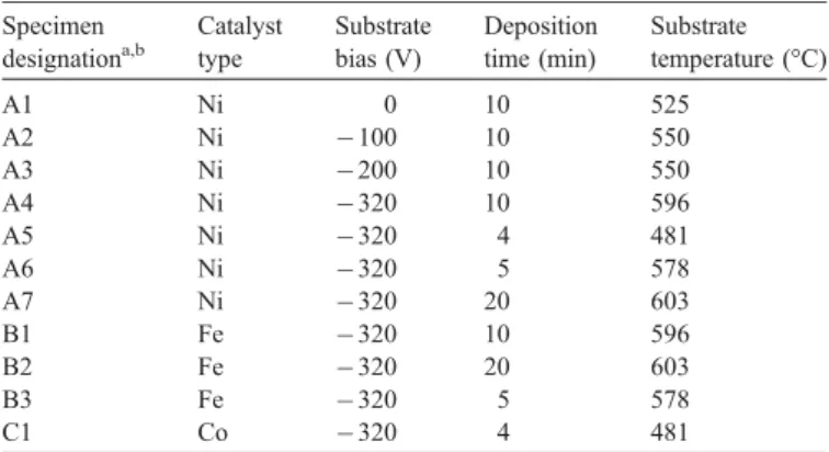
examines no CNTs presenting except amorphous carbon on the substrate surface (Specimen C2). Especially, the CNTs will be extended more into the plasma atmosphere after longer deposition time to suffer greater etching effect. In order to further clarify the deposited nanostructures,Figs. 4(a), (b) and (c) show the HRTEM images of the nanostructures with Ni, Co and Fe as catalysts (Specimens A6, C1, and B3), respectively. These micrographs further support that the nanostructures are all tube-like tip-growth CNTs with catalysts at the tips of the tubes.
3.2. Raman spectra and field emission properties
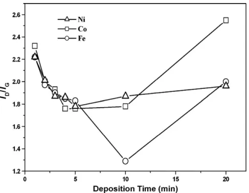
In order to examine the difference in bonding structures of the as-deposited CNTs for different deposition times, Fig. 5
shows three curves of ID/ IG ratio of the Raman peaks as a function of deposition time for CNTs with Fe, Co and Ni as catalysts, respectively. It is interesting to note that there are existences of minimum ratio values (1.29, 1.76 and 1.78, respectively) at the moderate deposition time, which are
corresponding to the best quality of CNTs in the present deposition conditions. By comparing the SEM morphologies with the corresponding ID/ IGratios, it seems to imply that the ID/ IG ratio is a function of sizes, degree of alignment and amorphous carbon contents of the CNTs themselves, and also the surrounding nanostructures after becoming spaghetti-like CNTs. FromFigs. 2(b), (c) and 1(d), which are corresponding to the Ni-assisted CNTs with 5, 10 and 20 min deposition times, respectively, the ID/ IG ratios are about the same (1.8¨1.9). This can be explained by the following reasons: The amorphous carbon contents within CNTs themselves in
Fig. 2(b) are relative higher than inFigs. 1(d) and 2(c), but the exposed amorphous carbons embedded on the nanostructures near the substrate surface are the least. The opposite situation is for Fig. 2(c). The CNTs themselves in Fig. 2(c) with less amorphous carbon contents and sizes are due to the preferential amorphous carbon removal by extending more CNTs into the plasma atmosphere. In contrast, for Fe-assisted CNTs, the SEM morphology in Fig. 3(a) indicates dense bundles of CNTs, which are much smaller in sizes with good quality (Specimen
B1). The most of the exposed nanostructures inFig. 3(b) are basically the etched structures near the substrate surface; therefore reveal a much higher ID/ IGratio (Specimen B2).
The I – V curves and two corresponding Fowler – Nordheim (F – N) plots of the as-grown Ni-assisted CNTs are shown in
Fig. 6 for deposition times ranging from 4 to 20 min (Specimens A4 to A7). It indicates that the CNTs of 10 min deposition time give the best field emission properties (turn-on field = 5 V/Am, field enhancement factor b = 912), though the ID/ IGratios for these four specimens are about the same. The
corresponding nanostructures for the best field emission are shown inFig. 1(d) (Specimen A4), where the CNTs remain in well-aligned manner and are etched to become slightly smaller in sizes, to result in the proper tube number density and higher aspect ratio, and to minimize the screening effect. The nanostructures with the worst field emission are shown in
Fig. 2(c) for deposition time of 20 min (turn-on field is beyond the instrument upper limit, Specimen A7), where the CNTs are the smallest, but scarce and lie down on the nanostructures embedded by amorphous carbons.
Fig. 5. ID/ IGratio of Raman peaks of the as-deposited CNTs as a function of deposition time.
4. Conclusions
A novel process were successfully developed to fabricate the catalyst-assisted CNTs by MPCVD under high negative substrate bias (above 200 V) and pure CH4as the only gas source, but without introducing any additional gas, e.g. H2. The results indicate that the sufficient high negative substrate bias can replace effect of the additional hydrogen source to form various carbon nanostructures. The deposition time can be an important parameter to manipulate the bombardment effect to purify the CNTs structures and to vary the alignment and sizes, so the desired final nanostructures can be obtained. The deposited nanostructures can vary from the well-aligned CNTs of various sizes, the bundles of CNTs, to become the spaghetti-like nanostructures embedded on the amorphous carbon matrix. The well-aligned CNTs with proper tube number densities, purities and sizes can be the best nanostructures to behave excellent field emission properties. Under the present deposi-tion condideposi-tions, the best turn-on field strength can go down to 5 V/Am and the maximum current density at field strength of 10 V/Am is beyond our instrument limit (35 mA/cm2), though there are rooms for much better improvement. On the other hand, the formation of CNTs without additional hydrogen introduction provides the data base to clarify the roles of hydrogen and substrate bias in CNTs growth mechanism.
References
[1] S. Iijima, Nature 354 (1991) 56.
[2] R. Saito, M. Fujita, G. Dresselhaus, M.S. Dresselhaus, Appl. Phys. Lett. 60 (1992) 2204.
[3] M. Yu, O. Lourie, M. Dyer, K. Mooni, T. Kelly, R.S. Ruoff, Science 287 (2000) 637.
[4] S. Fan, M.G. Chapline, N.R. Franklin, T.W. Tombler, A.M. Cassell, H. Dai, Science 283 (1999) 512.
[5] D.S. Bethune, C.H. Klang, M.S. de Vries, G. Gorman, R. Savoy, J. Vazquez, R. Beyers, Nature 363 (1993) 483.
[6] A. Thess, R. Lee, P. Nikolaev, H. Dai, P. Petit, J. Robert, C. Xu, Y.H. Lee, S.G. Kim, A.G. Rinzler, D.T. Colbert, G. Scuseria, D. Tomanek, J.E. Fisher, R.E. Smalley, Science 273 (1996) 483.
[7] L.C. Qin, D. Zhou, A.R. Krauss, D.M. Gruen, Appl. Phys. Lett. 72 (1998) 3437.
[8] C.J. Lee, J. Park, Appl. Phys. Lett. 77 (2000) 3397.
[9] P. Nikolaev, M.J. Bronikowski, R.K. Bradley, Chem. Phys. Lett. 313 (1999) 91.
[10] B. Kitiyanan, W.E. Alvarez, J.H. Harwell, Chem. Phys. Lett. 317 (2000) 497.
[11] C.T. Kuo, C.M. Hsu, C.H. Lin, H.J. Lai, Thin Solid Films 471 (2005) 140. [12] M. Chen, C.M. Chen, C.F. Chen, Thin Solid Films 420 (2002) 230. [13] L. Valentini, I. Armentano, J.M. Kenny, L. Lozzi, S. Santucci, Diamond