Fabrication and characterization of gated Si field emitter arrays with gate aperture below 0.5 im
T. K Ku, B. B. Hsieh, M. S. Chen, C. C. Wang, P. W. Wang, I. J. Hsieh,
and if C. Cheng
Department ofElectronics Engineering and Inst. of Electronics,
National Chiao Tung University,
Department ofElectrical Engineering, Chung-Hua Polytechnic Institute,
Hsinchu, Taiwan, Republic of China.
ABSTRACT
High aspect-ratio single-crystal silicon nücrotips have been fabriCated using the semi-anisotropic dry etching technique.
After the further oxidation sharpening process, arrays of 50X 50 uniformsharp emitter tips has been achieved. The 200 A-thick Cr metal was also coated on the surface of Si microtips to improve the performance. Furthermore, a modified self-aligned process of the gated field emitter arrays (GFETs) has been successfully developed to reduce the fabrication complexity. Employing this method, the tip radius of Si microemitter is about 200 A, and the gate aperture can be easily
reduced to about 0.3 p.m. It will largely decrease the turn-on voltage ofthe field emission devices.
Keywords: oxidation sharpening, microtips, gated field emitter arrays, silicon pedestal, gate aperture, field emission
1. INIRODUCTION
Micrometer-scale vacuum electronics constructedby solid-state fabrication techniques is attracting increasing interest. Potential applications include flat panel displays', ultrahigh-frequency power sources and amplifiers, high..speed logic and
signal processing circuits, and microsensors3. Vacuum microelectronic devices, in fact, have potentially number of
remarkable advantages with respect to the presently much more popular "solid state" counterparts: such as carrier transport
velocity, temperature insensitivity, and radiation hardness. The most fundamental element of field emission device is a
sharp tip used as cold cathode. In our study, the reactive ion etchingtechniques combined with oxidation..sharpening" have been used to form arrays ofuniformly sharp cones on a silicon substrate. The shape ofcones are adjustable depended on the etching process. After the sharp emitter is fonned, a new self-aligned process having more economy steps and flexible has been developed to locate the extraction gate apertures on the ViCinity of the emitter apex. Employing this method, the tip radius of Si microemitter is about 200 A, and the gate aperture can be easily reduced to be about 0.3 jim. This will largely decrease the turn-on voltage ofthe field emission devices5.
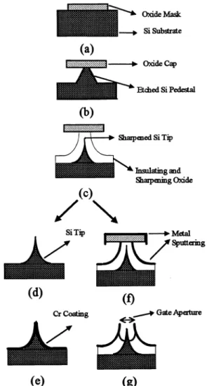
2. FABRICATION PROCESS
2.1 Formation of sharp tip arrays
1im thick oxide layer was thermally grown and was then photolithography patterned to form the arrays of circular
islands with 1 p.tm in diameters. The patterns ofphotoresist wre then transfonned into underlying oxide using anisotropic
reactive ion etching (RIE), as can be seen from Fig. 1 (a). The reactive ion etching od silicon subsequently progressed employing the previously patterned oxide disc as mask. In order to produce the high-aspect-ratio cone-shaped tip, the
parameters used in RIE are the gases flow ratio SFdC12 of 15/45 (sccm/sccm), the RF power of5O W and pressure of about 1.4 mTorr. Theis etchingprocess was terminated earlier to reserve the capped oxide unrelieved on the narrowneck of etched silicon pyramids, as shown in Fig. 1 (b). The width ofthe reserved narrow neck is flexible and typical about 2000—5000 A.
This oxide "capped" silicon pedestal was subsequently exposed to the thermal oxidation ambient. During this process
depicted by Fig. 1 (c), the 1 gm-thick capped oxide mask will serve as an oxidation stopper so that the silicon pedestal was laterally oxidized to form a sharp tip at the pedestal's apex. The sharp Si tips is exposed after stripping the thermal-grown
oxide, as depicted by Fig. 1 (d). Furthermore, some samples of sharpened tip have been overcoated with a 200 A-thick Cr to evaluate the effect of metal-clad Si tips, as indicated in Fig. 1 (e).
2.2 Gate aperture location employing a sell-aligned process
A modified self-aligned process have been successful developed to construct the gated field emitter devices. Referring to Fig. 1 (c), the extraction metal gate is then self-aligned deposited about 2000 A utilizing sputtering depicted by Fig. 1 (f). During
this process, the remaining silicon dioxide caps are not only used to be the lift-off mask but also to be an insulator layer
simultaneously to separate the extraction gate from substrate. The typical thickness ofas-grown oxide insulator is 0.2 0.5
tm
majorly depended on the minimum thickness to sharpen and the desirable gate aperture. Following metal gatedeposition, the underlying oxide exposed on the discontinuity of metal films was then selective removed using buffer HF (BOE) acid, and the metal-clad oxide caps was simultaneously lift offto expose the buried emitter tips. Figure 1 (g) depicts the completed device structure.
3. RESULTS AND DISCUSSION
3.1 Field emitter arrays (YEA's)
Results offormation the sharp silicon tip as FEA's are shown to Fig. 2. The key parameters ofreactive ion etching (RIE) were the choice ofreactive gases. Fig. 2 (a) depicts the high aspect-ratio ('— 4.3 tm/1 j.tm =4.3)oxide-capped silicon pedestal was achievedbythe etchinggases mixture of SFdC12=1/3. The neck ofthe conical silicon pedestal is typical about 1OOO-3OOO A that is determined by etching times. The main problem of RIE etching is the surface roughness caused by
tip-etching process in accordance of the SEM micrograph shown in Fig. 2 (a), but can be smoothed by the following oxidation-sharpening treatment. Figure 2 (b) shows the result after only one 950°Cwet-oxidation-sharpening step. The high resolution SEM micrography shown in Fig. 2 (c) indicate that the as-sharpened tip radius is about 200 A with smooth
morphology. This oxidation-sharpening treatment can repeatedly proceed to further reduce the tip radius to be one nm
range4.
3.2 Gated YEA's for vacuum microtriodes
After the oxidation-sharpening process, the 2500 A-thick-Cr metal is then deposited to be the extraction gate
employing sputtering. Since the metal sputtering is an isotropic and conformal deposition process, the metal gate is uniform deposited on the top of oxide layer except the bottom of overhung oxide caps. To complete the emitter fabrication process, the sample after metal-deposition process was immersedby BOE acid to lift offthe oxide caps and simultaneously removing the underlying oxide to expose the emitter tips. This process results in a high-aspect-ratio volcano-shaped metal gate with a very small gate aperture surrounding the tip apex region. The gate aperture is then controlled by the grown oxide thickness and neck width ofthe original Si pedestal. Since the necks etched by PIE will exhibit the non-uniform width distribution in an array, ensuring that all the tips in an array will be completely sharpened by oxidation-stripping process, the minimum requirement of oxidation thickness is determined by the upper limit in the variation of original neck width. For example, Fig. 1 (a) shows RIE etched tip pedestal with neck width about 23OO 300 A. After the 3000 A-thick-oxide was grown and following the 2500 A-thick-Cr metal deposition, an uniform gated field emitter array(GFEA) with the gate aperture of 0.33 im has been achieved, as shown in Fig. 3 (a). Figure 3 (b) is the cross-section view indicates the tip apex is about 0.33 j.tm recessed to the top plane of gate aperture. Furthermore, Fig. 3 (c) shows that the gate aperture is about 0.26 pin and the tip is nearly at the same level with the top plane of the gate aperture. In both case, the as-fabricated aperture of the
volcano-shaped-gate are much smaller than the original pad oxide size of 1tm. This characteristic is superior than the conventional lift-offtechniques whose gate aperture is limitedby size ofoxide cap7. According to the our previous work in the numerical
simulation5, the more reduced gate aperture means the more increasing in emission current density or the more decreasing the operation voltage at constant current density. Comparing to McGruer et al.6, this new method decreases the process steps by combining the oxidation sharpening and insulator deposition steps. Moreover, this processes need also much fewer steps than the similar work reported by Spallas7, due to using thicker oxide caps instead of complex forming spacers and etching
steps. In addition, the thermally grown oxide shows a better uniformity and breakdown resistibility than the conventional e-gun deposited oxide film.
3.3 Characterization of filed emission from Si and Cr-clad FEAs
The high vacuum measurement environment was set up to characterize the field emission properties. The vacuum
chamber is pumped down by a turbo pump. Cathode contact is made through the holder to the backside of the wafer. The collector (anode) was a copper plate. All cables were shielded except for the ground return path to the power source. The DC
measurement system is based on the Keithley 237 high-voltage source units with IEEE 488 interface. The measurement
instruments are auto-controlledby computer. The schematic diagram ofthe test configuration is shown in Fig. 4. Duringthe measurement, the spacing between the emitter (cathode) and collector (anode) was controlled to be a constant of3Ogm and the base pressure in testing chamber was about 1.O—2.5x10⁷ torr. Prior to the electrical measurement, the emitters were applied with a high constantvoltage ofabout 1 100V to exhaust the adsorbed molecules and evaporate the native oxide. Field emission characterization was obtained from the microtip arrays over a voltage swept from 0 to 1 100V and the tip number
in an array is 50 X 50. Each experimental data point wes extracted by averaging a few tens of measured results.The characteristics of diode current (Id) versus applied voltage (Va) for the FEAS including pure Si, and Si with Cr surface
coating are shown in Fig. 5 (a). The stright slopes in F-N plots shown in Fig. 5 (b) indicated the field-emission
characteristic. At Va=1 100 V, the diode current ofthe pure Si FEA without coating is about 1.41 jtA. It also shows that the Id=19.8 tA for the 200 A-thick Cr-clad Si tips is about 15 times higher than those ofun-coated tips. It is due to the higher electron-supplement capability and the surface electrical conductivity for the Cr ones as compared with Si. Moreover, the thresholdvoltage VT, dfifld as the emission current Id reaches 1 ptA, forpure silicon and Cr-cladare about 1060 V and 855 V, respectively. Thus, the Cr metal surface coating can g,reat improve the field emission capability in comparison with the un-coated Si PEAs.
4. CONCLUSIONS
A new method for fabricating gated field emitter arrays based on the high-aspect-ratio sharp silicon tips have been
successfully developed. The extremely uniform results ofthe volcano-shaped-gate with 0.33 im and 0.26 pm gate aperture have been achieved without the needs ofadvanced lithography process. Such devices can be appliedto serve as low-voltage
vacuum microtriodes. Furthermore, according to the field-emission characterization, the Si PEAs with the thin Cr metal
surface coating can greatly improve the field emission capability in comparison with the un-coated ones.
5. REFERENCES
1. P.Vaudaine and R.Meyer: IEEE. IEDM, p. 197, 1991.
2. C.A.Spindt, C.E.Holland, A.Rosengreen and I.Brodie: J. Vac. Sci. & Technol., B 11, p.s168, 1993. 3. H.H.Busta, J.E.Pogemiller and B.J.Zimmerman, J.Micromech. Microeng., (1993) 45.
4. R. B. Marcus, T. S. Ravi, T. Gmitter, K. Chin, W. J. Orvis, D. it Ciarlo, C. E. Hunt and Trujillo: Appi. Phy. Lett Vol.56, No.3, p.236-238, 1990.
5. T. K. Ku, M. S. Hen, C. C. Wang, M. S. Feng, I. J. Hsieh, C. M. Huang, and H C. Cheng, will publishin Jpn. J. App!. Phy. part. A.
6. N. E. McGruer, K. Warner, P. Singhal, J. J. Gu, and C. Chan: IEEE Trans. on Ele. Dev. Vol.38, No.10, p.2389,
1991.
7. J. P. Spallas, J. H. Das, and N. C. MacDonald J. Vac. Sci. Technol. B Vol.11, No.2, Mar/Apr, p.437-440, 1993.
Oxide Mask
i—+
SiSubrate OxideCap EtthedSi Pedea1(b)
GateApezthreFig. 1 Scheme of new selcaligned fabrication process
Fig. 2 A Si tip array formed by SFdC12 RUE (a)
the etched Si pedestal with remained him-width
oxide caps (b) a sharp Si tip formed after RIE
etching and oxidation-sharpening (c) high
resolution SEM niicrography shows the tip radius
is about 200 A.
SW wv'1r
(a)
SPIE Vol. 2641 I 143(a)
(c)
(d)
(0
(e)
(g)
144 /SP!E Vol. 2641 0 0 0.00001 IE-6 1E-7 IE-8 IE-9 IE-lO ——Cr-clad Si tips LT.A_ Silicontips
S=31pun
IIII.I. I
600 700 800 900 1000 1100Applied Voltage V3(Volt)
(a)
(..G)
Fig. 3 Fabrication results of Si FEAs with the
volcano-shaped-gate (a) a uniform 50x50
GFEA
with a 0.33 .tm gate aperture (b) the cross-section
view ofthe above device indicates that the tips are
about 0.3 .tm recessed to the top plane of gate
aperture (c) another GEFA show a result of only
0.26 itm gate aperture nearly without tip recess.
—11 -12.