Feasibility study of high performance
field emitter pattern with the horizontally
oriented carbon nanotubes by electrophoresis
Chen-Chun Lin
a, Ying-Chun Chen
a, Terry Wang
a, Cheng-Tzu Kuo
b,⁎
a
Department of Materials Science and Engineering, National Chiao Tung University, 1001 University Road, Hsinchu 30010, Taiwan
bDepartment of Materials Science and Engineering, MingDao University, 369 Wen-Hua Road, Peetow, Changhua 52345, Taiwan
a b s t r a c t
a r t i c l e i n f o
Available online 4 September 2008 Keywords:Carbon nanotubes Field emission
For thefield emitter applications, electrophoretic deposition (EPD) followed by post air annealing treatment was developed to selectively deposit the single-walled carbon nanotubes (SWNTs) pattern made of Al and SiO2coatings. The EPD was conducted from a solution mixture of SWNTs and various dispersants or
surfactants, including sodium dodecyl sulfate (SDS), hexadecyl trimethyl ammonium bromide and trictylphosphine oxide. Effects of the processing parameters of EPD and the post air annealing treatment on SWNTs dispersion, morphology,field emission (FE), and film-substrate adhesion were examined. The results indicate that the SDS is the best surfactant in terms of SWNTs dispersion and solution stability, and the EPD parameters have no significant effects on their FE and adhesion properties of the deposited films. However, a higher post annealing temperature combined with an optimum annealing time is required to improve thefilm-substrate adhesion, so to reduce its electrical resistance and to enhance FE properties. The high performance annealedfilms with negligible internal stress are made of the micro-sized islands with the horizontally oriented SWNTs between them. The results also show that the pattern made of conductive and nonconductive coatings, such as Al and SiO2, can be successfully used to deposit SWNTs pattern by EPD.
© 2008 Published by Elsevier B.V.
1. Introduction
Single-walled carbon nanotubes (SWNTs) have many potential applications in nanoscale devices due to their unique structural[1], mechanical [2,3], thermal [4], and electronic properties [5–7]. However, it remains a challenge to uniformly disperse SWNTs for their applications, because as-synthesized SWNTs generally exist as tube bundles or aggregates bound tightly by strong Van der Waals attractions between tubes. There are some methods have been proposed by using both organic and aqueous media as solvents
[8,9], functionizing the tubes[10]and adding surfactants[11,12]. One promising technique being developed for manipulating carbon nanotubes (CNTs) was electrophoretic deposition (EPD) method[13,14]. EPD is achieved via the motion of charged particles dispersed in a suitable solvent, towards an electrode under an applied electricfield. Compared with other processing methods, EPD offers advantages of low costs, process simplicity, uniformity of deposits, well control of deposit thickness, microstructure homogeneity, and deposition on complex shaped substrates, including the potential to infiltrate porous substrates and applicability to a great variety of materials.
In this work, the de-ionized water or butyl alcohol was used as solvent to mix with SWNTs and some surfactants to prepare various
solutions to examine their dispersion ability and stability. The solutions were then adopted to selectively deposit to form the SWNTs patterns for potential applications asfield emitter.
2. Experimental
The raw CNTs in this work consist of bundles of spaghetti-like long SWNTs with average ~ 3 nm in diameter, as examined by transmission electron microscopy (TEM) and Raman spectroscopy, which were prepared by arc discharge method and provided by ITRI (Industrial Technology Research Institute, Taiwan). The typical Raman spectrum of the SWNTs is depicted inFig. 1with strong peaks in radial breathing mode (RBM), indicating existence of SWNTs with high graphitization. There are also two obvious peaks around ~1322 and ~ 1580 cm− 1, which are belong to sp3-bonded (D band) and sp2-bonded (G band) carbon atoms, respectively. The intensity G band to D band ratio can go up to 15.4, also indicating high graphitization.
The SWNT suspensions were made by adding 0.001 g of SWNTs and 0.2 g of the surfactant into 20 mL of solvent (de-ionized water or butyl alcohol) and sonicated for 3 h, where the surfactants (acting as dispersants) include SDS (sodium dodecyl sulfate), CTAB (hexadecyl trimethyl ammonium bromide) and TOPO (trioctylphosphine oxide). The suspension solutions were then centrifuged for approximately 15 min and discarded the sedimentation. The upper supernatant and Al-coated Si wafer were used as the electrolyte and electrodes, respectively, where the gap between electrodes is about 1 cm. Diamond & Related Materials 18 (2009) 520–523
⁎ Corresponding author. Tel.: +886 4 8876660x8050; fax: +886 4 8879050. E-mail address:[email protected](C.-T. Kuo).
0925-9635/$– see front matter © 2008 Published by Elsevier B.V. doi:10.1016/j.diamond.2008.08.002
Contents lists available atScienceDirect
Diamond & Related Materials
Deposition of the dispersed SWNTs on the electrode was conducted by applying dc voltage (10–50 V) for 10–600 s. The SWNTs-coated electrodes were then annealed under air environment on a hot plate at 100–300 °C for 1–15 min. For studying the feasibility of selective deposition technique, the patterns made of Al and SiO2by lithography
process were also used as electrodes.
The stability of suspensions was characterized by UV–visible absorbance spectroscopy and Zeta potential measurements. Struc-tures and properties of the SWNTs or the depositedfilms after each processing step were characterized by field emission scanning electron microscopy (FESEM), high resolution transmission electron microscopy (HRTEM), Raman spectroscopy, energy dispersive spectro-scopy (EDS) andfield emission measurements.
3. Results and discussion
3.1. Effect of the surfactant on stability of CNTs suspension
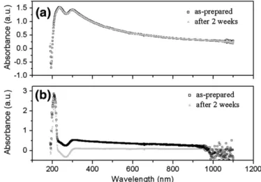
In order to form the deposits with good uniformity in thickness and compositions, it is necessary to prepare suspensions with good stability and well dispersion. The stability of the suspensions was evaluated by UV–visible absorbance spectroscope, basing on depen-dence of absorption to suspension concentration. The results show no significant decreases in absorbance between as-prepared suspension with SDS surfactant and suspension after 2 weeks sedimentation (Fig. 2(a)). In contrast, the suspensions with TOPO or CTAB surfactants indicate significant decrease in absorbance after 2 weeks sedimenta-tion (as also shown inFig. 2(b)). In other words, SDS is a much better surfactant for this application. This may be due to fact that each CNT can be adsorbed by Van der Waals interactions and surrounded by the hydrocarbon hydrophobic part of an anionic SDS surfactant. Then, the sulfate hydrophilic part of the surfactant is oriented towards the aqueous phase, and creates a distribution of negatively charged surface for each surrounded CNT, which prevents their aggregation and induces stable suspensions in water. This suspension stability is also confirmed with the zeta potential measurements, indicating a negativeζ-potential about -60 mV in the pH range from 3 to 11. The zeta potential is an index of the magnitude of the electrostatic interaction between colloidal particles.
The interactions between CNT and SDS surfactant are also consistent with HRTEM and EDS analyses. The suspensions in the solution after ultrasonic agitation are collected by screening and dried in air for HRTEM examination. By comparing the suspensions in the
solutions after 3 h and 15 min ultrasonic agitation, there are more individual SWNT in the former suspension, as shown in Fig. 3(a) HRTEM image, in which some orderly oriented striations are observed on the surface of the CNT, as indicated by an inset. These striations represent the adsorption of the SDS molecules[15]. The corresponding EDS spectrum ofFig. 3(a) is shown inFig. 3(b), where the sulfur peak existence is another evidence for the adsorption of SDS on the surface of the CNTs.
Fig. 1. Raman spectrum of raw SWNTs materials, where the inset is the corresponding detail of RBM spectrum.
Fig. 2. UV–visible absorption spectra of the as-sonicated suspensions and after 2 weeks precipitation for solutions consisting of: (a) SWNTs + SDS + D.I. water, and (b) SWNTs + CTAB + D.I. water, respectively.
Fig. 3. (a) HRTEM image of the SWNT sonicated for 3 h in SDS aqueous suspension (with schematic inset to show the SDS striations), and (b) the corresponding EDS spectrum. 521 C.-C. Lin et al. / Diamond & Related Materials 18 (2009) 520–523
3.2. Morphologies andfield emission properties of the deposited films For EPD conditions of 30 V for 60 s and with SDS as surfactant,
Fig. 4(a) to (c) show the SEM morphologies of the deposited and 3-minute-annealedfilms in air at 3 different annealing temperatures 100 °C, 200 °C and 300 °C, respectively. It shows that a higher post annealing temperature for the depositedfilms gives rise to forming more micrometer-sized islands with the horizontally oriented SWNTs between them (Fig. 4(d)). During progress of annealing, the formation of islands is started by net-like crack forming, crack enlarging, tubes stretching and crack edge curling to release the film stress. Furthermore, it is interesting to note that the horizontally oriented SWNTs across the crack straits, which may provide the opportunity to measure the individual properties of the tubes.
Considering thefield emission (FE) properties of the films,Fig. 5(a) presents the four curves offield emission current density (J) versus electric field (E) for the annealed films at different annealing temperatures, respectively. The results indicate that the EPD para-meters, i.e. the applied voltage, electrode distance or deposition time, have no significant effects on its FE properties. In contrast, the post annealing temperature and time have a notable influence on their FE properties. The annealing process is purposed to enhance the possible chemical bonding between thefilm and the Al substrate, and also to remove some volatile materials and solvents in thefilms. The turn-on field (Eto), which is defined as the electric field required to produce an
emission current density of 0.01 mA/cm2, decreases with increasing annealing temperature, showing Etodown to ~2.4 V/μm at the highest
annealing temperature of 300 °C inFig. 5(a). According to FE study, the emission sites of CNTs are mainly from the defected areas of the walls or bodies of tubes[16–19]. At higher annealing temperature, there are more horizontally oriented clean SWNTs stretched between the cracked islands, as shown inFig. 4, which may provide more favor emission sites to enhance the FE properties. At 300 °C annealing temperature,Fig. 5(b) show the J–E curves as a function of annealing
Fig. 4. SEM micrographs of the deposited and 3-minute-annealedfilms on Al-coated Si substrate under same EPD deposition conditions but different post annealing temperatures: (a) 100 °C, (b) 200 °C and (c) 300 °C, respectively. The corresponding image of (c) at higher magnification is shown in (d).
Fig. 5. J–E curves of the deposited and annealed films on Al-coated Si substrate: (a) under same annealing time (5 min) but different annealing temperatures, respectively, and (b) under same annealing temperature (300 °C) but different annealing times, respectively. 522 C.-C. Lin et al. / Diamond & Related Materials 18 (2009) 520–523
time. There is an optimum annealing time (~ 5 min) to obtain the best FE properties. In order to examine the possible reasons for the best FE properties, the tape-pulling and scratching tests were adopted to study the adhesion of the depositedfilms after post annealing. This is based on the fact that a poorfilm-substrate adhesion generally results in greaterfilm-substrate electrical resistance and so poorer emission ability. When the annealing time is longer than 10 min, the edges of the islands will become curling and the curling edges can cause poor adhesion and worse FE properties. In other words, a higher annealing temperature and a proper annealing time are essential to obtain the bestfield emission properties, where the film-substrate adhesion may play an important role.
3.3. Deposition selectivity of the EPD process
The patterns made of the Al-coating and SiO2films were used as
substrate to examine the deposition selectivity of the SWNTs by EPD. Under EPD conditions of 30 V for 60 s and post annealing of 300 °C for 5 min, the SEM morphologies of the depositedfilms at the Al/SiO2
interface and on the Al coating part of the Al–SiO2pattern are shown
inFig. 6(a) and (b), respectively. It is obvious that at the left side of
Fig. 6(a), or the nonconductive SiO2region of the pattern, there are no
detectable SWNTsfilms on the surface. In contrast, there are denser of the SWNTs islands on the conductive Al regions of the pattern, as shown inFig. 6(b) and right side ofFig. 6(a), indicating an excellent selectivity of the EPD for the SWNTs pattern deposition.
4. Conclusions
In this work, the EPD with SDS surfactant followed by post annealing treatment was successfully developed to deposit the SWNTs pattern made of conductive and nonconductive materials, such as Al and SiO2 coatings. For the field emission display applications, the
results show that the most important parameters of the EPD and post
annealing treatment are surfactant material, post annealing tempera-ture and time. The SDS surfactant is the best choice in this case. A higher post annealing temperature under an optimum annealing time is more favor for the best FE properties (Eto~ 2.4 V/μm). The results also
show that the best FE properties of thefilms are often the films with the bestfilm-substrate adhesion strength.
Acknowledgements
This work was supported by the National Science Council of Taiwan, under Contract No. NSC96-2221-E-451-012.
References
[1] S. Iijima, Nature 354 (1991) 56.
[2] M.F. Yu, O. Lourie, M.J. Dyer, K. Moloni, T.F. Kelly, R.S. Ruoff, Science 287 (2000) 637. [3] M.M.J. Treacy, T.W. Ebbesen, J.M. Gibson, Nature 381 (1996) 678.
[4] S. Berber, Y.K. Kwon, D. Tománek, Phys. Rev. Lett. 84 (2000) 4613. [5] N. Hamada, S. Sawada, A. Oshiyama, Phys. Rev. Lett. 68 (1992) 1579.
[6] R. Saito, M. Fujita, G. Dresselhaus, M.S. Dresselhaus, Appl. Phys. Lett. 60 (1992) 2204.
[7] W.A. Deheer, A. Chatelain, D. Ugarte, Science 270 (1995) 1179.
[8] J. Hilding, E.A. Grulke, Z.G. Zhang, F. Lockwood, J. Disper. Sci. Technol. 24 (2003) 1. [9] C.S. Du, J. Yeh, N. Pan, J. Mater. Chem. 15 (2005) 548.
[10] D.H. Marsh, G.A. Rance, M.H. Zaka, R.J. Whitby, A.N. Khlobystov, Phys. Chem. Chem. Phys. 9 (2007) 5490.
[11] M.F. Islam, E. Rojas, D.M. Bergey, A.T. Johnson, A.G. Yodh, Nano Lett. 3 (2003) 269. [12] Y. Kim, S. Hong, S. Jung, M.S. Strano, J. Choi, S. Baik, J. Phys. Chem. B 110 (2006) 1541. [13] A.R. Boccaccini, J. Cho, J.A. Roether, B.J.C. Thomas, E.J. Minay, M.S.P. Shaffer, Carbon
44 (2006) 3149.
[14] S.L. Quale, J.B. Talbot, J. Electrochem. Soc. 154 (2007) K25.
[15] C. Richard, F. Balavoine, P. Schultz, T.W. Ebbesen, C. Mioskowski, Science 300 (2003) 775.
[16] Y. Chen, D.T. Shaw, L. Guo, Appl. Phys. Lett. 76 (2000) 2469.
[17] C.M. Hsu, C.H. Lin, H.L. Chang, C.T. Kuo, Diamond Relat. Mater. 420–421 (2002) 225. [18] G. Zhou, W. Duan, B. Gu, Appl. Phys. Lett. 79 (2001) 836.
[19] Y.S. Jung, D.Y. Jeon, Appl. Surf. Sci. 193 (2002) 129.
Fig. 6. The SEM morphologies of the EPD-prepared SWNTs pattern made of Al and SiO2coatings: (a) at Al/SiO2interface (with schematic inset to show the interface position on the
pattern), and (b) on the Al region of the pattern.
523 C.-C. Lin et al. / Diamond & Related Materials 18 (2009) 520–523