國 立 交 通 大 學
電子工程學系 電子研究所碩士班
碩 士 論 文
電偶極工程與高介電係數阻絕層於氮化矽與奈米微
晶粒非揮發性記憶體之研究
A Study of the Impact of Dipole Engineering and
High-k Blocking Layer on Nonvolatile Memories
with Nitride and Nanocrystal Trapping Layer
研 究 生 : 陳國永
指導教授 : 簡昭欣 教授
電偶極工程與高介電係數阻絕層於氮化矽與奈米微晶粒
非揮發性記憶體之研究
A Study of the Impact of Dipole Engineering and High-k
Blocking Layer on Nonvolatile Memories with
Nitride and Nanocrystal Trapping Layer
研 究 生 : 陳國永 Student : Kuo-Yung Chen
指導教授 : 簡昭欣 教授 Advisor : Dr. Chao-Hsin Chien
國 立 交 通 大 學
電子工程學系 電子研究所碩士班
A thesis
Submitted to Department of Electronics Engineering
and Institute of Electronics
College of Electrical and Computer Engineering
National Chiao Tung University
In Partial Fulfillment of the Requirement
For the Degree of Master
in
Electronic Engineering
August 2010
Hsinchu, Taiwan, Republic of China
電偶極工程與高介電係數阻絕層於氮化矽與奈米微晶粒
非揮發性記憶體之研究
學生: 陳 國 永 指導教授: 簡 昭 欣 教授
國立交通大學
電子工程學系 電子研究所碩士班
摘 要
在本論文中,我們先利用多晶矽-氧化矽-氮化矽-氧化矽-單晶矽型式(SONOS-type) 的電容平帶電壓變化,探討氧化鋁(Al2O3)與二氧化鉿(HfO2)在二氧化矽(SiO2)的接面上產生的"本質電偶極"(intrinsic dipole)。我們發現當氧化鋁或二氧化鉿沉積在二氧化矽 上會使電容的平帶電壓變大,反之若是二氧化矽沉積在氧化鋁或二氧化鉿會使其平帶電 壓變小。我們也發現氧化鋁產生的本質電偶極大約是二氧化鉿的兩倍。接下來將這個結 果運用在二氧化鉿的奈米結晶粒的非揮發性快閃記憶體元件,發現元件的電容平帶帶壓 變化有相同的結果,但由於此次實驗元件有很嚴重的閘極注入電子,使元件在福勒-諾 德漢穿隧(Fowler Nordheim tunneling)抹除操作時無法正常運作,但接下來的實驗中我們 將解決此問題。
再者,我們利用了高介電係數材料(Al2O3,HfAlOx)取代二氧化矽當作阻絕氧化層運
電常數材料並不會因會我們的離子佈值後退火產生嚴重的劣化。我們驗證介電係數越高 的阻絕氧化層材料記憶體操作速度亦越快,但由於此高介電係數材料中的缺陷,使我們 在抹除操作時有暫態的現象。此元件擁有很快的寫入速度(programmin speed),同時也有 很高的資料保持度(retention),在經過一萬次的寫入抹除操作下(endurance)依然可以維持 很好的記憶體效果。 最後,我們結合了之前的分析,將本質電偶極(Al2O3, HfO2)沉積在穿隧氧化層上, 且運用高介電係數材料(Al2O3)的阻絕氧化層,做出多晶矽-氧化鋁-氮化矽-氧化矽-單晶 矽型式的非揮發性記憶體元件。我們發現元件的臨界電壓會因電偶層存在而變大。我們 分別利用福勒-諾德漢穿隧(Fowler Nordheim tunneling)與熱載子注入(hot carrier injection) 兩種操作方式探討此電偶層對於元件的寫入與抹除的情況,並且探討其資料保(retention) 度與元件的容忍度(endurance)和擾亂程度(disturbance)的影響。
A Study of the Impact of Dipole Engineering and High-k
Blocking Layer on Nonvolatile Memories with
Nitride and Nanocrystal Trapping Layer
Student: Kuo-Yung Chen Advisor: Dr. Chao-Hsin Chien
Department of Electronics &
Institute of Electronics
National Chiao Tung University
ABSTRACT
In this thesis, we first study the influence of the presence of “intrinsic dipole” on the electrical properties of a SONOS-type nonvolatile memory (NVM) by a capacitor structure. The magnitudes of “intrinsic dipole” were extracted by the VFB shift observed in the C-V
curves of the capacitors with adding Al2O3 or HfO2 inside the standard gate stack structure of
a SONOS-type NVM, i.e., SiO2/Si3N4/SiO2. We found that VFB shifted toward positive
direction when Al2O3 or HfO2 were deposited on top of SiO2 (tunneling layer). In contrast,
VFB shifted toward negative direction when Al2O3 or HfO2 was deposited on top of Si3N4
(blocking layer). In addition, the magnitude of VFB shift for Al2O3 was about twice larger than
HfO2. Next we also applied this scheme to the HfO2 nanocrystal SONOS-type NVM, and
conventional SONOS NVM. However, there was a serious gate injection problem in our device, so the fabricated devices can not be normally erased by FN-tunneling. We would tackle this problem in later chapters.
Then, we adopted the high-k material (Al2O3, HfAlOx) to replace the traditional SiO2 as
blocking layer for the HfO2 nanocrystal NVM. With high thermal budget processing for
device fabrication, the high-k materials sustained pretty well and did not depict visible degradation. We exhibited the HfAlOx as blocking layer having faster programming and
erasing speed. However, there were plentiful defects in the HfAlOx layer, and this made our
device have “transient phenomenon” during erase operation. For our nanocrystal memory devices, there were advantages of fast programming speed, excellent data retention time at room temperature, and superior endurance after P/E cycles of 104.
Finally, we adopted the intrinsic dipole scheme, i.e., depositing additional Al2O3 and
HfO2 on top of tunneling oxide and used Al2O3 as blocking layer to make the so called
SANOS-type NVM. The presence of dipole reflected on the observed larger device threshold voltage than the conventional one. Here we use both the FN-tunneling and hot carrier injection to study the electrical characteristics of the fabricated devices. We found that FN-tunneling operation has led to better endurance than hot carrier injection operation. Moreover, we also discussed the impact of dipole engineering on the retention and disturbance characteristics of our newly-developed nonvolatile memories.
誌 謝
在碩士的求學過程中,首先要感謝的是指導教授 簡昭欣博士,感謝老師在兩年前 讓我加入實驗室,使我在求學過程中成長不少。研究上老師嚴謹的態度與博學的知識令 人欽佩,對於生活上老師和藹的待人模式以及豁達人生觀也是我值得學習的地方,此外 老師也提供了我們很好的學習環境,我們的實驗室裝潢大概是數一數二舒服的吧!哈哈! 真的很開心能夠加入老師帶領的實驗室。 接下來就是要感謝實驗室的各位學長,同學以及學弟們。振華學長,感謝你對我問 題上的指導以及關心。豪育學長,有問題向你請教時,你也都會很耐心的為我們解答, 謝謝學長。明瑞學長,感謝學長在旺宏的計畫時給我很多指導與幫助,學長在我們升碩 二時就回宜蘭了真是太可惜拉!志彥學長,真的很感謝學長實驗上給我的幫助,如果沒 有學長我大概實驗會有很多問題不能解決吧,謝謝學長常常抽出時間幫助我。兆欽學 長,學長很多精神真的很值得我學習,有時候看你很晚的時候都還會準備資料,真的是 很能夠讓我們激勵而且有問題時你也都會為我們解答。家豪學長,學長常常給我元件跟 製程上的寶貴建議,讓我對元件觀念更清楚,也都會耐心的跟我討論,告訴我很多方法 讓我處理事情更有效率,真是謝謝學長阿!宗元學長,後來很多量測時有問題都會向你 請教,真的很感謝!宇彥學長,學長的求學知識與實驗精神很值得我學習唷!胖哥學長, 感謝胖哥給我很多實驗與元件的觀念,一開始很多實驗都靠你教,跟你討論的時候也常 能讓我對記憶體更加認識,哈!希望你順利的達成理想唷!政庭學長,常常元件有問題都 是問你,讓我了解不少,果然是資格考輕鬆過關的人,實驗上也對我幫助很大,好險後 來跑新廠的時候實驗室還有你可以問,呼~!宗佑學長,實驗室的大掌櫃,meeting 的時 候都可以問出問題讓老師也覺得問得很好,厲害唷,實驗室三五族靠你啦!小朱學長, 我記憶體的東西都靠你跟胖哥幫我了,不管是實驗上還是任何觀念,一開始學機台也是 你細心指導我,除了感謝還是感謝阿!耀陞學長,我們一起打壘球的壘球場變成回憶了, 被蓋大樓了啦@@!還記得我剛進來你就找我丟壘球,真開心阿!大鳥學長,實驗室笑點都靠你跟胖哥啦!常常聽到你跟胖哥互嗆棒球,我真的在旁邊笑的很開心。 再來是實驗室的同學與學弟們。吳博學長!?同學!?呵!一開始碩一都吳博吳博的叫! 果然現在變學長了,希望你資格考順利,等你們大家請客阿,哈哈!禎晏,元件觀念很 清楚,碩一跟碩二有問題都會問你,讓我有不同的思考方向,果然是電資學士班的學生 阿!宗霖,呵!還記得大四常常在圖書館同樓層唸書吧,那時候還不是很熟,沒想到後來 變同學摟!恭喜我們都考到理想的研所還進入到好實驗室阿。瑞國,加油阿!希望你實驗 順利啦,太陽能產業靠你啦!昶智,同樣是機電系大學的學弟,機電系靠你發揚光大了, 話說我好懷念大學阿!加油!韋志,做實驗不要緊張阿!元件這麼早跑出來,又有政庭帶 你安啦,加油!哈!姿慧,實驗室的唯一女生!也是電資學士班的強者,加油! 再來感謝 NDL 很多人的幫忙,耘木 疌、琇芝姐、李姐、家如姐、子綾姐、婉 貞 姐 、 明 娟 姐 、范姐、鳳 姐 、蔣姐, 感 謝 各 位 美 女 的 幫 忙 與 支 持 !讓 我 在 實 驗 時 很 順 利 的 進 行 , 哈 哈 !還 有 感 謝 宋 爺 run card 的 協 助 。 感 謝 張 國 明 老 師 實 驗 室 的 很 多 學 生,淫 蟲,以我們的交情!應該不用多說太多 吧,哈哈!煒力、老古、阿嘉學長、學威、俊傑、偉強、政勳,沒有你們我大概少了很 多快樂的時光吧!還有最瘋狂的冠名!呵!我們應該也是不用多說的吧! 接下來要當然是要感謝最重要的爸爸媽媽,謝謝爸媽提供我無憂無慮的學習環境, 從小沒有給我什麼壓力,開明的教導方式讓我很自主的可以決定我的所學,即使我有什 麼需求也都會支持我!謝謝爸媽辛苦的工作我才有這樣的成長環境!大姐跟姐夫,哈!讓 我有一個這麼可愛的侄子真是開心阿!大姐從小算是我的好榜樣吧,又很關心我,姐夫 人也是好得沒話說阿。二姐,很疼我也很關心我,從小很多事情都靠姐姐幫我,常常都 會送我很好的禮物!哈哈!感謝上天給了我一個這麼好的家庭!我會好好努力的!謝謝我 的女友,陪我度過了考研究所的艱難時期,還有碩士班的生涯很多時間也都是靠你陪 我,我們有好多好多快樂時光!希望你也快點考上會計師喔! 感謝以上的人,讓我能順利完成碩士論文,總之跟我認識的人都很感謝!謝謝大家! 接下來要去保衛國家了!加油!
Contents
Abstract (Chinese) ………....I Abstract (English) …..………III Acknowledge……….V Contents ...….………VII Figure Captions ………...X Table Lists ………..………..XVI
Chapter 1 Introduction………..1
1.1 Overview of Nonvolatile Memory ………...1
1.2 Motivation ………5
1.3 Organization of the Thesis ………...6
Reference ……….………7
Chapter 2 Effect of Interfacial Dipole on SONOS-type Memory Capacitors and Nanocrystals Memory Devices……….15
2.1 Introduction ………15
2.2 Experiment ……….16
2.3 Results and Discussion ………...……17
2.3.1 Effect of Interfacial Dipole on SONOS-type Capacitor ………...17
2.3.2 Effect of Interfacial Dipole on Nanocrystal Memory Device ………...19
2.4 Summary ………19
Chapter 3 Characteristic of HfO2 Nanocrystals Nonvolatile Flash Memory with High-k
Blocking Layer ……….39
3.1 Introduction ………39
3.2 Experiment ……….40
3.3 Results and Discussion ………...40
3.3.1 Material Analysis of Al2O3 and HfAlOx Blocking Layer ………..40
3.3.2 Characteristics of Program/Erase Operation ……….42
3.3.3 Transient Phenomenon of Erasing Operation ………...…42
3.3.4 Data Retention ………...43
3.3.5 Endurance ………...……….………..44
3.4 Summary ………44
Reference ……….……..45
Chapter 4 SANOS Nonvolatile Memory Devices with Dipole Layer Engineering ...…64
4.1 Introduction ..………..64
4.2Experiment ……….……….64
4.3 Results and Discussion ………...65
4.3.1 Characteristics of Program/Erase Operation ……….65
4.3.2 Retention ………...67
4.3.3 Endurance ……….…….68
4.3.4 Disturbance ………...………68
4.4 Summary ………...……….69
Reference ……….……..70
Chapter 5 Conclusions and Further Recommendations ....………86
5.2 Further Recommendations ……….………87
Figure Captions
Chapter 1
Fig 1.1 (a) Schematic of a basic conventional SONOS Flash memory device. (b) Vertical migration of stored charge in Si3N4 trapping and lateral migration of the stored in the
HfO2 trapping layer in SONOS memory device structure.
Fig 1.2 (a) Schematic of a basic BE-SONOS [10] Flash memory device. (b) The band structure of BE-SONOS tunneling layer at low electric field during retention and hole tunneling erase at high electric field due to the band offset.
Fig 1.3 (a) An illustration if a nanocrystal memory. (b) The nanocrystal can store the charge locally due to the well isolation of nanocrystal from each other and effectively prevents formation of good conductive paths between the adjacent nodes.
Fig 1.4 (a) Schematic of a basic TANOS [17] Flash memory device. (b) The band diagram compare with SiO2 and Al2O3 as blocking oxide during erase situation. The Al2O3
can effectively inhibit gate injection than SiO2.
Fig 1.5 (a) The principle of CHE program. (b)The band diagram of use band to band hot hole injection erase. (c) The band diagram of use Fowler-Nordheim tunneling to program.(d) The band diagram of use Fowler-Nordheim tunneling to program.
Fig 1.6 Current-Voltage characteristics of a memory device in the programmed state and erase state display the VT shift and memory window.
Chapter 2
Fig. 2.1 (a) Relationship between EWF of metal gate along with n+poly-Si on high-k and SiO2. (b)Schematic band diagram of Al2O3/SiO2, HfO2/SiO2, and Y2O3/SiO2 systems
[2.8]. (c) Summary of the dipole moment formed at High-k/SiO2 interface predicted
by [2.12].
Fig 2.2 Schematic of conventional SONOS memory capacitors with interfacial dipole layer engineering.
Fig 2.3 Schematic of HfO2 nanocrystal flash memory structure with interfacial dipole layer
engineering
Fig 2.4 (a) Cross-sectional TEM image of Si/SiO2/Al2O3/Si3N4/SiO2. The ultra-thin Al2O3
layer is well formed upon the bottom SiO2. (b) Cross-sectional TEM image of
Si/SiO2/Al2O3/Si3N4/Al2O3/SiO2. The ultra-thin Al2O3 layer is well formed upon the
bottom SiO2 and Si3N4.
Fig 2.5 (a) Schematic of capacitor structure of discussion the influence of the dipole deposit between bottom oxide and nitride trapping layer and (b) their C-V characteristics with Al2O3 5 Å, 10 Å, 20 Å, 30 Å, HfO2, 10 Å, and 20 Å.
Fig 2.6 (a) The result of VFB shift with interfacial deposit on bottom oxide in Figure 2.5(b). (b)
The band diagram of SONOS-type capacitor with interfacial deposit on bottom oxide.
Fig 2.7 (a) Schematic of capacitor structure of discussion the influence of the dipole deposit on nitride trapping layer and (b) their C-V characteristics with Al2O3 10 Å and HfO2
10 Å.
Fig 2.8 (a) Schematic of capacitor structure of discussion the influence of the dipole deposition between nitride layer and top oxide and (b) their C-V characteristics with Al2O3 10 Å, 20 Å, and 30 Å.
Fig 2.9 (a) The result of VFB shift with interfacial deposit on nitride layer in Figure 2.8(b). (b)
The band diagram of SONOS-type capacitor with interfacial deposit on nitride layer. Fig 2.10 (a) Schematic of capacitor structure of discussion the influence of the double dipole
with Al2O3 10 Å, 20 Å,30 Å, HfO2,10 Å , and 30 Å on nitride layer.
Fig 2.11 The band diagram of SONOS-type capacitor with interfacial deposit on bottom oxide and on nitride layer.
Fig 2.12 IDS-VGS curve of the nanocrystal flash memory with Al2O3 dipole layer engineering
Fig 2.13 Plots of ICP vs VGBLl for the HfO2 nanocrystal memory cell with different frequency
and the parameter after calculate.
Fig 2.14 (a) IDS-VGS curve of the nanocrystal flash memory with programming time 1s and
erasing time 1s. (b)The band diagram of nanocrystal memory at erasing operation and have seriously gate injection.
Fig 2.15 (a) Retention characteristics of nanocrystal flash memory at room temperature (T=25℃) with 104 second. (b) The band diagram of retention. The losing charge is mainly escape by blocking oxide not tunneling oxide.
Fig 2.16 C-V characteristics of our nanocrystal and nanocrysta with dipole layer engineering flash memory..
Chapter 3
Fig 3.1 (a) The band diagram of SONOS-type memory with different primitive but equal bandgap material as blocking layer at negative gate voltage. (b) The band diagram of SONOS-type memory with Al2O3 and HfO2 as blocking layer at negative gate
voltage.
Fig 3.2 Schematic of MOS capacitors with Al2O3 and HfAlOx.
Fig 3.3 Schematic of HfO2 nanocrystal flash memory structure with Al2O3 and HfAlOx as
blocking layer.
Fig 3.4 (a) The MOS capacitor Current Density-Electric Field (J-E) characteristics of Al2O3
Fig 3.5 (a) The MOS capacitor C-V hysteresis characteristics of Al2O3 without PDA and (b)
with PDA of 950℃ 30s embedded N2. (c) The MOS capacitor C-V hysteresis
characteristics of HfAlOx without PDA and (d) with PDA of 950℃ 30s embedded
N2.
Fig 3.6 The analysis of XPS of HAlOx film with pulse ratio Al: Hf= 3: 1 which contain the
Intensity-Binding Energy characteristic of Al, Hf, and O.
Fig 3.7 The analysis of XRD of (a) Al2O3, (f) HfO2, and (b), (c), (e), (d), HfAlOx after 950℃
30 second PDA treatment.
Fig 3.8 IDS-VGS curve of the nanocrystal flash memory with HfAlOx as blocking layer.
Fig 3.9 IDS-VGS curve of initial state, programming state with VG=16V 1us and erasing state
with VG=-16V 10ms.
Fig 3.10 Programming characteristic of our nanocrystal memory as a function pulse width for different FN-tunneling operation condition.
Fig 3.11 Erasing characteristic of our nanocrystal memory as a function pulse width for different FN-tunneling operation condition
Fig 3.12 IDS-VGS curve of initial state, programming state with VG=16V 1us and erasing state
with VG=-16V 100ms and (b) 1ms to discuss the transient phenomenon.
Fig 3.13 (a), (b) and (c) The reason of the transient phenomenon for our speculation. (a) After the program pulse. (b)After erase pulse. (c) After Sweep IDS-VGS to detect erasing
state.
Fig 3.14 (a) Retention characteristics of our nanocrystal flash memory with Al2O3 and (b)
HfAlOx as blocking layer at room temperature (T=25℃). (c) Retention
characteristics of our nanocrystal flash memory with Al2O3 and HfAlOx as blocking
layer at room temperature (T=25℃) with normalized VT Shift.
Fig 3.15 Retention characteristics of our nanocrystal flash memory with Al2O3 and (b)
Shift.
Fig 3.16 (a) and (b) Schematic of endurance characteristics of our nanocrystal flash memory with HfAlOx and (c) Al2O3 with different operation condition. (c) Schematic of
endurance characteristics with Al2O3 is under different operation condition.
Chapter 4
Fig 4.1 Schematic of SANOS of dipole engineering flash memory structure with Al2O3
blocking layer.
Fig 4.2 (a) IDS-VGS of our SANOS flash memory with different operation voltage of
W/L=0.35 μm/1μm and (b)W/L= 10μm/1μm, and shows excellent characteristics compare with the previous chapters.
Fig 4.3 IDS-VGS curve of SANOS and dipole layer engineering SANOS memory..
Fig 4.4 (a) IDS-VGS curve of initial state, programming state with FN tunneling at VG=14 1ms
and erasing state with FN tunneling at VG=-16V 10ms of our conventional SANOS
device. (b) IDS-VGS curve of initial state, programming state with CHE operation at
VG=8V and VD=8V 5ms, and erasing state with BTBHHI operation at VG=-7V and
VD=9V 10ms of our conventional SANOS device.
Fig 4.5 (a) Programming characteristic as a function of pulse width for different FN-tunneling operation condition. (b) We try to give the same voltage to make up the different VT
due to the dipole layer.
Fig 4.6 Using a dipole layer is expected to result in easier programming at a given tunnel oxide electric field [4.2].
Fig 4.7 Erasing characteristic as a function of various FN-tunneling operation conditions. Fig 4.8 Dipole layer incorporation causes a slightly slower erase at a given tunneling oxide
[4.2].
Fig 4.9 Programming characteristic as a function of pulse width for different CHE operation condition.
Fig 4.10 Erasing characteristic as a function of pulse width for different BTBBHI operation condition.
Fig 4.11 Retention characteristics of our SANOS flash memory and SANOS with HfO2 and
Al2O3 dipole layer engineering at room temperature (T=25℃).
Fig 4.12 Data retention characteristics of normalized VT shift at room temperature (T=25℃),
the result follows the trend: SANOS-Al2O3 > SANOS-HfO2 > SANOS.
Fig 4.13The band diagram of SANOS devices with dipole layer engineering during retention [4.2].
Fig 4.15 Schematic of endurance characteristics of SANOS and SANOS-type memory with dipole layer engineering with FN-tunneling operation.
Fig 4.16 Schematic of endurance characteristics of SANOS and SANOS-type memory with dipole layer engineering with hot carrier injection operation.
Fig4.17 NOR array circuit for nonvolatile memory.
Fig 4.18 Gate disturbance characteristics of SANOS and SANOS-type memory with dipole layer engineering in the erasing state.
Fig 4.19 Drain disturbance characteristics of SANOS and SANOS-type memory with dipole layer engineering in the erasing state.
Fig 4.20 Read disturbance characteristics of SANOS and SANOS-type memory with dipole layer engineering in the erasing state.
Table Lists
Chapter 3
Table 3-1 After calculation, we can obtain the composition ratio of Al: Hf with different pulse ratio off Al: Hf = 7: 1 , 3:1, 1:1, and 5:1 in this table.
Chapter 1
Introduction
1.1 Overview of Nonvolatile Memory
The semiconductor industry have made progress continuously with complementary metal-oxide-semiconductor (CMOS) memory technology, thus people’s life have been changed by various kinds of portable electronic products ,such as cell phone, MP3 player, digital camera, notebook computer, and other personal electronic consumed products whatever you can think. It’s apparent to represent memory device, which playing the important role in our life.
It’s simple to distinguish memories intotwo main categories by whether the stored data will vanish or not with power supply. If they lose stored information once power supply is switch off and it’s called volatile memory, such as DRAM. Otherwise, it is Nonvolatile Memory (NVM) such as ROM. About NVM it let we can stored our picture in our digital camera and store music in MP3 player. Because it keep stored information also when the power is switch off.
With the NVM device continuously developed, we can also divide NVM into non-charge-based memory like MRAM [1.1], RAM [1.2] and charge-based memory like Intel ETOX [1.3].The typical charge-based memory is also called flash memory. As the different trapping layer, there are three types of flash memory including the floating gate (FG) type, SONOS [1.4] (Silicon/Oxide/Nitride/Oxide/Silicon) type, and nano-crystal [1.5] or metal-dot type. Among the types of memories mentioned about, flash memory has the advantage of good program/erase (P/E), low operation, small area ,low power consumption, and low cost. In 1967,D Kahng and S. M. Sze invented the first floating-gate(FG) nonvolatile
semiconductor memory at Bell Labs[1.6]. These days, a lot of electronic products still adopt the floating-gate structure. Nevertheless, the current floating-gate flash faces a critical scaling challenge due to the floating gate coupling effect [1.7].
The tunnel oxide of floating gate device has to be thick enough (8~10nm) to maintain superior retention and endurance, but it also cause large operation voltage, high power consumption, slow program/erase (P/E) speed, and the most important, hard to be scaled. In addition to, the poly silicon floating-gate is conductive; the total charges stored in floating gate would be easily lost when the tunnel oxide has a single defect or damaged during P/E cycles, such as SILC issues [1.8]. On the other word, the scaling limit of floating-gate memory to lateral and vertical is charge loses due to SILC and the effect of parasitic capacitive coupling. Moreover, the trapping layer is conductive, so it can’t use Multi-Level Cell (MLC) to make data with double density. To overcome these disadvantages mentioned above, new memory structure, such as SONOS type, and nano-crystal or metal-dot type memory, will be the solution to these problems.
SONOS-type (Silicon/Oxide/Nitride/Oxide/Silicon) devices are forecasted as the solution beyond the 45-nm node [1.9] because charge trapping devices are naturally immune to the floating gate coupling interference. The conventional SONOS memory is shown in
Figure 1.1(a). It has recently been a promising candidate for the next-generation nonvolatile
memory. Contrary to the floating gate device where charge is uniformly stored in the floating gate, the charge is locally trapped in the nitride thin film. It can avoid to SILC issues, coupling effect, and not only SLC (single level cell) operation. However, conventional SONOS memory still has some problems, such as electron vertical and lateral migration show in Figure 1.1(b) and data retention. Next we did some discussion to see others people how to improve. There are three points of SONOS-type flash memory with O/N/O structure that we can discuss which were tunneling layer, trapping layer, and blocking layer.
The fist” O” is SiO2 as tunneling oxide (bottom oxide) with normal SONOS-type device.
In 2005 the MXIC use the ultra-thin “ONO” (Oxide/Nitride/Oxide) to replace the tunneling oxide and it named to BE-SONOS (Bandgap-Engineered SONOS) [1.10]. The structure is shown in Figure 1.2(a). The ultra-thin ONO layer provide a modulated tunneling barrier, it reduces direct tunneling at low electric field during retention, but it allows efficient hole tunneling erase at high electric field due to the band offset. The band structure is shown in
Figure 1.2(b) .Therefore, this BE-SONOS offers fast hole tunneling erase, while it is immune
to the retention problem of the conventional SONOS. And the ultra thin ONO layer is trap free and use the simple material, which may improve the reliability issues with conventional SONOS.
Trapping layer
The “N” is Si3N4 as trapping layer with normal SONOS-type device. In recent years, the
trapping layer materials have been investigated to improve the cell data retention. For example, the use of an Al2O3 trapping layer and HfAlOx to replace Si3N4 have been consider
since their material band gaps and high trap densities offer superior program/erase speed and data retention [1.11]. Moreover, various kinds of nanocrystal, such as silicon (Si) [1.12], germanium (Ge) [1.13], and metal nanocrystal, may be use to provide charge storage for memory devices. A basic structure for nanocrystal is shown in Figure 1.3 (a). Just like use HfSiOx to forming localized HfO2 for application in high-density two-bit nonvolatile Flash
memory [1.12]. And in 1995, Tiwari et al. first proposed a Si nanocrystal nonvolatile at IBM [1.14]. For conventional SONOS memory, erase saturation [1.15] and vertical stored charge migration [1.16] are two major drawbacks. The electron migration is shown in figure. Therefore, nanocrystal-type memories with very local storage have been invented, as the
Figure 1.3(b) shows. Blocking layer
In 2003 Samsung Electronics use Al2O3 to replace SiO2 for the blocking oxide. And they
prose a new device structure with TaN metal gate instead of the n+ poly-Si gate which named to TANOS [1.17], the structure is shown in Figure 1.4(a).The electric field across the tunnel oxide can be increased with using high-k material for the blocking oxide. Simultaneously, the electric across blocking oxide is proportionally reduced with its dielectrics, and then the gate injection current is suppressed effectively, as the Figure 1.4(b) shows. Therefore the device can use a thicker tunneling oxide without losing P/E speed. The TaN has high value of work function to suppressed gate injection current, excellent thermal stability to over high temperature process and eliminated the ploy-depletion. Owing to the diligences on search, researches let the SONOS-type can be candidate for next-generation nonvolatile memory application.
Operation principle
About the operating mechanism of nonvolatile memory with programming and erasing, that we have Fowler-Nordheim tunneling and hot carrier injection methods. For floating gate nonvolatile memory is ”written” when we programmed the electrons into floating gate by Channel-Hot-Electron (CHE) [1.18] programming then the threshold voltage(VT) increases
for the MOSFET. Otherwise, we erase the stored electrons and restoring VT to its original
value by Fowler-Nordheim (FN) tunneling or band to band hot hole injection (BTBHHI) from floating to source. The VT shift between the programmed and erased states is denoted by a
quality know as the “memory window”. Unlike floating gate device the trapping is conductive, when SONOS-type nonvolatile memory uses CHE to program and its just only could be erased with BTBHHI; otherwise write electron to nitride with Fowler-Nordheim tunneling and erase electron with Fowler-Nordheim tunneling, too. The principle of CHE program and the and diagram of BTBHHI erase, FN program, and FN-erase are shown in Figures 1.5(a),
(b), (c), and (d). The memory state of the device can be determined by the sensing current
Figure 1.6 shows. It’s simple enough to distinguish the states of “1” or “0”, and make fast
operating speed.
Extraordinary fast growing nonvolatile memory market mainly leaded by mobile applications push the nonvolatile memory technology to be cutting edge. As a result of the flexibility and higher effective speed and density which combined with a fast in-system erase capability, these low-power and robust Flash systems are ideal for a myriad of portable applications. It provide single cell electric program and fast simultaneous block electric erase. They even are going to replace random access memory in many applications. As more and more people's needs, the System-On-Chip (SOC) notion for ultra-large scale integration (ULSI) is more and more important. A complex system can be integrated into a single chip via SOC design methodology and achieve lower power, lower cost, and higher speed than the traditional board level design. Due to the different of device modules such, thermal, material and the ears issues, there are grate challenges wait for us to solve.
1.2 Motivation
As people demand more and more electronic technology, the pursuit of high performance and high reliability is the goal of many researchers. About the nonvolatile memory, there are still many problems under the rapid development. For an example, use the ultrathin tunneling oxide to obtain higher program/erase speed and it’s not reliable due to the direct tunneling at retention. In addition to, SILC is also seriously affected on data retention after P/E cycles. As we know, there is a faster program/erase speed with thinner tunneling layer but much poor retention. It is making us into a dilemma for the device scaling.
In our study, we utilize the HfO2 nanocrystals as the trapping layer, which may exhibit
superior characteristics, such as large memory window, high program/erase speeds, long retention time, and excellent endurance. Moreover, we use the High-k material to replace SiO2
as the blocking layer, which may reduce the driver voltage and improve the gate injection due to its high dielectric constant. Here, we also use the dipole layering to engineer the bandgap between the SiO2 tunneling oxide and the Si3N4 trapping layer. On the basis of the band
diagram, we may sacrifice the erase speed, however, the better program speed and data retention time we could get. This will help us solve the dilemma between the higher program speed and the poor retention. The process is very simple, and reliable with less metal contamination.
1.3 Organization of the Thesis
In Chapter 2, we use the capacitance to discus the shift of band diagram due to dipole layer deposition with conventional SONOS-type structure. There are four topics we can discus to. First, we can discuss the influence of the dipole layer deposition between bottom oxide and trapping layer. Second, discuss the influence of the dipole deposition on Si3N4.
Third, discuss the influence of the dipole deposition between trapping layer and top oxide. Last, we can discuss the influence of the double dipole layer deposition both on bottom oxide and trapping layer. By the experiments, we can reasonably infer the impact of band structure.
In Chapter 3, we use the HfSiOx to obtain HfO2 nanocrystal nonvolatile memory after
RTA treatment. Using this technique, we can readily isolate the HfO2 nanocrystals from each
other within a SiO2-rich matrix. And, we match the high-k material as a blocking oxide. Last,
using the structure we may exhibit superior characteristics. Moreover, we can discuss the influence of different high-material as a blocking oxide.
In Chapter 4, we use the Al2O3 and HfO2 as the dipole layer to apply on SANOS
nonvolatile memory. We can discuss the impact of dipole layer on program/erase speed with two different operation mechanisms, and data retention time. Through the experiments among above, we hope to help the NVM development.
References (chapter1)
[1.1] G. A. Prin, “Magnetoelectronics.” In Science, 1998, vol 282, pp. 1660-1663.
[1.2] S. Lai, T. Lowrey, “OUM - A 180 nm nonvolatile memory cell element technology for stand alone and embedded applications,” in Electron Devices Meeting, 2001. IEDM Technical Digest. International, 2001 ,pp. 36.5.1 - 36.5.4
[1.3] A. Fazio, “A high density high performance 180 nm generation EtoxTM flash memory technology,” in Electron Devices Meeting, 1999. IEDM Technical Digest. International, 1999, pp.158-166
[1.4] B. Eitan, P. Pavan, I. Bloom, E. Aloni, A. Formmer, and D. Finzi, “NROM : A novel Localized Trapping, 2-Bot Nonvolatile Memory cell,” in IEEE Electron Device Letters, Vol.21, No11,November 2000
[1.5] M. H. White, D. A. Adams, and J. Bu, “On the go with SONOS,” Circuits and Devices Magazine, IEEE, Vol. 16, pp22-31, 2000
[1.6] R. Muralidhar, R. F. Steimle, M. Sadd, R. Rao, C. T. Swift, E. J. Prinz, J. Yater, L. Grieve, K. Harber, B. Hradsky, S. Straub, B. Acred, W. Paulson, W. Chen, L. Parker, S. G. H. Anderson, M. Rossow, T. Merchant, M. Paransky, T. Huynh, D. Hadad, K. M. Chang, B. E. White, and Jr. ,“A 6 V embedded 90 nm silicon nanocrystal nonvolatile memory ,“ in Electron Devices Meeting, 2003. IEDM '03 Technical Digest. IEEE International, 2003, pp. 26.2.1-26.2.4
[1.7] J. D. Lee, S. H. Hur, and J. D. Choi, “Effects of floating gate interferences on NAND Flash memory cell operation,” IEEE Electron Device Lett., vol. 23, no. 5, 2002, pp. 264–266,
[1.8] R. Moazzami, and H. Chenming ‘Stress-induced current in thin silicon dioxide films;. in
Electron Devices Meeting, 1992. Technical Digest., International. 1992, pp.139-142
[1.9] K. Kim; “Technology for sub-50nm DRAM and NAND flash manufacturing.” in
Electron Devices Meeting, 2005. IEDM Technical Digest. IEEE International, 2005, pp
323-326
[1.10] H. T. Lue, S. Y. Wang, E. K. Lai, Y. H. Shih, S. C. Lai, L. W. Yang, K. C. Chen, J. Ku, K. Y. Hsieh, R. Liu, and C. Y. Lu, “BE-SONOS: A bandgap engineered SONOS with excellent performance and reliability” in Electron Devices Meeting, 2005. IEDM Technical Digest. IEEE International, 2005, pp 547-550
[1.11] Y. N. Tan, W. K. Chim, W. K. Choi, M. S. Joo, T.H. Ng, and B.J. Cho, “High-K HfAlO charge trapping in SONOS-type nonvolatile memory device for high speed operation, “ in IEDM Tech. Dig, 2004, pp. 889-892.
[1.12] S. Tiwari, F. Rana, K. Chan, H. Hanafi, C .Wei, and D. Buchanan, “Volatile and non-volatile memories in silicon with nano-crystal storage,” in Electron Devices
Meeting, 1995., International, 1995, pp. 521-524.
A. Fitzgerald, “Observation of memory effect in germanium nanocrystals embedded in an amorphous silicon oxide matrix of a metal-insulator-semiconductor structure,”
Applied Physics Letters, vol. 80, pp. 2014-2016, 2002.
[1.14] Y. H. Lin, C. H. Chien, C. T. Lin, C. W. Chen, C. Y. Chang, and T. F. Lei, “High performance multi-bit nonvolatile HfO2 nanocrystal memory using spinodal phase
separation of hafnium silicate,” in Electron Devices Meeting, 2004. IEDM Technical
Digest. IEEE International, 2004, pp1080-1082
[1.15] S. C. Lai, H. T. Lue, M. J. Yang, J. Y. Hsieh, S. Y. Wang, T. B. Wu, G. L. Luo, C. H. Chien, E. K. Lai, K. Y. Hsieh, R. Liu, and C. Y. Lu, “MA BE-SONOS: A Bandgap Engineered SONOS using Metal Gate and Al2O3 Blocking Layer to Overcome Erase
Saturation,” in Non-Volatile Semiconductor Memory Workshop, 2007 22nd IEEE, 2007, p88-89
[1.16] W. J. Tsai, S. H. Gu, N. K. Zous, C. C. Yeh, Liu, C. H. Chen, T. Wang, S. Pan, and C, Y, Lu, “Cause of data retention loss in a nitride-based localized trapping storage flash memory cell,” in Reliability Physics Symposium Proceedings, 2002. 40th Annual, 2002, pp34-38
[1.17] C. H. Lee, K. I. Choi, M. K. Cho, Y. H. Song, K. C. Park, and K. Kim, “A novel SONOS structure of SiO2/SiN/Al2O3 with TaN metal gate for multi-giga bit flash
memories,” in Electron Devices Meeting, 2003. IEDM '03 Technical Digest. IEEE International , 2003, pp 26.5.1 - 26.5.4
[1.18] G. Verma, and N. Mielke, “Reliability performance of ETOX based flash memories,” in Reliability Physics Symposium 1988. 26th Annual Proceedings., International , 1988, pp. 158-166
(a)
Fig. 1.1(a)
(b)
Fig 1.1 (a) Schematic of a basic conventional SONOS Flash memory device. (b) Vertical migration of stored charge in Si3N4 trapping and lateral migration of the stored in the HfO2
(a)
(b)
Fig 1.2 (a) Schematic of a basic BE-SONOS [10] Flash memory device. (b) The band structure of BE-SONOS tunneling layer at low electric field during retention and hole tunneling erase at high electric field due to the band offset.
(a)
(b)
Fig 1.3 (a) An illustration of a nanocrystal memory. (b) The nanocrystal can store the charge locally due to the well isolation of nanocrystal from each other and effectively prevents formation of good conductive paths between the adjacent nodes.
(a)
(b)
Fig 1.4 (a) Schematic of a basic TANOS [17] Flash memory device. (b) The band diagram compare with SiO2 and Al2O3 as blocking oxide during erase situation. The Al2O3 can
(a) (b)
(c) (d)
Fig 1.5 (a) The principle of CHE program. (b)The band diagram of band to band hot hole injection erasing. (c) The band diagram of Fowler-Nordheim tunneling programming.(d) The band diagram of Fowler-Nordheim tunneling erasing.
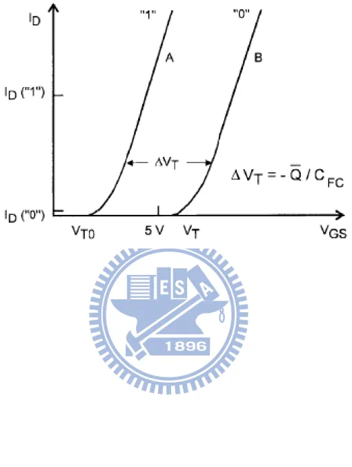
Fig 1.6 Current-Voltage characteristics of a memory device in the programmed state and erase state display the V shift and memory window.
Chapter 2
Effect of Interfacial Dipole on
SONOS-type Memory Capacitors and Nanocrystals
Memory Devices
2.1 Introduction
SONOS-type (Poly Si-Oxide-Nitride-Oxide-Silicon) flash memories have recently attracted much attention as a candidate for the next-generation. As a result of they have many advantages of operation characteristics such as, high P/E speed, low operation voltage, low power consumption, excellent retention, endurance, and disturbance [2.1-2.3]. As people demand more and more electronic technology, the pursuit of high performance and high reliability is the goal of many researchers.
In addition to, a high-k metal gate scheme for metal-oxide-semiconductor field-effect-transistors (MOSFET) above of 45nm technology is considered to replace the traditional SiO2/polysilicon based device due to the poly depletion effect [2.4] and gate
leakage for ultra thin oxide. One of serious problem of high-k/metal gate CMOS is to control the threshold voltage (VT). As we know, the VT of n and p MOSFT must be the same in
CMOS logic circuits [2.5-2.7]. Recently, the interfacial dipole with high-k/SiO2 interface has
a significant role on VFB shift due to the dipole layer formation [2.8-2.13].In they year of 2007, K. Iwamoto et al indicate that the high-k/IL-SiO2 interface plays the significant role in the VFB
control of the high-k MOS device. And Y. Kamimuta et al further use the different material as gate with different high-k material to indicate the relationship such as the Figure 2.1 (a) shows. And the band diagram of high-k/SiO2 with different high-k material is shown in
estimated to be ±-0.57±0.05, ±0.31±0.05, and 0.23±0.05eV, respectively.
There are three theories about the origin of the dipole layer at high-k/SiO2. In the years
of 2007, Sivasubramani et al considered that the dipole magnitude was determined by electronegativitiy and ionic radii of cations [2.11]. In the years of 2008, Kita and Toriumiet al reported that the areal density difference of oxygen atoms was the origin of dipole
formation at high-k/SiO2 interface [2.12]. They have predicted an effect of various oxides on VFB in
terms of interface dipole, as show in Figure 2.1(c). And in 2010, Xiolei Wang et al proposes a DCIGS (dielectric contact induced gap states) model to interpret the physical origin of dipole formation for high-k/SiO2 systems [2.13]. Although, they have different point of view on the
interfacial dipole, they did confirm that the high-k/SiO2 interface has a significant role on VFB
shift.
2.2 Experiment
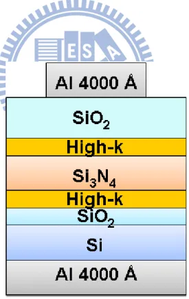
Nitride-base SONOS-type memory capacitor are fabricated on a p-type, 20 ~ 30Ω cm, (100) 150-mm silicon substrate. After RCA clean, a 35 Å tunnel oxide was thermally grown at 800 ℃ in a horizontal furnace system. Then an ultra-thin high-k film (Al2O3 5 Å, 10 Å, 20 Å,
and 30 Å or HfO2 10 Å, 30 Å) is deposited by MOCVD system or not deposited and
continuous to after that step. Next a 90 Å Si3N4 film is deposited by horizontal furnace
LPCVD system. Then an ultra-thin high-k film (Al2O3 10 Å, 20 Å, 30 Å or HfO2 10 Å, 20 Å)
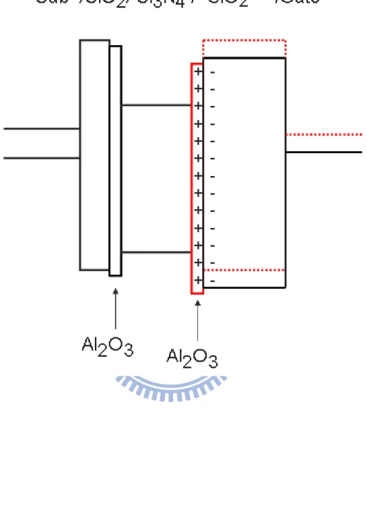
is deposited by MOCVD system or not deposited and continuous to next step. Afterward a 10nm blocking oxide is then deposited through TEOS precursor by horizontal furnace LPCVD system. Subsequently, we deposited Al as top and bottom electrode by thermal coater as well as the memory capacitor with dipole layer is finished, as the Figure 2.2 shows.
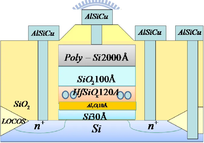
Then an example of the fabrication process of the HfO2 nano-crystal with dipole layer
20-30 Ω cm, (100) 150-mm silicon substrate. First, a 30 Å tunnel oxide was thermally grown at 800℃ in a horizontal furnace system. Then an ultrs-thin high-k layer (HfO2 or Al2O3) is
deposited by MOCVD to form dipole layer. The flow rate and pulse number of precursors is carefully modulated to obtain ~ 10 Å high-k film. Next a 120 Å amorphous HfSiOx silicate
layer was deposited by MOCVD. The samples were then subjected to RTA treatment in an N2
ambient at 950℃ for 1 min to convert the HfSiOx silicate film into the separated HfO2 and
SiO2 phase. Afterward a 100 Å blocking oxide is then deposited through TEOS precursor by
horizontal furnace LPCVD system. Subsequently, poly-Si deposition, gate patterning, n+ source/drain (S/D) implantation , p+ body implantation, activation 950℃ for 30 second, and the remaining standard CMOS procedures were completed to fabricate SONOS-type nonvolatile memory devices, as the Figure 2.3 shows.
2.3 Results and Discussion
2.3.1 Effect of Interfacial Dipole on SONOS-type Capacitor
Previously described in our nitride-base SONOS-type memory capacitor experiments, we can discuss the contents of four. First, we can discuss the influence of high-k layer between bottom oxide and trapping layer. Second, we can discuss the influence of the high-k on Si3N4. Third, we can discuss the influence of the high-k between trapping layer and top
oxide. At last, we can discuss the influence of the double dipole layer. The Cross-sectional TEM image of Si/SiO2 30 Å / Al2O3 20 Å / Si3N4 150 Å / SiO2 150Å and Si/SiO2 30 Å / Al2O3
15 Å / Si3N4 150 Å / Al2O3 20 Å /SiO2 150 Å are shown in Figures 2.4(a) and (b).
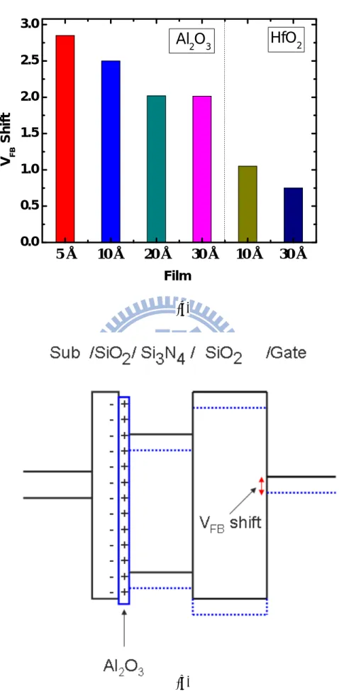
1. Discuss the influence of dipole layer between bottom oxide and trapping layer.
Figures 2.5(a) and 2.5(b) illustrate the structure of capacitors and their
Capacitance-Voltage (C-V) characteristics. The samples are deposited with Al2O3 5 Å, 10 Å,
Al2O3 or HfO2 layer causes positive VFB shift, compared with conventional SONOS capacitor.
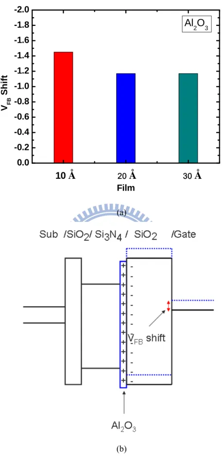
Magnitudes of dipole are ordered in monotonous decrease: Al2O3 5 Å, Al2O3 10 Å, Al2O3 20
Å, Al2O3 30 Å HfO2 10 Å, and HfO2 30 Å. The result is shown in the Figure 2.6(a). The
magnitudes of VFB shift of Al2O3 is about twice large than HfO2. Moreover, the magnitudes of
VFB shift will saturate at the dipole layer with 20 Å. Here we find that the VFB shifts is larger
when the high-k layer is thinner (>5 Å). In the beginning, we speculate that the thickness of dipole layer is more than we imagine. The equation follows as:
ox ox ms
FB
Q
C
V
/
(2-1) However, we can confirm that the thickness is not different through TEM analysis. The relationship between the VFB shifts and thickness of dipole layer may require further analysisto know why they are different with others experiments. The different of experimental procedure between ours and others are the source of dipole layer. Here, we use MOCVD and others use ALD (Atomic Layer Deposition) to deposit the dipole layer. The band diagram of this structure is shown in Figure 2.6 (b)
2. Discuss the influence of the dipole on Si3N4.
Figures 2.7(a) and 2.7(b) show the structure of capacitors and their C-V characteristics.
In Figure 2.7(b) we find the VFB of the sample of Al2O3 10 Å and HfO2 10 Å with
conventional SONOS almost the same. With the little different with of VFB, we took that as a
variation of process. After all, the gap is much smaller than previous experiments in discussion one. Therefore, we believe the dipole is substantially suppressed on Si3N4 film in
place of SiO2 in our experiments and coherence to our expectations.
3. Discuss the influence of the dipole layer between trapping layer and top oxide.
Figures 2.8(a) and 2.8(b) illustrate the structure of capacitors and their C-V
characteristics. The samples are deposited with Al2O3 10 Å, 20 Å, and 30 Å by MOCVD. We
expectations. Finally, we sort out the result showing in the Figure 2.9(a). The band diagram is shown in Figure 2.9(b). However, we still find the same situation with the previous that the VFB shift is larger when the dipole layer is thinner and also saturate at thickness 20 Å. This
result is the same as with the previous in discussion one, thus this rationale should exist some physical meaning we should go further analysis to understand why they like this.
4. Discuss the influence of the double dipole layer.
Figures 2.10(a) and 2.10(b) emerge the structure of capacitors and their C-V
characteristics. The samples are deposited with Al2O3 10 Å, 20 Å, 30 Å, and HfO2 10 Å, 30 Å
by MOCVD. Here, we contrast the sample of conventional SONOS capacitors and the sample of SONOS-type structure with Al2O3 deposition on tunneling layer, and the VFB of these
samples are between this two. The VFB shift of Al2O3 is about twice of HfO2. The band
diagram is shown in Figure 2.11. The relationship between the VFB shifts and thickness of
dipole layer are not clearly, this may be owing to our real thickness lightly thicker than expected. As a result, make this situation has already reached saturation.
2.3.2 Effect of Interfacial Dipole on Nanocrystal Memory Device
In these experiments, we find that our devices have two serious problems which are gate injection and poly-depletion. The serious gate injection problem prohibits us to analyze the device characteristics. However, in later chapters we will address these two issues.1. Poly depletion
Figure 2.12 illustrates IDS-VGS curve of the nanocrystal flash memory with Al2O3
dipole layer engineering. The on-off ratio can reach eight orders . However, we can find out the subthreshold swing (S.S.) is poor. After calculations, we get subthreshold swing equal to 611mV/dec. The ideal subthersold swing we can calculate by the equation:
dec mV C C C C q kT S S ox poly it dep / ) 1 ( 3 . 2 . . (2-2)
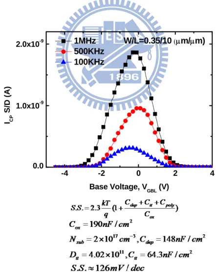
Figure 2.13 shows the charge pumping current measurement and used to calculate the value
of interface state (Dit). Therefore, we have ideal value equal to 126mv/dec .The actual value is
far worse with the ideal. We are reasonable guess that there are poly depletion issues, since use the wrong self-alignment implantation energy. However, we will change the process conditions and solve the problem in later chapters.
2. Gate injection
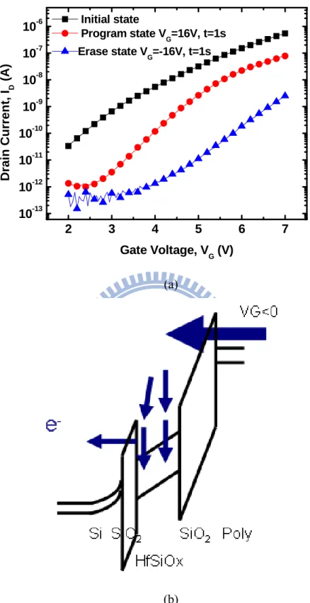
Figure 2.14(a) shows the IDS-VGS curve of the nanocrystal flash memory with
programming time 1s and erasing time 1s. We find out the erasing characteristics which are suppressed by gate injection issues. The band diagram of erasing is shown in Figure 2.14(b). We even obtain the same outcome as programming characteristics. We consider the quality of blocking oxide we adopting is worse. However, we will change the process conditions and solve the problem in later chapters.
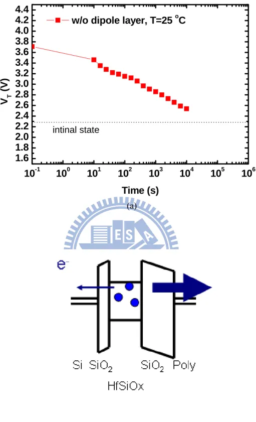
The retention characteristics of nanocrystal flash memory at room temperature (T=25℃) are illustrated in Figure 2.15(a). It results in about 80% memory window loss for 104 second retention time at room temperature. For such a bad result we are not surprised, as a result of the poor blocking oxide. We think the trapping charge is going to escape from blocking oxide, not tunneling oxide. The band diagram of retention is shown in Figure 2.15(b). In the beginning, we are thinking whether the process using is mistake. However, we confirmed that the quality of blocking is poor and use other material in later chapters.
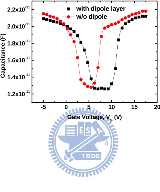
Although the serious gate injection problem prohibits us to analyze the device characteristics. By the C-V characteristics of conventional nanocrystal and the nanocrystal with dipole layer engineering flash memory is shown in Figure 2.16. Obviously, the discovery of positive VFB shift owing to Al2O3 dipole layer engineering.
2.4 Summary
In this chapter, we demonstrate the effect of interfacial dipole on SONOS flash memory capacitors on C-V characteristics. We find that the dipole of ultra thin Al2O3 and HfO2 layer
on the SiO2 tunneling layer has a positive VFB shift and on the Si3N4 trapping layer (under
SiO2 blocking layer) has a negative VFB. Furthermore, when the high-k layers are deposited on
the SiO2 tunneling layer and Si3N4 trapping layer, we can find that the value of VFB is similar
to VFB of conventional SONOS capacitors. The shift of Al2O3 is about twice of HfO2.
Moreover, the thinner high-k layer cause a larger VFB shift and saturate at 20 Å. The
relationship between the VFB shifts and thickness of dipole layer may require further analysis
to know why they are different with others experiments. When the Al2O3 dipole layer applied
in Hafnium silicate nanocrystal flash memory device, we can also find out the positive VFB
shift from C-V characteristic. Although there are gate injection and poly depletion problems in our devices, we will tackle these problems in later chapters.
References (chapter2)
[2.1] M. V. Duuren, N. Akil, M. Boutchich, and D.S. Golubovic,”New writing mechanism for reliable SONOS embedded memories with thick tunnel oxide,” in Integrated Circuit
Design and Technology and Tutorial, 2008. ICICDT 2008. IEEE International
Conference on, 2008, pp.181-184
[2.2] S. Y. Wang, H. T. Lue, P. Y. Du, C. W. Liao, E. K. Lai, S. C. Lai, L. W. Yang; T. Yang. K. C. Chen, J. Gong, K. Y. Hsieh, R. Liu, and C. Y. Lu, “Reliability and Processing Effects of Bandgap-Engineered SONOS (BE-SONOS) Flash Memory and Study of the Gate-Stack Scaling Capability,” in Device and Materials Reliability, IEEE Transactions, 2008, pp. 416-425
[2.3] T. M. Pan, and W. W. Yeh, “High-Performance High- k Y2O3 SONOS-Type Flash
Memory,” in Electron Devices, IEEE Transactions, 2008,pp. 2354-2360
[2.4] Y. Tateshita, J. Wang, K. Nagano, T. Hirano, Y. Miyanami, T. Ikuta, T. Kataoka, Y. Kikuchi, S. Yamaguchi, T. Ando, K. Tai, R. Matsumoto, S. Fujita, C. Yamane, R. Yamamoto, S. Kanda, K. Kugimiya, T. Kimura, T. Ohchi, Y. Yamamoto, Y. Nagahama, Y. Hagimoto, H. Wakabayashi, Y. Tagawa, M. Tsukamoto, H. Iwamoto, M. Saito, S. Kadomura, and N. Nagashima, “High-Performance and Low-Power CMOS Device Technologies Featuring Metal/High-k Gate Stacks with Uniaxial Strained Silicon Channels on (100) and (110) Substrates,” in Electron Devices Meeting, 2006. IEDM '06. International, 2006, pp. 1-4
[2.5] Y. C. Yeo, Q. Lu, H. Ranade Takeuchi, K.J. Yang, I. Polishchuk, T. J. King, C. Hu, S.C. Song, H.F. Luan, and D. L. Kwong, “Dual-metal gate CMOS technology with ultrathin silicon nitride gate dielectric,” in Electron Device Letters, IEEE, 2001,pp. 227-229 [2.6] I. Polishchuk, P. Ranade, T. J. King, and C. Hu;, “Dual work function metal gate CMOS
technology using metal interdiffusion,” in Electron Device Letters, IEEE, 2001, pp.444-446
[2.7] Q. Lu; R. Lin, P. Ranade, and T. J. King, Chenming Hu;” Metal gate work function adjustment for future CMOS technology,” in VLSI Technology, 2001. Digest of Technical Papers. 2001 Symposium , 2001,pp45-46
[2.8] Y. Kamimuta, K. Iwamoto, Y. Nunoshige, A. Hirano, W. Mizubayashi, Y. Watanabe, S. Migita, A. Ogawa, H. Ota, T. Nabatame, and A. Toriumi,” Comprehensive Study of VFB Shift in High-k CMOS - Dipole Formation, Fermi-level Pinning and Oxygen Vacancy Effect,” in Electron Devices Meeting, 2007. IEDM 2007. IEEE International, 2007, pp.341-344
[2.9] S. Kubicek, T. Schram, V. Paraschiv, R. Vos, M. Demand, C. Adelmann, T. Witters, L. Nyns, L. A. Ragnarsson, H. Yu, A. Veloso, R. Singanamalla, T. Kauerauf, E. Rohr, S. Brus, C. Vrancken, V. S. Chang, R. Mitsuhashi, A. Akheyar, H. J. Cho, J. C. Hooker, B.
Gendt, P. Absil, T. Hoffmann, and S. Biesemans, ” Low VT CMOS using doped Hf-based oxides, TaC-based Metals and Laser-only Anneal,” in Electron Devices
Meeting, 2007. IEDM 2007. IEEE International, 2007, pp.49-52
[2.10] K. Iwamoto, H. Ito, Y. Kamimuta, Y. Watanabe, W. Mizubayashi, S. Migita, Y. Morita, M. Takahashi, H. Ota, T. Nabatame, and A. Toriumi, ” Re-examination of Fat-Band Voltage Shift for High-k MOS Devices,” in VLSI Technology, 2007 IEEE Symposium, 2007, pp. 70-71
[2.11] P. D. Kirsch, P. Sivasubramani, J. Huang, C. D. Young, M. A. Quevedo-Lopez, H. C. Wen, H. Alshareef, K. Choi, C.S. Park, K. Freeman, M. M. Hussain, G.; Bersuker, H. R. Harris, P. Majhi, R. Choi, P. Lysaght, B. H. Lee, H. H. Tseng, R. Jammy, T. S. Boscke, D. J. Lichtenwalner, J. S. Jur, and A. I. Kingon, ” Dipole model explaining high-k/metal gate field effect transistor threshold voltage tuning,” in Applied Physics Letters, 2008, pp. 092901 - 092901-3
[2.12] K. Kita, and A. Toriumi,” Intrinsic origin of electric dipoles formed at high-k/SiO2 interface,” in Electron Devices Meeting, 2008. IEDM 2008. IEEE International, 2008, pp.1-4
[2.13] X. Wang, K. Han, W. Wang, S. Chen, X. Ma, D. Chen, J. Zhang, J. Du, Y. Xiong, and A. Huang, “Physical origin of dipole formation at high-k/SiO2 interface in metal-oxide-semiconductor device with high-k/metal gate structure,” in Applied Physics
(a) (b)
(c)
Fig. 2.1 (a) Relationship between EWF of metal gate along with n+poly-Si on high-k and SiO2. (b)Schematic band diagram of Al2O3/SiO2, HfO2/SiO2, and Y2O3/SiO2 systems [2.8]. (c)
Fig 2.2 Schematic of conventional SONOS memory capacitors with interfacial dipole layer engineering.
RCA clean
Thermal Oxide 35 Å
MOCVD ultra thin dipole layer Al
2O
3&HfO
2 LPCVD Si
3N
4150 Å
MOCVD ultra thin dipole layer Al
2O
3&HfO
2 LPCVD SiO
2150 Å
Fig 2.3 Schematic of HfO2 nanocrystal flash memory structure with interfacial dipole layer
engineering
LOCOS isolation (Active region definition, P
+Well ,Channel stop
&anti punch through& V
Tadjustment implant )
Thermal Oxide 30 Å
MOCVD Al
2O
310 Å
MOCVD HfSiO
x120 Å
RTA 950°C 60s
LPCVD SiO
2100A
Deposition Poly-Si 2000 Å
N
+Source/Drain
P
+Body Contact
Activation 950°C 30s
Passivation
Metallization
(a)
(b)
Fig 2.4 (a) Cross-sectional TEM image of Si/SiO2/Al2O3/Si3N4/SiO2. The ultra-thin Al2O3
layer is well formed upon the bottom SiO2. (b) Cross-sectional TEM image of
Si/SiO2/Al2O3/Si3N4/Al2O3/SiO2. The ultra-thin Al2O3 layer is well formed upon the bottom
(a)
(b)
Fig 2.5 (a) Schematic of capacitor structure of discussion the influence of the dipole deposit between bottom oxide and nitride trapping layer and (b) their C-V characteristics with Al2O3 5
Å, 10 Å, 20 Å, 30 Å, HfO, 10 Å, and 20 Å. -3 -2 -1 0 1 2 0.0 0.2 0.4 0.6 0.8 1.0 C ox /C ma x Gate Voltage, VG (V) SONOS Al 2O3-5 Å Al 2O3-10Å Al 2O3-20 Å Al 2O3-30Å HfO 2-10 Å HfO 2-30Å
(a)
(b)
Fig 2.6 (a) The result of VFB shift with interfacial deposit on bottom oxide in Figure 2.5(b). (b)
The band diagram of SONOS-type capacitor with interfacial deposit on bottom oxide.
0.0 0.5 1.0 1.5 2.0 2.5 3.0
HfO
2 V FB Shift FilmAl
2O
35
Å 10 Å 20 Å 30 Å 10 Å 30 Å(a)
(b)
Fig 2.7 (a) Schematic of capacitor structure of discussion the influence of the dipole deposit on nitride trapping layer and (b) their C-V characteristics with AlO 10 Å and HfO 10 Å.
-3.5 -3.0 -2.5 -2.0 -1.5 -1.0 -0.5 0.0 0.0 0.2 0.4 0.6 0.8 1.0 C ox /C max Gate Voltage, VG (V) SONOS HfO2-10Å Al2O3-10Å
(a)
(b)
Fig 2.8 (a) Schematic of capacitor structure of discussion the influence of the dipole deposition between nitride layer and top oxide and (b) their C-V characteristics with Al2O3 10
Å, 20 Å, and 30 Å. -5 -4 -3 -2 -1 0 0.0 0.2 0.4 0.6 0.8 1.0 C ox /C max Gate Voltage, V G (V) SONOS Al2O3-10 Å Al2O3-20 Å Al2O3-30 Å
(a)
(b)
Fig 2.9 (a) The result of VFB shift with interfacial deposit on nitride layer in Figure 2.8(b). (b)
The band diagram of SONOS-type capacitor with interfacial deposit on nitride layer.
0.0 -0.2 -0.4 -0.6 -0.8 -1.0 -1.2 -1.4 -1.6 -1.8 -2.0 V FB Shift Film
Al
2O
3 10Å
2 0Å
3 0Å
(a)
(b)
Fig 2.10 (a) Schematic of capacitor structure of discussion the influence of the double dipole layer deposition on bottom oxide and nitride layer and (b) their C-V characteristics with Al2O3
10 Å, 20 Å,30 Å, HfO2,10 Å , and 30 Å on nitride layer.
-3 -2 -1 0 1 0.0 0.2 0.4 0.6 0.8 1.0 C ox /C ma x Gate Voltage, V G (V) SONOS Al2O3-10Å Al2O3-20 Å Al2O3-30 Å HfO2-10 Å HfO2-30 Å Only Bottom Al2O3-10 Å
Fig 2.11 The band diagram of SONOS-type capacitor with interfacial deposit on bottom oxide and on nitride layer.
Fig 2.12 IDS-VGS curve of the nanocrystal flash memory with Al2O3 dipole layer engineering.
Fig 2.13 Plots of ICP vs VGBLl for the HfO2 nanocrystal memory cell with different frequency
and the parameter after calculate.
0 2 4 6 8 10 12 10-13 10-12 10-11 10-10 10-9 10-8 10-7 10-6 10-5 10-4 10-3
with dipole layer W/L=10/0.6m S.S.=611 mV/dec Drain Current, I D (A ) Gate Voltage, VG (V) V D=0.05 V VD=0.533 V VD=1.02 V VD=1.5 V -4 -2 0 2 4 0.0 1.0x10⁻⁹ 2.0x10⁻⁹ I CP S/D (A) Base Voltage, VGBL (V) 1MHz 500KHz 100KHz W/L=0.35/10 m/m)
(a)
(b)
Fig 2.14 (a) IDS-VGS curve of the nanocrystal flash memory with programming time 1s and
erasing time 1s. (b)The band diagram of nanocrystal memory at erasing operation and have seriously gate injection.
2 3 4 5 6 7 10-13 10-12 10-11 10-10 10-9 10-8 10-7 10-6 Dr ain Curr ent , I D (A ) Gate Voltage, V G (V) Initial state Program state VG=16V, t=1s Erase state VG=-16V, t=1s
(a)
(b)
Fig 2.15 (a) Retention characteristics of nanocrystal flash memory at room temperature (T=25℃) with 104 second. (b) The band diagram of retention. The losing charge is mainly escape by blocking oxide not tunneling oxide.
10-1 100 101 102 103 104 105 106 1.6 1.8 2.0 2.2 2.4 2.6 2.8 3.0 3.2 3.4 3.6 3.8 4.0 4.2 4.4 V T (V) Time (s)
w/o dipole layer, T=25 oC
Fig 2.16 C-V characteristics of our nanocrystal and nanocrysta with dipole layer engineering flash memory. -5 0 5 10 15 20 1.2x10⁻¹¹ 1.4x10⁻¹¹ 1.6x10⁻¹¹ 1.8x10⁻¹¹ 2.0x10⁻¹¹ 2.2x10⁻¹¹ Capacitance (F) Gate Voltage, VG (V)
with dipole layer
w/o dipole
Chapter 3
Characteristic of HfO
2Nanocrystals Nonvolatile
Flash Memory with High-k Blocking Layer
3.1 Introduction
Flash memory has been the subject of aggressive scaling during the past decade. The SONOS-type (Poly Si-Oxide-Nitride-Oxide-Silicon) structure memories, which include nitride and nanocrystal memories, have attracted much attention for their application [3.1-3.4] due to many advantages. In order to meet the performance requirements of future generation, one of the nearest major changes will concern the engineering of Interpoly Dielectric (IPD or we can say blocking layer) stack. The optimization of the blocking layer is necessary to avoid electron tunneling through the blocking oxide during the erase condition, which in turn causes an erased problem [3.5-3.6].
Since the high-k dielectric exhibits a significantly lower leakage current density for the relatively thinner effective oxide thickness, we can increase both the thickness and the electric field for the electric field for the tunnel oxide at the same operating voltage. Therefore, SONOS-type flash device with high-k blocking layer provides a faster P/E speed and longer data retention time [3.7-3.8]. But as we know, the higher permittivity the smaller energy band gap in general. For a example, HfO2 has high permittivity (~25) and can increase the electric
field for tunneling oxide, however, it is not appropriate blocking layer due to the small energy band gap (~5.2eV). On the contrary, Al2O3 offers the sufficient energy gap (~8) to block the
hole and electron current with low permittivity (~9). The band diagrams are shown in Figures
(a), and (b) .Therefore, how to choose the advantages of both is very important. In addition to,
cause to crystallize, and further result leakage current and trapping charge.
3.2 Experiment
A capacitor with blocking layer material as gate oxide are fabricated on a p-type, 20 ~ 30Ω cm, (100) 150-mm silicon substrate. After RCA clean, the 15nm Al2O3 and HfAlOx with
pulse ratio Al: Hf= 3: 1 were deposited by MOCVD. The post deposition anneal with 950°C 30s embedded N2. At last, we deposited Al as top and bottom electrode by thermal coater. The
structure is shown inFigure 3.2
An example of the fabrication process of the HfO2 nano-crystal nonvolatile memory
devices is demonstrated by a LOCOS isolation process on a p-type, 20-30 Ω cm, (100) 150-mm silicon substrate. First, a 30 Å tunnel oxide was thermally grown at 800℃ in a horizontal furnace system. Next a 120 Å amorphous HfSiOx silicate layer was deposited by
MOCVD. The samples were then subjected to RTA treatment in an N2 ambient at 950° C for 1
min to convert the HfSiOx silicate film into the separated HfO2 and SiO2 phase. Their
compositions were identified using X-ray photoelectron (XPS). A 100 Å Al2O3 and HfAlOx
was then deposited through MOCVD. Subsequently, poly-Si deposition, gate patterning, n+ source/drain (S/D) implantation, p+ body implantation, activation 950℃ 30 second, and the remaining standard CMOS procedures were completed to fabricate the HfO2 nano-crystal
nonvolatile memory device. The nanocrystal flash memory structure is shown in Figure 3.3
3.3 Results and Discussion
3.3.1 Material Analysis of Al
2O
3and HfAlO
xBlocking Layer
First we use the MOS capacitor structure to analyze the material of blocking layer, such the Figure 3.2 shows. Because our device have to endure the high temperature S/D annealing