金氧半場效電晶體 (MOSFET) 閘極及源/汲極製程改善之研究
132
0
0
全文
(2) 金氧半場效電晶體 (MOSFET) 閘極及源/汲極製程改善之 研究. 研究生: 張俊傑. 指導教授: 謝宗雍 教授 國立交通大學 材料科學與工程學系. 摘要 當半導體元件尺寸縮小至 90 奈米以下時,對材料和製程控制的 品質要求愈來愈嚴格。金氧半場效電晶體 (MOSFET) 是超大型積體 電路例如微處理器及記憶體中最重的元件,而閘極及源/汲極是其最 主要的組成。因此,閘極及源/汲極材料的品質將直接影響到元件的 性能。在本論文中,我們針對閘極及源/汲極材料製程進行改善,以 改善元件性能。 針對多晶矽 (Polysilicon) 閘極,我們提出堆疊式多晶矽薄膜沉 積方法,此方法是在多晶矽薄膜上沉積非晶矽 (Amorphous silicon) 薄膜。實驗證實,此方法可有效降低多晶矽薄膜表面粗糙度,並且可 改善非晶矽薄膜在加熱後引起的表面突起及傳統多晶矽薄膜造成的 高角度晶界 (High angle grain boundary)問題。電性測試結果亦顯示此 方法明顯比傳統多晶矽薄膜具有更低的漏電流問題。 對源/汲極,我們提出兩階段加熱的氧化介層矽化法. 2.
(3) (Oxide-mediated silicidation),發現此方法可形成緻密及具有平坦表面 的二矽化鈷 (CoSi2) 薄膜,並且呈現均勻性奈米晶粒尺寸分佈。此製 程若使用氮化鈦保護層 (TiN capping),可形成平均 5 奈米的晶粒尺 寸;若使用鈦保護層 (Ti capping) 可形成平均 4 奈米的晶核尺寸。我 們並針對其形成機制作探討發現,氧化介層 (SiOx) 形成一個單向的 阻絕層,只允許鈷擴散進入矽基材,但阻擋矽向外擴散。鈷和二矽化 鈷同時存在於氧化介層與矽基材間,表示鈷的擴散速率高於矽化鈷的 反應速率。鈦會吸收氧化介層的氧原子弱化氧化介層而加強鈷的擴散 速率,因此鈦與氧化介層的反應速率須妥善控制以形成具有足夠厚度 及低阻值的二矽化鈷薄膜。若反應速率過快,易形成高阻值的矽化鈷 (CoSi);若反應速率過慢,則無法形成足夠厚度的二矽化鈷薄膜。 最後在鈷薄膜的沉積過程中,發現了形狀對稱的奈米錐狀物結 構,此錐狀物共具有兩種不同的型式。這種錐狀物只發生在鈷的六方 最密堆積 (hcp) 結構上,並且是長在具有平行柱狀結構的鈷薄膜上。 其成核機制是被應變能,濺鍍原子及離子的動能所影響;成長機制則 主要是由最小表面能影響。. 3.
(4) The Process Improvement of Gate and Source/Drain Electrodes of a MOSFET Device Student: Juin-Jie Chang. Advisor: Dr. Tsung-Eong Hsieh. Department of Materials Science and Engineering, National Chiao-Tung University. Abstract As the semiconductor device was scaled down to below 90 nm, the demand of material quality and process control becomes more and more strict. The metal-oxide-semiconductor field-effect transister (MOSFET) is the most important device for ultra-large-scale integrated circuits (ULSI) such as microprocessors and semiconductor memories. The gate and source/drain electrodes are the main parts of a MOSFET, their material quality will directly influence the device performance. Hence, in this thesis, we focus on the process improvement of Gate and Source/drain electrodes of a MOSFET device. For the polysilicon gate, we proposed a new stacked polysilicon film process combines polysilicon with amorphous silicon films and found doped stacked poly-Si films with lower surface roughness and smoother poly-Si/polyoxide interface than doped a-Si and conventional poly-Si films. This new stacked poly-Si film has the poor recrystallization- induced crystallinity as in a-Si but no protrusion on surface and no apparent high angle grain boundaries. Results of electrical breakdown voltage. 4.
(5) measurements also show that the doped poly-Si film stack has a better performance than the doped conventional poly-Si film. For the source/drain, a oxide-mediated silicidation method with two-step annealing was developed to forms a dense and smooth with homogeneous nano-grain size distribution CoSi2 thin film. The nanocrystalline CoSi2 thin film with average grain size of 5 nm with homogeneous nano-grain size distribution can be directly formed by this method with a TiN capping layer; The average nucleus-size of about 4 nm with uniform island size distribution also can be formed by this method with a Ti-capping layer. The underline mechanism of diffusion and nucleation also be studied. Electroscopic imaging in transmission electron microscopy shows that SiOx act as a one-way diffusion barrier in oxide-mediated silicidation which only allows Co diffuse into Si substrate but inhibits Si diffuse out. X-ray photoelectron spectroscopy analysis shows that unreacted Co coexists with CoSi2 at the interface between the SiOx layer and Si substrate. Ti capping layer can absorbs oxygen from the SiOx layer, which induces weak points in the SiOx layer and then enhances Co diffusion as well as CoSi2 formation. The control of the reactions between Ti and SiOx is significant because low reaction rate cannot form enough thickness of CoSi2 film whereas high reaction rate tends to form highly resistive CoSi phase. Finally, a very interest pyramid-like nanostructure was found during cobalt thin. 5.
(6) film deposition by a dc magnetron sputtering. The pyramid-like nanostructures were found to form on top of columnar grains only when cobalt is hcp phase. There are two types of faceted nanostructures on Si(001) substrates, where type I is composed of 1 013, 2 201 and 02 21 and type II is composed of 1 013, 01 1 1and 1 1 01 planes,. with the basal plane of 10 1 0. Their nucleation is enhanced by a complex function of strain, adatom energy and ion sputtering and growth is significantly determined by the minimum surface configuration of the structure.. 6.
(7) 誌. 謝. 特別感謝指導教授謝宗雍教授歷年來在學業的指導及生活上的 關心,成大材料所劉全璞教授和 TSMC 王英郎博士在實驗及論文上的 指導協助,暨南大學吳幼麟教授在電性測試及研討會論文寫作上的指 導,TSMC 長官游友仁先生的支持,讓我得以繼續學業。另外感謝成大 材料所陳世偉同學在部分實驗上的共同合作,激發出了許多新的觀念 及想法,尤其在氧化介層矽化法及錐狀物的研究上,陸續發表了幾篇 論文。還有感謝 TSMC 蔡俊琳,許永隆,李馥夙,張惠華,劉偉仁,曾德 富,陳燕銘,林士琦,蕭文助,張簡旭珂,王志欽先生及所有學弟妹的幫 忙。 感謝父母多年來的養育之恩, 及家人的鼓勵與支持。最後特別 感謝學長簡安的關心及在背後默默付出的妻子及可愛的小女兒,陪我 一起走過了人生中最低潮的時期。。. 7.
(8) Contents Abstract (in Chinese). 2. Abstract (in English). 4. Acknowledge (in Chinese). 5. Contents. 8. Table lists. 11. Figure Captions. 11. Chapter 1. Chapter 2. Introduction 1-1 Motivation. 18. 1-2. 22. Thesis Outline. Modified Polycrystalline Silicon Chemical-vapor Deposition Process for Improving Roughness at Oxide/Polycrystalline Silicon Interface. Chapter 3. 2-1 Introduction. 25. 2-2 Experimental Details. 27. 2-3. 28. Results. 2-4 Discussion. 30. 2-5 Conclusions. 32. Direct CoSi2 Thin Film Formation with Uniform 8.
(9) Nanograin-sized Distribution by Oxide-mediated Silicidation. Chapter 4. 3-1 Introduction. 34. 3-2 Experimental Details. 36. 3-3 Results and Discussion. 37. 3-4 Conclusions. 41. The Study of Diffusion and Nucleation for CoSi2 Formation by Oxide-mediated Cobalt Silicidation. Chapter 5. 4-1 Introduction. 42. 4-2 Experimental Details. 43. 4-3 Results and Discussion. 44. 4-4 Conclusions. 45. Uniform CoSi2 Nano-nucleus Formation by Oxide-mediated Silicidation with a Ti Capping Layer. Chapter 6. 5-1 Introduction. 51. 5-2 Experimental Details. 52. 5-3 Results and Discussion. 53. 5-4 Conclusions. 56. The Study of Diffusion and Quality Control for CoSi2 Formation by Oxide-mediated Cobalt Silicidation with Ti 9.
(10) Capping. Chapter 7. 6-1 Introduction. 57. 6-2 Experimental Details. 58. 6-3 Results and Discussion. 59. 6-4 Conclusions. 63. Formation of Pyramid-like Nanostructures during Cobalt Film Growth by Magnetron Sputtering. Chapter 8. 7-1 Introduction. 65. 7-2 Experimental Details. 66. 7-3 Results and Discussion. 66. 7-4 Conclusions. 72. Conclusions and Suggestions for Future Research 8-1 Conclusions. 73. 8-2. 75. Suggestions for Future Research. References. 76. Tables. 90. Figures. 91. Vita. 127. Publication Lists. 128. 10.
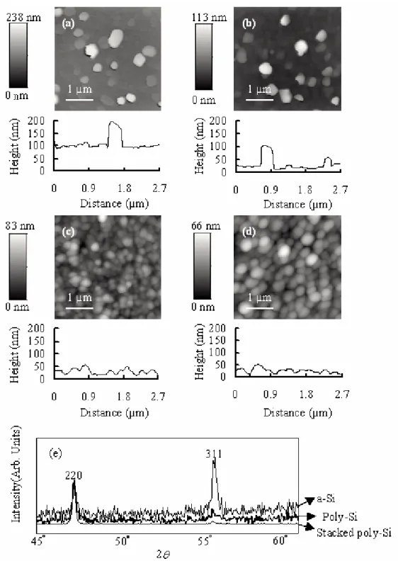
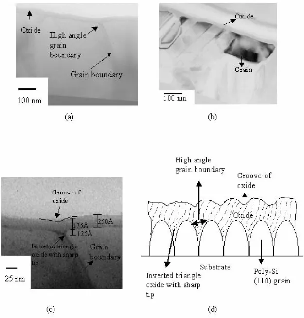
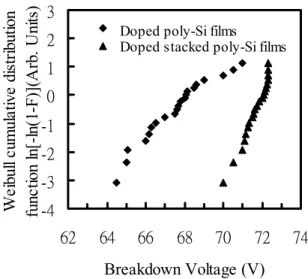
(11) Table Lists Table 6-1: Free enthalpies of oxide formation at 1030 K in kJ/mol O2.. Figure Captions Chapter 1 Fig. 1-1:. A simple schematic representation of a MOSFET device.. Chapter 2 Fig. 2-1: AFM contact mode images and corresponding line scans of doped a-Si films deposited at (a) 540 and (b) 560 °C; of (c) doped poly-Si films deposited at 630 °C and (d) stacked poly/poly-Si/a-Si films. X-ray diffraction results for the stacked poly/poly-Si/a-Si films are presented in (e). Fig. 2-2: TEM cross-section micrographs of (a) doped poly-Si and (b) doped stacked poly-Si (c) the magnified image of (a) around the grain boundary region. A schematic representation of the interface is detailed in (d). Fig. 2-3: Weibull plots of electrical characteristics of doped stacked poly-Si film versus conventional poly-Si film.. 11.
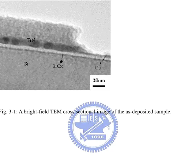
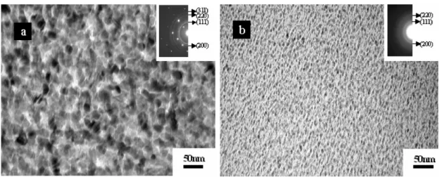
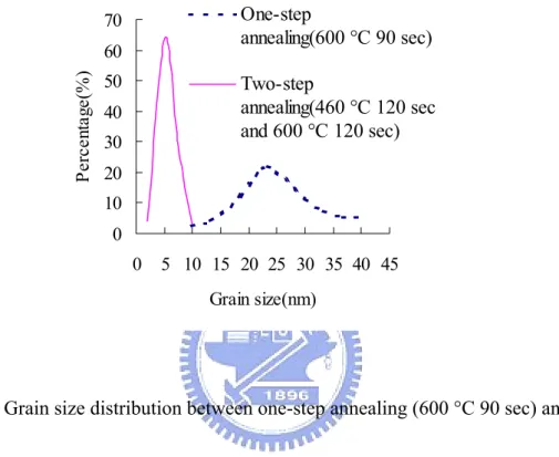
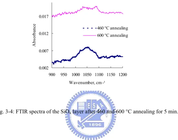
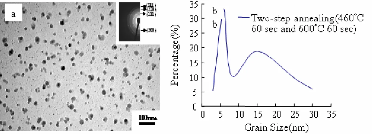
(12) Chapter 3 Fig. 3-1: A bright-field TEM cross sectional image of the as-deposited sample. Fig. 3-2: TEM Bright-field plan-view images and diffraction patterns of the samples upon annealing with the TiN capped layer, unreacted cobalt and SiOx removed, where the annealing conditions are (a) 600 °C 90 sec (b) firstly 460 °C 120 sec and then 600 °C 120 sec. Fig. 3-3: Grain size distribution between one-step annealing (600 °C 90 sec) and two-step annealing (firstly 460 °C 120 sec and then 600 °C 120 sec). Fig. 3-4: FTIR spectra of the SiOx layer after 460 and 600 °C annealing for 5 min. Fig. 3-5: (a) TEM Bright-field plain-view images with diffraction pattern and (b) the grain size distribution of the sample upon annealing with TiN capped layer, unreacted cobalt and SiOx removed where the annealing conditions are firstly 460 °C 60 sec and then 600 °C 60 sec.. 12.
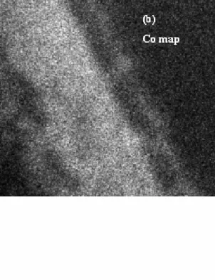
(13) Chapter 4 Fig. 4-1: (a) A cross-sectional TEM image of the sample without Si implantation annealed at 600 °C for 90 sec, with ESI elemental maps for (b) Co and (c) Si. Fig. 4-2: A bright-field plan-view TEM image and diffraction pattern of the reactive silicide of the sample without Si implantation upon annealing at 600 °C for 90 sec. Fig. 4-3: A cross-sectional TEM image of the sample without Si implantation for the annealing condition of 600 °C for 90 sec. Fig. 4-4: A bright-field cross-sectional TEM image of the sample without Si implantation for the annealing condition of 600 °C for 60 sec. Fig. 4-5: A bright-field plan-view TEM image of the reactive silicide of the sample without Si implantation upon annealing at 600 °C for 60 sec. Fig. 4-6: A bright-field cross-sectional TEM image of the sample without Si implantation for the annealing condition of 460 °C for 120 sec. Fig. 4-7: (a) XPS results from two samples with and without Si implantation in the Si substrate with unreacted TiN, Co and SiOx removed, where the annealing condition was 460 °C for 60 sec followed by 600 °C for 60 sec annealing. The deconvolution of the main peak in (a) is shown in (b) for the sample with Si implantation and (c) for the sample without Si implantation.. 13.
(14) Chapter 5 Fig. 5-1: (a) A TEM bright-field plan-view image with the corresponding diffraction pattern and (b) nucleus size distribution of the sample upon annealing at 600 °C for 120 sec with the TiN capped layer, unreacted cobalt,Ti and SiOx removed. Fig. 5-2: (a) and (b) TEM bright-field cross-sectional images from two different areas of the sample upon 600 °C 120 sec annealing. Fig. 5-3: TEM bright-field plain-view images of the samples upon annealing with the TiN capped layer, unreacted cobalt,Ti and SiOx removed, where the annealing condition are (a) 600 °C 240 sec (b) firstly 460 °C 240 sec and then 600 °C 240 sec; (c) nucleus size distribution for one-step annealing (600 °C 240 sec) and two-step annealing (firstly 460 °C 240 sec and then 600 °C 240 sec) Fig. 5-4: FTIR spectra of the as-deposited SiOx layer and that upon 460 °C annealing for 4 min. Fig. 5-5: (a) A TEM bright-field plan-view image and (b) Nucleus size distribution of the sample upon annealing at 460 °C for 120 sec followed by 600 °C 240 sec with TiN capped layer, unreacted cobalt and SiOx removed.. 14.
(15) Chapter 6 Fig. 6-1: A bright-field TEM cross sectional image of the as-deposited Ti/Co/SiOx sample. Fig. 6-2: (a) A bright-field TEM cross sectional image of the Ti/Co/SiOx sample after annealing at 460 °C for 120 sec. (b) The magnified high resolution TEM image of (a). Fig. 6-3: A bright-field TEM cross sectional image of the Ti/Co/SiOx sample after annealing at 460 °C for 300 sec. Fig. 6-4: (a) A bright-field TEM cross sectional image of the TiN/Co/Ti/Co/SiOx/Si multilayered sample after 600 °C 240 sec annealing. (b) A bright-field TEM plain-view image and diffraction pattern of the reactive silicide of the sample in (a) with all the other layers removed. (c) AES depth profiles of the sample in (a). Fig. 6-5: A bright-field TEM cross sectional image of the Ti/Co/SiOx sample after annealing at 460 °C for 300 sec followed by 600 °C 300 sec.. 15.
(16) Chapter 7 Fig. 7-1: SEM plan-view images of Co thin films as a function of substrate bias for (a) –30 V (b) – 40 V (c) – 50 V (d) – 60 V. Fig. 7-2: SEM plan-view images of Co thin films as a function of applied power for (a) 40 W (b) 50 W (c) 60 W (d) 70 W. Fig. 7-3: SEM cross-sectional images of Co thin films as a function of applied power for (a) 40 W (b) 50 W (c) 60 W (d) 70 W. Fig. 7-4: TEM cross-sectional image and diffraction pattern of the pyramid-like nanostructures. Fig. 7-5: TEM bright-field image and diffraction patterns of Co thin films deposited at (a) dts = 6 cm, for ε-Co (hcp), (b) dts = 10 cm, for α-Co (fcc). Fig. 7-6: SEM plan-view images showing faceted planes of the pyramid-like nanostructures on Co thin films for (a) type I and (b) type II; (c) Schematic diagram of two types of nanostructures with detailed indices assigned for the faceted planes and edge directions. Fig. 7-7: XRD diffraction intensity ratio for four main different planes as a function of substrate bias for a fixed applied power of 50 W. Fig. 7-8: SEM plan-view images of Co thin films as a function of thickness for (a) 1260 nm (b) 1080 nm (c) 900 nm (d) 720 nm. Fig. 7-9: SEM plan-view images of Co thin films deposited as a function of applied 16.
(17) power for (a) 60 W (b) 70 W (c) 80 W (d) 90 W at the deposition distance of 10 cm. Fig. 7-10: SEM plan-view images of Co thin films deposited on Si (111) substrates, as a function of applied power for (a) 75 W (b) 125 W.. 17.
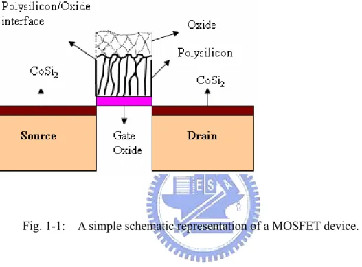
(18) Chapter 1 Introduction 1.1 Motivation The metal-oxide-semiconductor field-effect transister (MOSFET) (Fig.1-1) is the most important device for ultra-large-scale integrated circuits (ULSI) such as microprocessors and semiconductor memories. The main performance criteria of a digital MOS ICs are speed, power dissipation and device packing density. In order to get highest performance at lowest cost, reduction in device size has been the chief vehicle. But when the device size was shrunken, it suffer from more severe electrical issues, such as leakage current, higher contact resistance, circuit speed degradation …etc.[1]. To reduction these issues, the demand of material quality and process control becomes more and more strict. The gate and source/drain are the main parts of a MOSFET, their material quality will directly influence the device performance. Hence, how to improve the material quality of Gate and Source/Drain is very important. For the gate electrodes of a MOSFET, polysilicon (poly-Si) films formed by low pressure chemical-vapor deposition with silane (SiH4) was widely used in a metal-oxide-semiconductor (MOS) gates. The electrical performance of poly-Si is. 18.
(19) determined strongly by its microstructure, which depends on deposition parameters [2-5]. It was well known that the surface roughness of poly-Si degrades the electrical characteristics of dielectric film on poly-Si [6-8]. Results of many previous studies showed that amorphous silicon(a-Si) has lower surface roughness than poly-Si [9-13]. However, after annealing or doping (e.g., with phosphorus or boron), the recrystallized a-Si film will exhibit some protrusions on the surface, which is induced by (311) texture and results in a non-uniform surface. Although such problem does not occur in doped poly-Si film deposited at temperatures > 600 °C because of their better crystallinity and the (110) columnar structure [12,14], they tend to contain high-angle grain boundaries at the oxide/poly-Si interface. This will lead to non-uniform oxide film surface after oxidation and induce local electric field enhancement. Hence, we try to develope a stacked poly-Si film process to improve both the (311) texture issue of doped a-Si and the high-angle grain boundary issue of doped poly-Si film. For the source/drain, in order to reduce the contact resistant, cobalt silicide was widely applied in ULSI technology because its characteristic of low bulk electrical resistivity, good lattice match with Si. However normal polycrystalline cobalt silicide process still suffers from some serious issues such as agglomeration, silicon consumption, leakage current. Especially, the agglomeration issue will become more. 19.
(20) critical for ULSI technology below 90 nm because of the limitation of line width and shallow source/drain junction. The agglomeration will induce large-grain CoSi2 formation and hence resistance degradation. [15,16] Epitaxy CoSi2 has been expected to resolve this problem due to its excellent thermal stability. Recently, Tung [17-19] has proposed oxide mediated epitaxy (OME) technique, which can be used to form good quality of epitaxial CoSi2 and is compatible with conventional ULSI processing.. The OME method involves with. firstly the deposition of a Co thin layer (1-3 nm) onto a Si surface covered with a thin SiOx layer grown in an aqueous peroxide solution followed by annealing at 500-700 °C. However, the thickness of the epitaxial CoSi2 layers produced by a single OME process was limited to ~11nm. Thicker epitaxial CoSi2 films demand repeating deposition and annealing processes using the thin CoSi2 layer formed from the first deposition as a template. In addition, the cobalt deposition and annealing processes need to be performed under ultra-high vacuum environment [17-19], which then causes high cost in production. In addition to epitaxial CoSi2, alternatively, polycrystalline CoSi2 via the same OME process in a lower vacuum environment has also been shown to provide advantages. For example, low resistive CoSi2 is formed directly at a lower annealing temperature of 500-700 °C bypassing high resistive phases of CoSi and Co2Si [15,16].. 20.
(21) Compared to the conventional higher temperature annealing method; the CoSi2 layers is dense with smooth surface [17-19]. Therefore, to produce a polycrystalline CoSi2 phase via the OME process is more cost-effective. Xiao et al. [20] and Sun et al. [21] reported that smaller grain size and more uniform grain size distribution exhibit lower grain boundary energy and larger interfacial energy favorable for the thermal stability of silicide. In other words, CoSi2 agglomeration or recrystallization along its grain boundary can be reduced [22]. Therefore, developing polycrystalline CoSi2 with smaller grain size and better size uniformity is still a main stream for the further improvement in the current IC technology. Especially for the ULSI technology below 90 nm, nanograin-size CoSi2 is requested to prevent large-grain CoSi2 induced resistance degradation [21-23]. Hence, we try to modify OME method which was called “oxide-mediated silicidation” to produce nanograin-size CoSi2 with more homogeneous size distribution. In addition, Kim et al. [24,25] found that using Ti-capping can form a thicker epitaxial CoSi2 layer (40~50 nm) directly without repeating Co deposition and annealing processes. It is because Ti can absorb oxygen in Co layer and weaken the SiOx layer to enhance Co diffusion into Si substrate [26,27]. Hence, we also try to use a Ti-capping layer in the oxide-mediated silicidation process and compare to the TiN-capping layer.. 21.
(22) Finally, a very interest pyramid-like nanostructure was found during the Co deposition process. The cobalt nanostructures might be applied in magnetic recording media or carbon nanotube (CNT) growth as the most active catalytic site [28]. In addition, metal with a sharp tip can also be applied in the field-emission flat panel displays [29-31], so a study was focused on this structure.. 1.2 Thesis Outline In this thesis, we try to improve roughness of the poly-gate of a MOSFET by improving the polysilicon deposition process, and source/drain contact resistance by a oxide-mediated silicidation method to form homogeneous nanograin-size cobalt disillicide thin film. Finally, to study the formation mechanism of a pyramid-like nanostructure during Co deposition. In chapter 2, a new modified low pressure chemical-vapor deposition process for stacked polysilicon films is developed. The proposed stacked film process combines polysilicon with amorphous silicon films. In this process, polysilicon film was deposited first at 630 °C, followed by a continuous temperature decrease down to 560 °C for the deposition of amorphous silicon film. It was found that the doped stacked polysilicon films deposited by this process result in lowering of surface roughness.. 22.
(23) In chapter 3, a multilayer (Co/SiOx/Si) sample with TiN capping layer was studied by different annealing conditions. The nanocrystalline CoSi2 thin film with average grain size of 5 nm can be directly formed from this multilayer with the SiOx as a mediated layer by annealing at 460 °C for 120 sec followed by 600°C 120 sec. Chapter 4 try to explain the nucleation and diffusion mechanism of oxidemediated silicidation. In chapter 5, a multilayer (TiN/Co/Ti/Co/SiOx/Si) sample with Ti interlayer was studied by different annealing conditions. The nucleation stage toward CoSi2 with average island size of about 4 nm and uniform island size distribution is obtained from this multilayer with the SiOx as a mediated layer by annealing at 460 °C for 240 sec followed by 600°C 240 sec. Chapter 6 discusses the mechanism for the enhancement of CoSi2 thin film formation and film quality control by oxide-mediated silicidation with a Ti-capping layer. It is found that Ti absorbs oxygen from the SiOx layer, which induces weak points in the SiOx layer and then enhances Co diffusion as well as CoSi2 formation. The control of the reactions between Ti and SiOx is significant because low reaction rate cannot form enough thickness of CoSi2 film whereas high reaction rate tends to form high resistive CoSi phase. 23.
(24) In chapter 7, the formation mechanism of a pyramid-like nanostructure was discussed. It was found that during Cobalt thin film deposition by dc magnetron sputtering, pyramid-like nanostructures were found to form on top of columnar grains only when cobalt is hcp phase. There are two types of faceted nanostructures on Si(001) substrates, where type I is composed of 1 013, 2 201 and 02 21 and type II is. composed of 1 013, 01 1 1and 1 1 01 planes, with the basal plane of 10 1 0. Finally, conclusion and suggestion for future research are given in chapter 8.. 24.
(25) Chapter 2. Modified Polycrystalline Silicon Chemical-vapor Deposition Process for Improving Roughness at Oxide/Polycrystalline Silicon Interface. 2.1 Introduction Polysilicon (poly-Si) films formed by low pressure chemical-vapor deposition with silane (SiH4) was widely used in integrated circuits for various applications, such as metal-oxide-semiconductor (MOS) gates, interconnects, resistors, emitter contacts,...etc. Other applications include photovoltaic conversion thin film transistor for large area liquid-crystal displays. The electrical performance of poly-Si is determined strongly by its microstructure, which depends on deposition parameters [1-4]. It was well known that the surface roughness of poly-Si degrades the electrical characteristics of dielectric film on poly-Si [5-7]. For devices adopting the double poly-Si floating-gate structure, the polyoxide requires a low leakage current and high breakdown electric field to obtain adequate data retention characteristics [6,8-9]. However, a non-uniform polyoxide film thickness and rough surface morphology at the oxide/poly-Si interface can cause the. 25.
(26) polyoxide to have a higher leakage current and lower dielectric breakdown field than those of silicon dioxide grown from a single crystalline silicon substrate [10-12]. This phenomenon is attributed to local electric field enhancement at the rough oxide/poly-Si interface. Moreover, the surface roughness of oxide/poly-Si interface would be enhanced after thermal oxidation [12-14]. Therefore, how to reduce the roughness of oxide/poly-Si interface is a critical issue to device performance. Results of many previous studies showed that amorphous silicon(a-Si) has lower surface roughness than poly-Si [15-19]. However, after annealing or doping (e.g., with phosphorus or boron), the recrystallized a-Si film will exhibit some protrusions on the surface, which is induced by (311) texture and results in a non-uniform surface. Although such problem does not occur in doped poly-Si film deposited at temperatures > 600 °C because of their better crystallinity and the (110) columnar structure [18,20], they tend to contain high-angle grain boundaries at the oxide/poly-Si interface. This will lead to non-uniform oxide film surface after oxidation and induce local electric field enhancement. In this investigation, we developed a stacked poly-Si film process to improve both the (311) texture issue of doped a-Si and the high-angle grain boundary issue of doped poly-Si film. Surface roughness and oxide/poly-Si interface are analyzed by atomic force microscope (AFM) and transmission electron microscope (TEM). The. 26.
(27) electrical performance of thermally-grown oxide on these two different doped poly-Si films was tested by an Al-gate nitride/oxide/poly-Si MOS capacitor structure. The mechanisms leading to the improvements in roughness and electrical performance will be discussed.. 2.2 Experimental Details All the samples used in this experiment were prepared by low pressure chemical-vapor deposition process and the deposition process was carried out in an induction-heated hot-wall horizontal reactor using mono-silane (SiH4) gas as a silicon source. P-type (100)-oriented silicon wafers with a resistivity of 8~12 ohm-cm were used as substrates. The conventional poly-Si films were deposited at a fixed temperature (630 °C) while a-Si films were deposited at two different temperatures: 540 °C and 560 °C and all the deposition pressure was 0.11 torr. The thickness of the poly-Si and a-Si films were about 4000 Å and 3000 Å, respectively, irrespective of the deposition temperature. According to the results on the phase dependence of deposition condition [15,17], we have chosen the deposition temperature of 560 °C and an even lower temperature of 540 °C to ensure that the as-deposited phase is a-Si. The stacked poly-Si films were deposited at 630 °C for 30 min., before decreasing the temperature down to 560 °C with a rate of 3 °C / min. The temperature was then held at 560 °C for 60 min without interrupting the deposition process, the total thickness. 27.
(28) was about 4000 Å. The as-deposited film was then doped with n-type phosphorus using POCl3 gas at 950 °C and atmospheric pressure in an induction-heated hot-wall horizontal reactor. After a 5 % HF solution deglazing for 3 min and RCA SC-1/SC-2 cleaning [21], atomic force microscope (Topometrix Explorer) with a resolution of 300 x 300 pixels was employed in contact mode to analyze the surface roughness. TEM (Phillips Tecnai 20 with field emission gun) interface analysis was made after oxidizing the doped poly-Si films at 950 °C and atmospheric pressure by dry oxidation, leading to a polyoxide thickness about 250 Å. The cross-sectional thin foils were prepared by mechanical thinning to 30 µm in thickness, followed by Ar+ ion thinning (5 KeV, 8° for 20 min) until perforation. TEM was operated at 200 KeV and images were acquired with a Gatan CCD camera. Electrical characteristics of MOS dielectric films were measured by a HP4145B semiconductor parameter analyzer. The breakdown voltage was determined by ramp-voltage breakdown test with a ramp rate of 0.1 V/sec on a area of 70 x 70 µm2 and the breakdown criteria was 1 µA. A X-ray diffractometer (Diano 700) with Cu Kα radiation was employed to determine the texture microstructures of thin-films.. 2.3 Results Figs. 2-1(a), 2-1(b), 2-1(c) and 2-1(d) are the AFM images of doped a-Si (540. 28.
(29) °C and 560 °C), doped poly-Si (630 °C), and doped stacked poly-Si films, respectively. From these images, it is clear that the doped a-Si films have apparent protrusions on the surface, (Figs. 2-1(a) and 2-1(b)), although most part of the surface area is smoother than that of conventional doped poly-Si and stacked poly-Si films. Their corresponding line scans are also shown in Fig. 2-1 to demonstrate the variation of the surface roughness. Previous studies [15-18] attributed these protrusions to the appearance of a (311) texture after annealing of doped a-Si film. X-ray analysis result (Fig 2-1(e)) can clearly see doped a-Si has highest (311) texture ratio, consistent with the previous studies [15-18]. Also we can see the stacked poly-si has least (311) texture ratio, even less than poly-Si. This protrusion will induce local electric field enhancement after oxidation. Because of the protrusion, doped a-Si films have high surface roughness counts with root-mean square surface roughness (Rrms) of 192 Å (540 °C) and 123 Å (560 °C), respectively. On the other hand, doped conventional (630 °C) poly-Si films (Rrms = 97 Å) and doped stacked poly-Si films (Rrms = 78 Å) have much smaller roughness than the a-Si /poly-Si. From the AFM images, it is also observed that doped stacked poly-Si films have narrow grain size distribution, compared with conventional doped poly-Si. The morphology of conventional doped poly-Si was sharper than stacked doped poly-Si films. Figs. 2-2(a) and 2-2(b) are the TEM images of oxide/poly-Si interface for. 29.
(30) conventional doped poly-Si and doped stacked poly-Si, respectively. From Fig 2-2(a), the doped conventional poly-Si films have (110) columnar grain structure, resulting in straight grain boundaries from polyoxide to the substrate and high angle grain boundaries in the oxide/poly-Si interface. These high angle grain boundaries were induced by the (110) texture columnar structure of doped poly-Si [15-18]. They will induce electric field enhancement, leading to a high leakage current in this area. Because of the recrystallization of a-Si on poly-Si, the doped stacked poly-Si layers do not exhibit (110) texture structure. Fig. 2-3 shows the Weibull plots of electrical characteristics of doped stacked poly-Si versus conventional poly-Si films. For MOS capacitor applications, high charge to breakdown and high breakdown field are critical requirements to device performance. From the plot, clearly, higher breakdown voltage was observed for the dielectric film grown on stacked poly-Si. Enhanced electric field of MOS capacitor can be achieved in this case. It can be seen that the conventional poly-Si shows a much wider distribution of breakdown voltages than the stacked poly-Si. That is, the surface roughness of poly-Si film interface is higher than that of stacked poly-Si film.. 2.4 Discussion According to the above results, one can see that doped a-Si films have a higher. 30.
(31) surface roughness than poly-Si. Poly-Si contains less (311) phase, but, instead, its (110) phase results in columnar grain structure, which induces high angle grain boundaries after oxidation and degradation in its breakdown strength. Fig. 2-2(c) is a magnified image of Fig. 2-2(a) around the grain boundary region. It is shown more clearly that, due to the high angle grain boundary, oxide forms an inverted triangle shape with sharp tip at a region adjoining two neighboring grains, causing a groove on surface. The thickness of the inverted triangle oxide is about 125 Å, half of the normal oxide thickness 250 Å. This structure seriously increases the roughness of oxide/poly-Si interface and easily results in local electric field enhancement at this region, which further induces higher leakage current and lower dielectric breakdown field. Fig. 2-2(d) is a schematic representation of the oxide/poly-Si interface in detail. From Fig. 2-2(d), we can see that because the poly-Si is the periodic (110) columnar structure, it means that the inverted triangle oxide with surface groove also assume the periodic pattern. Therefore, the dielectric breakdown strength of poly-Si is limited by this structure. On the other hand, from Fig. 2-2(b), the doped stacked poly-Si films with random grain structure do not have apparent periodic high angle grain boundaries, and thus prevent this issue. Apparently, both the doped a-Si and poly-Si suffered from the texture-induced surface roughening effect, and how to control the texture becomes a very important issue to device reliability.. 31.
(32) The stacked poly-Si films contain a top a-Si layer and a bottom poly-Si layer. The top a-Si layer will recrystallize after impurity doping. Wang et al. [20] found that the recrystallization of a-Si film (deposited below 600 °C) results in poor crystallinity and low-angle grain boundaries, which give rise to smoother surface. As a consequence, the stacked poly-Si films should have a smoother surface than conventional poly-Si films. From the AFM image (Fig 2-1(d)), one can also see that the recrystallization of the top layer of doped stacked poly-Si contains no distinct textures on the surface just as the doped a-Si did. Because of this recrystallization behavior, the upper layer of stacked poly-Si contains randomly oriented grain boundaries, it also contains no (110) columnar grain structure on the surface. This suggests that the doped stacked poly-Si can improve both the adverse texture effects of doped a-Si and doped poly-Si. This explains why the doped stacked poly-Si structure has a smoother surface and better electrical performance than the other two.. 2.5 Conclusions In this study, doped stacked poly-Si films with lower surface roughness and smoother poly-Si/polyoxide interface than doped a-Si and conventional poly-Si films are developed. This new stacked poly-Si film has the poor recrystallization- induced crystallinity as in a-Si but no protrusion on surface and no apparent high angle grain. 32.
(33) boundaries. Results of electrical breakdown voltage measurements also show that the doped poly-Si film stack has a better performance than the doped conventional poly-Si film.. 33.
(34) Chapter 3. Direct. CoSi2. Thin. Film. Formation. with. Uniform. Nanograin-sized Distribution by Oxide-mediated Silicidation. 3.1 Introduction Cobalt silicide (CoSi2) possesses low bulk electrical resistivity, good lattice match with Si and therefore CoSi2 has been widely applied in IC technology as the device feature size decreases. However normal polycrystalline cobalt silicide process still suffers from some serious issues such as agglomeration, silicon consumption, leakage current. Especially, the agglomeration issue will become more critical for ULSI technology below 90 nm because of the limitation of line width and shallow source/drain junction. The agglomeration will induce large-grain CoSi2 formation and hence resistance degradation. [1,2] Epitaxy CoSi2 has been expected to resolve this problem due to its excellent thermal stability. The major methods for the fabrication of epitaxial CoSi2 include Molecular beam epitaxy(MBE) [3,4], Mesotaxy [5,6], Ti-interlayer mediated epitaxy(TIME ) [7], Oxide mediated epitaxy(OME). [8-10]. Of which, MBE and. Mesotaxy methods are incompatible with conventional ULSI technology. TIME. 34.
(35) method suffers from the formation of large voids in the epitaxial CoSi2 layers near the edges of field oxides and the difficulty with epitaxy on an arsenic-doped silicon [7,11]. OME method involves with firstly the deposition of a Co thin layer (1-3 nm) onto a Si surface covered with a thin SiOx layer grown in an aqueous peroxide solution followed by annealing at 500-700 °C. However, the thickness of the epitaxial CoSi2 layers produced by a single OME process was limited to ~11nm. Thicker epitaxial CoSi2 films demand repeating deposition and annealing processes using the thin CoSi2 layer formed from the first deposition as a template. In addition, the cobalt deposition and annealing processes need to be performed under ultra-high vacuum environment [8-10], which then causes high cost in production. Alternatively, Xiao et al. [12] and Sun et al. [13] reported that smaller grain size and more uniform grain size distribution have lower grain boundary energy and larger interfacial energy are favorable for the thermal stability of silicide, in other words, CoSi2 agglomeration can be reduced. Kamal et al. [14] also reported that small grain size and uniform size distribution can reduce the chance for CoSi2 recrystallization along its grain boundary. Therefore, developing polycrystalline CoSi2 with smaller grain size and better size uniformity is still a main stream for the further improvement in the current IC technology. Especially for ULSI technology below 90 nm, nanograin-size CoSi2 are requested to prevent large-grain CoSi2 induced resistance. 35.
(36) degradation [13-15]. In this chapter, we show that homogeneous CoSi2 with nanograin-size of 5 nm can be achieved with the OME process by controlling the annealing temperature and time and the underlined mechanism is discussed.. 3.2 Experimental Details P-type (8-12 ohm-cm) silicon substrates are chemically cleaned and dipped in a boiling HCl:H2O2:H2O=3:1:1 solution for 3 min to form a SiOx layer (Shiraki Oxide) prior to Co deposition by DC magnetron sputtering. The Co target (99.95% purity) is pre-sputtered for 10 minutes after the base pressure of 3x10⁻⁶ torr is reached using argon (99.995% purity) as the sputtering gas. The thicknesses of the Co and the SiOx layers are measured to be about 4 and 2 nm, respectively, from a TEM cross sectional image. Subsequently, TiN about 10 nm is deposited as the cap layer before exposing the sample to the air. Ex-situ annealing is carried out in a vacuum chamber of 10-5 torr. Upon annealing, all layers except the reactive products are stripped off by chemical etching, in order to examine the silicide layer in plan-view. The TiN, the unreacted Co and the SiOx layers can be stripped off by NH4OH:H2O2: H2O=1:1:4 solution at 50 °C, aluminum etching solution (H3PO4 71 wt%, HNO3 2.5 wt%, CH2COOH 12.5 wt%, others H2O) at 75 °C and HF solution, respectively. The phase and grain size of the samples are then examined by transmission electron microscope (TEM). The 36.
(37) chemical characteristics of the SiOx layer are analyzed by Fourier transform infrared spectrometer (FTIR).. 3.3 Results and Discussion Fig 3-1 shows the bright field TEM cross sectional image of the as-deposited sample using Si (002) edge on imaging condition. From the image, apparently, both Shiraki oxide and Co layer are pretty uniform with sharp interface and the thickness is calibrated to be about 2 nm and 4 nm, respectively. Fig. 3-2 (a) and (b) are the TEM bright field plan-view images and diffraction patterns of the reactive silicide upon annealing with all the other layers removed, where the annealing conditions are (a) 600 °C 90 sec (b) 460 °C 120 sec followed by 600 °C 120 sec. Both diffraction patterns show that the silicide is CoSi2. Although Co is deposited by sputtering, the resulting phase agrees with that of Tung et al. [8-10] bypassing CoSi, Co2Si. Because the SiOx acts as a diffusion barrier, the Co diffusion rate toward the Si substrate is reduced. According to Vantomme [16] and Pretorius [17], if the Co effective concentration at the Cobalt silicide growth interface is low enough, this will lead to the biggest negative change in the free energy for the CoSi2 formation. In addition, the direct CoSi2 formation can effectively reduce the formation temperature because the reaction path is Co + 2 Si Æ CoSi2 rather than CoSi + Si Æ 37.
(38) CoSi2, in other words, it need not to break the CoSi bonding [18]. Comparing Fig.3-2(a) and (b), the most striking feature is the average grain size and the grain size distribution as shown in Fig.3-3, which are 24±7.0 nm and 5±1.8 nm corresponding to the one-step and two-step annealing, respectively. Both diffraction patterns in Fig.3-2 show strong 111 preferred orientation, while the diffraction rings in Fig.3-2(b) appear to be much more diffuse than Fig.3-2(a) confirming to the much smaller grain size in Fig.3-2(b). Apparently, the two-step annealing produces smaller and more homogeneous grain size distribution than the one-step annealing although the sample upon the two-step annealing also experiences the higher temperature annealing (600 °C) for even longer time of 120 sec. The difference on grain size and its distribution must be due to the number of nucleation sites, which is closely related to the temperature. Due to its kinetic limitation, the nucleation site should be largely determined by the diffusion process through the SiOx layer. Therefore, we speculate that the number of nucleation sites is closely related to the microstructure of the SiOx, which could be a function of the annealing temperature. From the study of Fitch et. al [19], they show that the SiOx would become denser toward more stoichiometric SiO2 upon annealing and eventually turn into SiO2 at 900 °C for 30 sec. Baten and Fedorovich [20,21] have found that cobalt diffuses through SiO2 without any chemical interaction with the SiO2 networks but only occupies. 38.
(39) interstices of the very open SiO2 structure and migrates along the interstices as diffusion channels without affecting the regular lattices. The SiOx microstructure has more interstices than SiO2, thus more interstices channels exist in the SiOx. Therefore, it is supposed that higher annealing temperatures (600 °C) will reduce the number of interstices channels because of more stoichiometric SiO2 network and hence the CoSi2 nucleation sites. Fig.3-4 shows two FTIR spectra from the SiOx layers of two samples upon annealing at 460 °C for 5 min and at 600 °C for 5 min, respectively with all the other layers on top of the SiOx layers removed. From Fig.3-4, the frequency spectrum from the 460 °C annealing sample exhibits a peak at about 1050 cm-1, while that from the 600 °C annealing sample reveals another peak at about 1075 cm-1. According to Chao et al. [22], the absorbance frequency of SiOx is from 1025 to 1060 cm-1 and that of stoichiometric SiO2 is 1075 cm-1. Thereby, the FTIR results support our supposition in that, upon 600 °C annealing, the SiOx layer indeed gradually turns to SiO2. However, the two-step annealing also experiences 600 °C annealing at the second step, why the nucleation sites are not reduced? The reason is that once the diffusion channels have been formed and completely stuffed with cobalt atoms at the lower temperature (460 °C), the channels will impede oxygen diffusion and cause the SiOx microstructure remains open for cobalt diffusion continuously at higher temperatures. To further justify the assertion made in the mechanism responsible for the. 39.
(40) homogeneous nanograin-size distribution formed in Fig.3-2b, another two-step annealing experiment is performed with the annealing time half of that used in Fig. 3-2b to study the nucleation and growth in the earlier stage. Fig.3-5a is the TEM bright-field plan view image of this sample, where the annealing condition is 460 °C 60 sec followed by 600 °C 60 sec. The image shows that the sample is still in the process of grain growth, and exhibits bimodal size distribution with the peaks centered at the grain size of 6 nm and 15 nm as shown in Fig.3-5b. Following the above discussion, we presume that the large-sized grains have undergone nucleation at 460 °C and growth further at 600 °C, while the small-sized grains only undergo nucleation at 460 °C and growth is stopped at 600 °C. The annealing time of 60 sec at 460 °C apparently is not enough to let enough Co diffuse through the SiOx layer and form enough Co-stuffed channels. Therefore, the subsequent 600 °C annealing close up some uncompleted Co diffusion channels by forming more stoichiometric SiO2 network, which results in the bimodal size distribution. Fedorovich [21] measured the diffusion coefficient of Co diffusion in SiO2 film as D = 10. -7. exp[(-1.7±0.05)/kT]. cm2/s. Based on this equation, this requires 3000 and 40 minutes for Co to diffuse 2nm thick SiO2 at 460°C and 600°C, respectively. However, the SiOx microstructure is looser, the activation energy should be smaller and the required time is expected to be much less.. 40.
(41) In addition, Detavernier et. al., [23] found that at even higher annealing temperature of 850 °C, high resistive CoSi phase forms by a lateral growth phenomena where Si from the substrate diffuses through the CoSi2 and reacts with the remaining Co to form CoSi following CoSi2 nucleation directly underneath the weak regions of SiO2. Therefore, the higher temperature annealing tends to obtain bigger grain size, however CoSi, which can be eliminated by the two-step annealing.. 3.4 Conclusions CoSi2 thin film with homogeneous nano grain size of 5 nm can be obtained by oxide mediated silicidation in which cobalt is deposited by DC magnetron sputtering on SiOx/Si with the SiOx as a mediated layer followed by ex-situ two-step annealing (460 °C 120 sec and 600 °C 120 sec). The microstructure of the CoSi2 film can be altered by controlling nucleation and growth conditions. It is found that enough annealing time at the lower temperature of 460°C facilitates Co diffusion through the SiOx layer and forms the diffusion channels, which result in more nucleation sites and homogeneous nano grain size distribution. Once the diffusion channels have been formed at 460°C, they will remain open for the subsequent annealing at higher temperatures.. 41.
(42) Chapter 4. The Study of Diffusion and Nucleation for CoSi2 Formation by Oxide-mediated Cobalt Silicidation. 4.1 Introduction As the previous study in chapter 3 [1], we have attempted to form CoSi2 through silicidation by the OME method but in a different way in that Co was deposited by conventional sputtering and annealing was performed in lower vacuum environment, which was called oxide-mediated silicidation, and is cost-effective and more compatible with current ULSI technology than the OME method. We have shown that not epitaxial CoSi2 but nano-grained (average grain size 5 nm) polycrystalline CoSi2 thin film with homogeneous grain size distribution (5±1.8 nm) can be obtained by properly controlling the annealing process in this method. In addition, this method also retained the advantages of the OME method in that CoSi2 directly formed as the first phase bypassing the CoSi and Co2Si in lower temperature (500-700 °C) annealing with respect to the conventional process, which required > 750 °C annealing temperature to ensure complete replacement of CoSi and Co2Si with CoSi2. The resulted CoSi2 layer from this method exhibited smooth surface and dense bulk. 42.
(43) CoSi2 thin film. All the above advantages are significant for ULSI technology because this process can reduce thermal budget, resistance and leakage current. So far, although it was believed that SiOx acts as the diffusion barrier layer to reduce the concentration of Co that diffused to Si leading to CoSi2 as the first phase, there is no direct evidence to prove it and less systematical study was carried out on the diffusion and nucleation mechanism of oxide-mediated CoSi2 formation. In this chapter, we attempt to find out the formation mechanism of oxide-mediated CoSi2 thin films.. 4.2 Experimental Details P-type (8-12 ohm-cm) silicon substrates without or with Si doping by Si implantation at 30 keV with a dose of 1x10¹³ atoms/cm2 were chemically cleaned and dipped in a boiling HCl:H2O2:H2O=3:1:1 solution for 3 min to form a SiOx layer (Shiraki Oxide) prior to Co deposition by DC magnetron sputtering. The Co target (99.95% purity) was pre-sputtered for 10 minutes after the base pressure of 3x10⁻⁶ torr was reached using argon (99.995% purity) as the sputtering gas. Subsequently, TiN of about 10 nm was deposited as the cap layer before exposing the sample to air. Ex-situ annealing was carried out in a vacuum chamber of 10-5 torr. Upon annealing, all layers except the reactive products were stripped off by chemical etching in order to examine the silicide layer on Si in plan-view. The TiN, unreacted Co and SiOx layers can be 43.
(44) stripped off by NH4OH:H2O2: H2O=1:1:4 solution at 50 °C, aluminum etching solution (H3PO4 71 wt%, HNO3 2.5 wt%, CH2COOH 12.5 wt%, others H2O) at 75 °C and HF solution, respectively. The phase of the samples was then examined by transmission electron microscope (TEM). The element distribution of the multilayered thin films was examined by energy-filtered electroscopic imaging (ESI). The phase of reactive products on Si was also examined through binding energy in X-ray Photoelectron Spectroscopy (XPS).. 4.3 Results and Discussion Fig. 4-1 (a) shows a cross-sectional TEM image from the sample of the unimplanted Si substrate after 600 °C 90 sec annealing with the ESI elemental maps of (b) Co and (c) Si. The thickness of the Co and SiOx layers are about 4 and 2 nm, respectively. The blobs of dark contrast on Si side at the Si/SiOx interface as indicated in Fig. 4-1 (a) are CoSi2, which will be shown in fig. 4-2. Fig. 4-1 (b) exhibits that while Co diffuses into the Si substrate after annealing, Si diffuses less out due to inhibition from the SiOx layer as shown in Fig. 4-1 (c). This is a direct evidence in that the SiOx acts as a one-way diffusion barrier to inhibit Si and Co interdiffusion from forming CoSi and Co2Si. According to Vantomme [2] and Pretorius [3], if the Co effective concentration at the cobalt silicide growth interface is low enough, the 44.
(45) biggest negative change in the free energy would be resulted for the CoSi2 formation. In addition, direct CoSi2 formation can effectively reduce the formation temperature because the reaction path is Co + 2 Si Æ CoSi2 rather than CoSi + Si Æ CoSi2, in other words, it needs not to break CoSi bonding [4]. In the oxide-mediated silicidation process, SiOx not only acts as a diffusion barrier to reduce the concentration of Co diffusing into Si but also inhibits Si from out-diffusion. Because CoSi2 forms directly bypassing CoSi and Co2Si, the formation temperature is effectively reduced to 600 °C. Vantomme et al. [2] even reported that CoSi2 formation temperature can be reduced to 360 °C. Fig. 4-2 is a bright-field plan-view TEM image and the corresponding diffraction pattern of the reactive silicide upon annealing on the unimplanted Si sample with all the other layers removed, where the annealing conditions is the same as in Fig. 4-1. The diffraction pattern shows that the characteristic rings correspond to polycrystalline CoSi2. Although Co was deposited by sputtering, the resulting phase agrees well with the study of Tung et al. Fig. 4-3 is the corresponding high resolution TEM cross sectional images as in Fig. 4-2. The dark contrast in the Si adjacent to the SiOx has been assigned to CoSi2 and this layer has a smooth interface with the SiOx, confirming that no Si out-diffusion and other chemical reactions happen there. The smooth interface of the CoSi2 thin film can reduce the junction leakage current of 45.
(46) source and drain in Metal-Oxide-Semiconductor transistors. Si atoms still stay at the lattice sites until reacted with Co, which states that Co is a moving species and Si is a passive species. Besides, a dense CoSi2 layer with no voids between Si and silicide also resulted from no Si out-diffusion. If the CoSi2 layer was porous, high resistivity and leakage current would result. These issues are serious problems often encountered in the conventional silicide process, especially when the feature size deceases, which can be avoided by this new method. But what is the diffusion path of Co in the SiOx layer to Si? Baten and Fedorovich [5,6] have found that cobalt diffuses through SiO2 without any chemical interaction with the SiO2 networks but only occupies interstices of the very open SiO2 structure and migrates along the interstices as diffusion channels without affecting the regular lattices. The SiOx microstructure is more porous than SiO2, thus more interstices channels exist in the SiOx. Detavernier et. al., [7] also found the CoSi2 formation was taken place underneath the weak points of SiO2. Fig. 4-4 is a cross-sectional TEM image of the same unimplanted Si sample annealed at 600 °C for 60 sec. In Fig. 4-4, the microstructure of the SiOx layer is apparently still intact after annealing, which supports the previous results in that Co diffuses through the interstices as diffusion channels without affecting the regular lattices. The CoSi2 grains formed discontinuously underneath the SiOx layer, which implies that the SiOx 46.
(47) networks in these areas are more porous leading to the faster Co diffusion rate here. These areas are apparently “weak points” of the SiOx layer. The corresponding bright-field plan-view TEM image in Fig. 4-5 shows discontinuous grain distribution, which is also characterized by Co diffusing only through the weak points of the SiOx layer leading to island morphology rather than a continuous film. Besides, from the Co ESI map in Fig. 4-1 (b), the Co signal over the SiOx layer is not uniform but more concentrates on some diffusion channels, which provide further evidence. Hence a uniform SiOx layer is crucial for a uniform CoSi2 thin film formation. In order to visualize the effect of oxide thickness on Co diffusion, Fig. 4-6 shows a bright-field cross-sectional TEM image of the sample with a thinner SiOx layer of about 0.8 nm annealed at a lower temperature of 460 °C for 120 sec. Even annealed at a lower temperature, the island morphology was enhanced and shown to be bigger (~10 nm) compared to that in Fig. 4-4 (~2 nm). It was estimated that the time required for the same diffusion distance at 460 °C is about 80 times than 600 °C [1]. This justifies that the Co diffusion is non-uniform diffusion only through the weak points. Therefore, from Fig. 4-6, Co diffuses through the SiOx layer and forms a wavier cobalt silicide, more apparently indicating that Co easier diffuses through the weak points in the SiOx layer. The thicker CoSi2 thin film in Fig. 4-6 also implies that Co can more easily diffuse through a thinner SiOx layer.. 47.
(48) Fig. 4-7 shows XPS results from two samples with and without Si implantation in the Si substrate with unreacted TiN, Co and SiOx removed, where the annealing condition was 460 °C 60 sec followed by 600 °C 60 sec annealing. The two-step annealing applied here is intended for growing thicker and continuous CoSi2 in order to obtain enough signals for XPS. Given that the annealing conditions are the same for both samples, the qualitative interpretation in the following should be still valid. The cobalt binding energy in CoSi2 and Co is about 778.7 and 778 eV, respectively [8,9]. Therefore, they tend to overlap as shown in Fig. 4-7. The sample with the substrate implanted with Si should provide a more negative free energy change for CoSi2 formation due to the amorphorized Si-rich surface [10]. Therefore, the peak from the sample with Si implantation becomes sharper and shifts to 778.7 eV for more CoSi2 formation compared to 778 eV from the sample without Si implantation. If the peaks were de-convoluted by Gaussian distribution fitting, it is more clearly that except CoSi2, excess Co of about 79% was found to be coexisted in the sample without Si implantation (Fig. 4-7 (c)), which can be largely reduced to 38 % Co accumulation in the sample with Si implantation (Fig. 4-7 (b)). This suggests that CoSi2 nucleation rate is lower than Co diffusion rate resulting in Co accumulation at the interface. Vantomme et al. [2] mentioned that the effective Co concentration at the interface is determined by metal supply as well as silicide reaction rate. In other. 48.
(49) words, reducing metal supply rate can lower the effective concentration but lower silicide reaction rate can raise the effective concentration. In order to maintain CoSi2 as the first formation phase, silicide reaction rate must be raised. This is the reason why the reactive deposition epitaxy and high temperature sputtering need to be performed at an elevated substrate temperature for higher silicide reaction rate [2,11]. This also explains why the Co thickness more than 3nm in the OME tends to form CoSi and Co2Si instead, because a thicker Co layer increases Co diffusion rate. In addition, Detavernier et. al. [7] also found that at higher annealing temperature of 850 °C, high resistive CoSi phase forms by a lateral growth phenomenon where Si from substrate diffuses through CoSi2 and reacts with remaining Co to form CoSi following CoSi2 nucleation directly underneath the weak regions of SiO2. Lateral diffusion will enhance larger grain size, which is not favorable for the low resistivity of CoSi2. Lower annealing temperature can reduce Co and Si diffusion rate and then prevent lateral diffusion, which also means lower Co concentration at the interface. Hence, the control over Co diffusion and CoSi2 reaction rate are predominant in the oxide-mediated cobalt silicidation, in order to maintain smaller grain size and CoSi2 as the only phase. The XPS results in Fig. 4-7 show that a Si-rich Si substrate can enhance CoSi2 reaction rate, while our previous study [1] also showed that two-step annealing can increase nucleation sites and reduce grain size.. 49.
(50) 4. 4 Conclusions The diffusion and nucleation mechanisms of the oxide-mediated cobalt silicidation are studied in this chapter. Co diffuses through the weak points of the SiOx layer and then reacts with Si to form cobalt disilicide. The SiOx layer acts as a one-way diffusion barrier to reduce the Co concentration and increase Si concentration in the cobalt silicide growth interface, which induces CoSi2 formation as the first phase in lower annealing temperature. The Co diffusion rate is higher than the CoSi2 nucleation rate at 600 °C, so that excess Co coexists with the reacted CoSi2. A Si-implanted Si substrate can increase the CoSi2 nucleation rate and reduce the residual Co accumulation. The understanding of diffusion and nucleation mechanisms of the oxide-mediated cobalt silicidation is essential for the formation of a high quality CoSi2 thin film.. 50.
(51) Chapter 5 Uniform CoSi2 Nano-nucleus Formation by Oxide-mediated Silicidation with a Ti Capping Layer. 5.1 Introduction As so far, we have showed that homogeneous nanograin-size polycrystalline cobalt disilicide (CoSi2) thin film can be formed by oxide-mediated silicidation method and discuss its formation mechanism. But the thickness of CoSi2 thin film formed by this method still was a limitation. Kim et al. [1,2] proposed that using Ti-capping can form a thicker epitaxial CoSi2 layer directly without repeating Co deposition and annealing processes. It is because Ti can absorb oxygen in Co layer and weaken the SiOx layer to enhance Co diffusion into Si substrate [3,4]. However, this process required sequential deposition of Co and Ti without vacuum break. In this chapter, we show that uniform nano-nucleus CoSi2 with nano island size of 4 nm can be achieved by using oxide-mediated silicidation process with Ti-capping in a lower vacuum environment process by controlling annealing temperature and time. The underlined mechanism is also discussed.. 51.
(52) 5.2 Experimental Details P-type (8-12 ohm-cm) silicon substrates were chemically cleaned and dipped in a boiling HCl:H2O2:H2O=3:1:1 solution for 3 min to form a SiOx layer (Shiraki Oxide) prior to loading the sample into a DC magnetron sputter. Subsequently, a TiN/Co/Ti/Co multiplayer was deposited using argon (99.995% purity) as the sputtering gas after the base pressure of 3 x 10⁻⁶ torr was reached and the target of Co or Ti (99.95% purity) had been pre-sputtered for 10 minutes. The multiplayer deposition was intermittence, where vacuum break was performed for target exchange between layers. The thicknesses of the TiN/Co/Ti/Co/SiOx multiplayer were about 10/4/10/4/2 nm, respectively, from a TEM cross sectional image. Ex-situ annealing was carried out in a vacuum chamber at 10-5 torr. Upon annealing, all layers except the reactive products were stripped off by chemical etching, in order to examine the silicide layer in plan-view. The TiN/Ti, the unreacted Co and the SiOx layers can be stripped off by NH4OH:H2O2: H2O=1:1:4 solution at 50 °C, aluminum etching solution (H3PO4 71 wt%, HNO3 2.5 wt%, CH2COOH 12.5 wt%, others H2O) at 75 °C and HF solution, respectively. The phase and nucleus size of the samples were then examined by transmission electron microscope (TEM). The chemical characteristics of the SiOx layer were analyzed by Fourier transform infrared spectrometer (FTIR).. 52.
(53) 5.3 Results and Discussion Fig. 5-1 (a) shows a TEM bright field plan-view image and the corresponding diffraction pattern of the reactive silicide upon annealing at 600 °C for 120 sec with all the other layers removed. The diffraction pattern shows that the silicide is CoSi2, which agrees with that of Tung et al. and proved that CoSi2 can be formed directly bypassing CoSi, Co2Si from lower temperature (500~700 °C ) annealing, because the SiOx acts as a diffusion barrier reducing Co effective concentration at the cobalt disilicide growth interface [5,6]. The image shows that the sample is still in the process of grain growth, and exhibits bimodal size distribution with the peaks centered at the grain size of 3 nm and 16 nm as shown in Fig. 5-1 (b). According to the study of Detavernier [3,4], Ti should diffuse through the grain boundaries of the Co layer to the SiOx layer, and reduce SiOx to CoxTiyOz, which then enhances the Co diffusion to form cobalt disilicide. Fig. 5-2 (a) and 5-2 (b) are TEM bright field cross-sectional images from two different areas of the sample as in Fig. 5-1. Both images reveal that all of the interfaces are rough with a few dark areas at the SiOx/Si interface, corresponding to CoSi2. Since the layer is thin, interface roughness may play a significant role in Ti and Co diffusion, rendering the non-uniform nucleus distribution. The bimodal nucleus size distribution may be decided by the. 53.
(54) involvement of Ti at various locations. This bimodal size distribution can be amplified by doubling annealing time, which is exactly the case as shown in Fig. 5-3 (a) from a TEM bright field plan-view image of the sample upon annealing at 600 °C for 240 sec. Compared to Fig. 5-1 (a), nucleus grow further and bimodal distribution becomes more distinct, which will then lead to a continuous film with non-uniform grain size distribution and is not desired for real application. Thus, we employed a two-step annealing as shown in Fig. 5-3 (b), which is a TEM bright field plan-view image of the sample upon annealing at 460 °C for 240 sec followed by 600 °C for 240 sec. Comparing Fig. 5-3 (a) and 5-3 (b), the most striking feature is the discrepancy for the average nucleus size and the size distribution, which are 12±5.8 nm and 4±0.7 nm corresponding to the one-step and two-step annealing, respectively as shown in Fig. 5-3 (c). Apparently, the two-step annealing produces smaller and more homogeneous nucleus size distribution than the one-step annealing although both experience the same annealing at 600 °C for 240 sec. Why the nucleus size from the two-step annealing become smaller and uniform although it experiences even additional annealing at 460 °C? According to Fitch et. al. [7], they showed that the SiOx would become denser toward more stoichiometric SiO2 upon annealing and eventually turn into SiO2 at 900 °C for 30 sec. Therefore, the possible chemical stoichiometry was examined by FTIR in Fig. 5-4, which compares. 54.
(55) the result from the as-deposited sample with the sample upon annealing at 460 °C for 240 sec. According to Chao et al. [8], the absorbance frequency of SiOx is in a range between 940 and 1075 cm-1 and that of stoichiometric SiO2 is about 1075 cm-1. While a broad peak representing SiOx for the as-deposited sample in Fig. 5-4, a more definite peak at 1075 cm-1 reveals the evidence of forming SiO2 upon annealing at 460 °C. Therefore, the Ti diffusion rate to the SiOx layer is slowed down due to the densified SiO2 microstructure and the transformation to SiO2. In the one-step higher temperature annealing, SiOx should still be able to transform to SiO2 but the ability of Ti diffusion to SiOx increases more significantly and help stabilize the SiOx layer, which causes the larger nucleus size (see Fig. 5-1 (a)). In the two-step annealing process, the SiO2 formation becomes dominant and the induced slow inter-diffusion may effectively render the nucleus size uniform distribution. To further justify our supposition, another two-step annealing experiment was performed for 460 °C 120 sec followed by 600 °C 240 sec, where the annealing time at 460 °C was half of that used in Fig. 5-3 (b). Fig. 5-5 (a) shows a TEM bright field plan-view image from this sample. Compared to Fig. 5-3, apparently, the nucleus size magnitude and uniformity degree are just between Fig. 5-3 (a) and Fig. 5-3 (b). This is because the shorter 460 °C annealing time renders looser SiOx network than Fig. 5-3 (b), which is consistent with our previous supposition. The average nucleus size of. 55.
(56) 7±2.9 nm (see Fig. 5-5 (b)) is still smaller than that from the one-step annealing and the nucleus size distribution is also more homogeneous than one-step annealing.. 5.4 Conclusions Homogeneous nucleus size of 4 nm prior to a CoSi2 thin film can be obtained by oxide mediated silicidation with Ti capping in which cobalt was deposited by DC magnetron sputtering on SiOx/Si with the SiOx as a mediated layer followed by ex-situ two-step annealing (460 °C 240 sec and 600 °C 240 sec). Lower temperature annealing at 460 °C can alter the microstructure of the SiOx layer toward more stoichiometric SiO2, which then reduces Co and Ti diffusion rate and thus CoSi2 nucleus size leading to homogeneous nucleus size distribution. The homogeneous nucleus morphology remains unchanged even experiencing subsequent annealing at higher temperatures to increase Co diffusion rate.. 56.
(57) Chapter 6. The Study of Diffusion and Quality Control for CoSi2 Formation by Oxide-mediated Cobalt Silicidation with Ti Capping. 6.1 Introduction As the previous report in chapter 5, uniform nano-nucleus CoSi2 with nano island size of 4 nm can be achieved by using oxide-mediated silicidation process with Ti-capping in a lower vacuum environment process. In addition, a thicker epitaxial CoSi2 film of 40-50 nm formed by the OME method with a Ti-capping layer has been reported by Kim et al. [1,2]. However, the detailed mechanism was not provided. For the same structure, Detavernier et al. [3,4] have ascribed the enhancement of cobalt silicide formation to the reduction of SiOx to CoxTiyOz by Ti. In this study, we find that Ti can absorb oxygen from the SiOx layer and decompose it, which is different to that of Detavernier et al. [3,4].. 57.
(58) 6.2 Experimental Details P-type (8-12 ohm-cm) silicon substrates were chemically cleaned and dipped in a 60 °C. HCl:H2O2:H2O=3:1:1 solution for 1 min to form a SiOx layer. Subsequently, a. Co layer was deposited by magnetron sputtering followed by a Ti-capping layer deposition in the same chamber with vacuum breaking to change targets. The Co and Ti targets (99.95% purity) were pre-sputtered for 10 minutes after the base pressure of 3x10⁻⁶ torr was reached using argon (99.995% purity) as the sputtering gas. The thicknesses of the Ti/Co/SiOx stack were determined to be about 14/7/0.8 nm from a TEM. cross. sectional. image.. In. addition, another. multilayer. sample. of. TiN/Co/Ti/Co/SiOx was also prepared using the same method except that the time and temperature to form the SiOx layer was increased to 3 minutes and 90 °C to increase the thickness. The thicknesses of the TiN/Co/Ti/Co/SiOx multiplayer were determined to be about 8/3/6/3/2 nm. Ex-situ annealing was carried out in a vacuum chamber of 10-4 torr. Upon annealing, all layers of the latter sample except the reactive products were stripped off by chemical etching, in order to examine the silicide layer in plan-view. TiN, unreacted Co and SiOx layers can be stripped off by NH4OH:H2O2: H2O=1:1:4 solution at 50 °C, aluminum etching solution (H3PO4 71 wt%, HNO3 2.5 wt%, CH2COOH 12.5 wt%, others H2O) at 75 °C and HF solution, respectively. The phase of the samples was then examined by transmission electron microscopy (TEM). 58.
(59) The atomic redistribution of the TiN/Co/Ti/Co/SiOx multiplayer was examined by Auger electron spectroscopy (AES) depth profiling.. 6.3 Results and Discussion Fig. 6-1 shows a bright-field TEM cross sectional image of the as-deposited Ti/Co/SiOx sample. This image clearly shows that the SiOx layer was 0.8 nm in thickness and sandwiched between Co and Si, whereas the thicknesses of the Co and Ti layers are about 7 nm and 14 nm, respectively. Fig. 6-2 (a) shows a bright-field TEM cross sectional image of the sample after annealing at 460 °C for 120 sec. From Fig. 6-2 (a), Co has diffused through the SiOx layer and a wavy cobalt silicide was formed, indicating that the Co diffusion may be only through some weak points in the SiOx layer, which agrees with the results of Detavernier et al. [3,4]. One can also easily find that the SiOx layer becomes more discontinuous than the as-deposited sample in Fig. 6-1, implying that some SiOx disappears. Fig. 6-2 (b) is a close up high resolution TEM image of Fig. 6-2 (a). Apparently, lattice fringes and dark contrast in the SiOx layer verify that part of the layer has been reacted and crystallized. If the annealing time was further prolonged, the entire SiOx layer is gone as shown in Fig. 6-3, which is a bright-field TEM cross sectional image of the sample after 460 °C 300 sec annealing. According to the study of Baten and Fedorovich [5,6], Co diffuses 59.
(60) through SiO2 without any chemical interaction with the SiO2 networks, but only occupies interstices of the very open SiO2 structure and migrates along the interstices as diffusion channels without affecting the regular lattices. This indicates that the SiOx layer would not react with Co and would not be destructed by the Co diffusion. But why does the SiOx layer disappear? Detavernier et al. have reported [3,4] that Ti should diffuse through the grain boundaries of the Co layer to the SiOx layer, and reduce SiOx to CoxTiyOz, which then enhances the Co diffusion to form cobalt silicide. However, in their study, the SiOx layer was still left after annealing because of a thicker SiOx layer, so this cannot explain our results either. It is also noted that another white line appears between the Ti and Co layers in Fig. 6-3, which should be a Ti-oxide layer resulting from absorbing oxygen from environment and the Co layer according to Detavernier et al. [3,4]. The residual oxygen in the Co layer is due to exposure to air prior to the Ti-capping layer deposition. Could the SiOx layer also be decomposed by Ti because Ti has the larger negative oxide formation enthalpy than Si and Co (see Table 6-1) [5,7]? In order to prove this assertion, another multilayered sample of TiN/Co/Ti/Co/SiOx/Si structure was prepared without vacuum break between layers to prevent oxygen contamination, and the thickness of the SiOx layer was increased to about 2 nm so as to easier monitor oxygen diffusion from the SiOx layer.. 60.
(61) Fig. 6-4 (a) is a bright-field TEM cross sectional image of this multilayered sample after 600 °C 240 sec annealing, significantly higher temperature than the previous one. First of all, no extra white line was found in the Ti and Co interface, which illustrates the residual oxygen in the Co layer has been eliminated by this deposition process. Fig. 6-4 (b) is a TEM bright field plan-view image with a diffraction pattern from the reactive silicide of the same sample as in Fig. 6-4(a) after all the other layers have been removed. The diffraction pattern shows that the silicide is CoSi2, in agreement with our previous results in that the CoSi2 is the first phase from the oxide-mediated cobalt silicidation, which also confirms that the dark contrast in Si adjacent to SiOx is cobalt silicide in Fig. 6-4(a). Fig. 6-4 (c) shows the AES depth profiles of the sample in Fig. 6-4 (a), where every layer is clearly distinct and oxygen from the SiOx layer was largely absorbed in the Ti layer after annealing. This directly supports our above supposition and is different from the mechanism proposed by Detavernier et al. [3,4]. This discovery that SiOx layer can be decomposed by Ti and even disappearing overthrows the impressions that the SiOx will keep remaining on the cobalt silicide layer after annealing in the OME process [8-11]. This can also explain why a CoSi2 layer from a Ti-capped multilayer produced by a single OME process can be thicker than ~11nm [12,13]. That is because the Ti capping layer thins the SiOx layer to increase the Co diffusion rate while the SiOx layer can reduce the Co. 61.
數據
+7
Outline
Experimental Details
Results and Discussion
The Study of Diffusion and Nucleation for CoSi 2 Formation by Oxide-mediated Cobalt Silicidation
Uniform CoSi 2 Nano-nucleus Formation by Oxide-mediated Silicidation with a Ti Capping Layer
The Study of Diffusion and Quality Control for CoSi 2 Formation by Oxide-mediated Cobalt Silicidation with Ti
Suggestions for Future Research
相關文件
- Settings used in films are rarely just backgrounds but are integral to creating atmosphere and building narrative within a film. The film maker may either select an already
This paper presents (i) a review of item selection algorithms from Robbins–Monro to Fred Lord; (ii) the establishment of a large sample foundation for Fred Lord’s maximum
The nanostructure with anisotropic transmission characteristics on ITO films induced by fs laser can be used for the alignment layer , polarizer and conducting layer in LCD cell.
雙極性接面電晶體(bipolar junction transistor, BJT) 場效電晶體(field effect transistor, FET).
Li, Shaoting Zhang, Xiaogang Wang, Xiaolei Huang, Dimitris Metaxas, “StackGAN: Text to Photo-realistic Image Synthesis with Stacked Generative Adversarial Networks”, ICCV,
Biases in Pricing Continuously Monitored Options with Monte Carlo (continued).. • If all of the sampled prices are below the barrier, this sample path pays max(S(t n ) −
Wet chemical etchings are especially suitable for blanket etches (i.e., over the whole wafer surface) of polysilicon, oxide, nitride, metals, and Ⅲ-Ⅴ compounds. The
“Polysilicon Thin Film Transistors Fabricated at 100℃ on a Flexible Plastic Substrate,” IEEE Electron Device Meeting, p. “Polysilicon Thin Film Transistors
