國 立 交 通 大 學
光電工程研究所
碩 士 論 文
類比型低溫複晶矽畫素儲存電路與非晶矽無
線射頻解調器應用於液晶顯示器之研究
Analog Pixel Memory Circuit of Low Temperature
Polycrystalline Silicon TFTs and Radio Frequency
Identification Demodulator of Amorphous Silicon
for Liquid Crystal Display
研 究 生 :鄭光廷 Guang-Ting Zheng
指導教授 :劉 柏 村 博士 Dr. Po-Tsun Liu
類比型低溫複晶矽畫素儲存電路與非晶矽無線射頻解
調器應用於液晶顯示器之研究
Analog Pixel Memory Circuit of Low Temperature
Polycrystalline Silicon TFTs and Radio Frequency
Identification Demodulator of Amorphous Silicon for
Liquid Crystal Display
研 究 生:鄭光廷 Student:Guang-Ting Zheng 指導教授:劉 柏 村 博士 Advisor:Dr. Po-Tsun Liu
國 立 交 通 大 學 光電工程研究所
碩 士 論 文
A Thesis
Submitted to Department of Photonics Institute of Electro-Optical Engineering College of Electrical and computer Engineering
National Chiao Tung University In partial Fulfillment of the Requirements
the Degree of Master In Electro-Optical Engineering June 2010
中 華 民 國 九十九 年 六 月
類比型低溫複晶矽畫素儲存電路與非晶矽無線射頻解
調器應用於液晶顯示器之研究
研究生:鄭光廷 指導教授:劉柏村 博士
國立交通大學光電工程研究所
摘要
薄膜電晶體液晶顯示器(thin-film transistor liquid-crystal display,簡稱 TFT-LCD)是利用兩片玻璃基板中間夾雜著一層液晶分子, 上層的玻璃基板主要是和彩色濾光片做結合,而下層的基板則有電晶 體嵌於基板上方,當電晶體打開,電流通過電晶體時會對液晶分子產生 電場變化,液晶分子隨著電場變化做不同角度的偏轉,藉以改變光線的 偏極性,配合固定背光源的光度,再透過濾光片來決定不同畫素的明暗 狀態,最後經過彩色濾光片,構成了面板出現的影像。為了確保電晶體 產生的電場絕大部分能夠被液晶分子利用,以及避免液晶分子內的可 移動離子產生內建電場而造成直流殘留(DC residue)而讓畫面失真, 目前一般的方法是利用交流的電壓施加在液晶分子上造成分子的極性 偏轉,但在 TFT-LCD 中,提供此交流電壓所消耗的功率佔了整體消耗功 率的一大部分。然而,當畫面處在待機畫面(如手機或電腦)而無畫面變
率。因此,如何能夠在不輸入交流電壓的情況下又能夠維持著一定的頻 率的反轉電壓來減少輸入交流電壓所產生的功率消耗是目前在正被廣 泛研究的課題。
在本篇論文中,提出了兩種畫素儲存電路來解決上述的問題,而電 路是用低溫多晶矽薄膜電晶體(Low Temperature Polycrystalline Silicon TFTs, 簡 稱 LTPS-TFTs) 來 作 為 電 路 的 驅 動 元 件 。 然 而,LTPS-TFTs電子遷移率高,可以讓設計的元件尺寸縮小,並降低操作 電壓進而減小功率消耗;另外,兼具p和n型的電晶體讓電路設計更多 元。利用這兩種畫素補償電路在一定時間範圍內可以穩定的提供固定 的反轉電壓,並可以減低面板在靜態影像的更新速度,對於實現低功耗 的TFT-LCD的目標前進了一大步。
另外,RFID (Radio Frequency Identification ) -「無線射頻識 別系統」是針對接觸式系統的缺點而發展出來,利用射頻訊號以無線 方式傳送及接收數據資料且同時使用此射頻訊號來做無線傳能,識別 工作無須人工干預,可工作於各種惡劣環境。此外,RFID技術可識別高 速運動的物體並可同時識別多個標籤,速度上比傳統條碼式的辨識高 出很多。然而,隨著技術的改進和價格上的降低,目前已逐漸取代傳統 條碼式的辨識系統,並廣泛的應用在資料儲存和安全系統中,例如:門 禁系統,貨物監控與管理等。若將此無線辨識系統的接收器(電子標籤)
嵌入面板的應用之中比如說手機,就可以直接以此類電子產品來代替 其他額外的電子標籤,大幅增加生活的便利性,但由於目前無線辨識系 統中都是搭配著單晶矽的電晶體做設計,不僅會增加繞線上的困難,也 大大的增加製作的成本。因此,利用非晶矽薄膜電晶體以及多晶矽薄膜 電晶體來設計無線辨識系統電路來結合在系統面板上也是近年來所追 尋的目標。 在本篇論文中,提出了在無線射頻辨識系統中的解調器電路,並利 用非晶矽薄膜電晶體(Amorphous Silicon TFTs,簡稱A-Si TFTs)來做 為驅動元件,其功用是將接收的類比資料轉成數位資料給後端的數位 電 路 解 讀 , 其 適 用 的 頻 率 範 圍 符 合 辨 識 系 統 的 界 定 頻 率 (135KHz~13.56MHz) 。藉由此電路設計的可行性,可逐漸將非晶矽電晶 體擴展至整個系統中的各個數位電路層面,取代一般IC的黏接,並可大 幅增加產能,降低成本,漸近地實現嵌入式辨識系統於面板上的目標。
Analog Pixel Memory Circuit of Low Temperature
Polycrystalline Silicon TFTs and Radio Frequency
Identification Demodulator of Amorphous Silicon for
Liquid Crystal Display
Student:Guang-Ting Zheng Advisor:Po-Tsun Liu Department of Photonics&Institute of Electro-Optical Engineering
National Chiao Tung University
Abstract
Thin-film transistor liquid-crystal display(TFT-LCD) uses a layer of liquid crystal molecules placed between two pieces of glass, the upper glass is mainly bound with color filters, while the transistors are embedded in the top of lower glass, when the transistor is turned on, the current which pass through the transistor change the electric field for liquid crystal molecules. With the different variation of electric field, the molecules are rotated for different angles and change the polarity of light
。By cooperating with fixed backlight and filters determines the light and dark condition in pixels, finally the light through the color filters produces the image which appears in a panel. To ensure most of electric field which is produced by transistor can be used by liquid crystal molecules and to avoid producing built-in electric field made by mobile ions in liquid crystal
molecules (the built-in electric field causes DC residue which would distorted the image), using the AC voltage applies to the liquid crystal molecules and inverse their polarity is the general way at present, but the AC power consumption in TFT-LCD occupies a large part of the overall power consumption. However, when the screen is in standby mode (exists in some technologies such as mobile phones or computers) and no image changing, the AC voltage is needed to input with a certain frequency, which means continuous increasing power consumption. Therefore, how to reducing the power consumption by maintaining the inversion voltage with certain frequency when no AC voltage inputting is the main subject which is being extensively studied.
In this paper, two pixel memory circuits are proposed to solve the above problem. However, the circuits use low-temperature poly-silicon TFT, referred to as LTPS-TFTs as the driving devices. LTPS-TFTs have high mobility which can reduce the size of device and lower the operating voltage which reduces power consumption; In addition, LTPS-TFTs have both p-type and n-type that can fit the circuit design more. Using the pixel memory can provide stable inversion voltage and would reduce the update rate in static mode. It is a advancement for achieving the goal for low power consumption TFT-LCDs.
developed for the disadvantage of contact systems, the system uses radio frequency signals to send and receive data and also uses this wireless communication to transmit wireless energy and identify goods that need no human’s intervention, it can work in variety of harsh environments. RFID technology can identify moving objects with high speed and can also recognize multiple electric tags. However, as improvement of RFID technology and lower of cost, it has gradually replaced the traditional identification system with bar code and widely used in data storage and security systems, such as access control systems, cargos monitoring and management and so on. If this wireless identification system receivers (RFID tag) embedded panel applications nowadays such as mobile phones, they can directly in use without taking another electric tags, and enhance the convenience in life. However, most of identification system circuits are designed with single crystal silicon transistors, it will not only increase the routing difficulties, but also greatly increase the cost of production. Therefore, using amorphous silicon thin film transistors and polysilicon thin film transistors to design wireless identification system circuits combined with system on panel(SOP) is a goal which is pursued recently In this paper, we propose a wireless radio frequency identification
system demodulator circuit, the circuit is used with amorphous silicon thin film transistor as the driving device, the function is analog data receiving and changes to digital data to back-end digital circuits. The suitable frequency range consistent with the definition of the frequency identification system (135KHz ~ 13.56MHz). By the feasibility of this circuit, it is possible that all digital circuits utilize amorphous silicon transistors gradually and replace the general bonding of IC. It’s not merely increases productivity significantly, but also achieves target that the RFID system on panel.
誌謝
兩年一下子就飛逝過去,快樂的時光總是過的特別快,從一開始生 疏害怕的我也漸漸的融入 401 實驗室的大家庭中。首先感謝的是我的 指導教授:劉柏村教授,針對學生的謬誤,總是慢條斯里的一一分析給 學生聽,愛的教育以及教導學生建立負責的態度是教授最讓我印象深 刻的地方,也謝謝教授對於學生供應的資源總是絲毫不吝嗇。 然而,除了教授之外,最要感謝 401 全體實驗室的學長同學以即學 弟妹,感謝 A 送學長傳授給我"嗯哼"的上台報告方式並祝 A 送學長能 和 A+女友長長久久,記得結婚要找我。感謝一德學長總是贊同我一起 嗆治翔很娘,也祝一德學長在千里馬計畫中能找到自己的目標。最感謝 帶著我學習經驗的立煒學長總是能夠找尋非常多電路的 idea,讓我去 發揮,不論是帶 paper 和指導電路都是一流,相信立煒未來一定是聯發 科的強者。另外,感激虛胖學長能夠放心的借車給我這個新手嘗試,讓 我現在對於開車簡直就是沒在怕的。雖然立峰學長跟我比較沒交集, 不過嘴砲功力也是跟我不差上下令小的為之佩服。 再來,最常被我當作嘴砲對象的俊傑、治翔、敬儒、富海,感謝你 們受的了我的嘴砲,不過經過我的訓練之後,相信你們對於嘴巴的功力 也坎稱一絕。太過於單純的俊傑總是會為別人著想,是個值得信賴的好 朋友,一開始看起來有點娘的治翔原來整理頭髮起來也是非常帥的,你 常和我分享一些趣事,陪著我 PK 三國,讓我在忙碌的生活中帶有笑料, 坐在我旁邊的敬儒總是要分擔我的吵鬧與口水,真是辛苦你了,過於憨 厚的你因為那句"我太不專情了"讓我笑了好久,最後是交大羅納度 的富海,與你在一起踢球是種成就感,並感謝你每次都陪我大笑那種明 明笑點很低的梗。 另外,感謝新近來的學弟妹,揚順,明聰,與孟娟。特別是孟娟,每次 都被我壓著頭擠著臉,我單純是希望你臉小一點比較好看,不過話說我 的臉還比你大勒,哈,妳為充滿陽剛氣息的實驗室帶來一份不一樣的感 覺,謝謝。 最後感謝我的家人:父親:鄭合樑,母親:陳祝容,哥哥:鄭明志,你們 給予我的支持是我現在事業和研究起飛最大的動力,尤其是早餐總是 吃的很健康,到現在仍是頭好壯壯。 論文雖然力求完善,但謬誤之處在所難免,尚祈各位讀者不吝惜賜 予寶貴意見,使本論文能更加完善。鄭 光 廷 謹 致 於 交大竹塹
Contents
Chinese Abstract………..I
English Abstract………IV
Acknowledge………...VIII
Contents ………...X
Figure Captions………..XIII
Chapter 1 Introduction 1 1.1 Background 11.1.1 Overview of liquid crystal display 1 1.1.2. LTPS technology for LCD industry 2
1.1.3. Concept of Pixel memory technology 3
1.1.4. Overview of RFID technology 5 1.1.5. Concept of RFID demodulator circuit. 6 1.2 Motivation 7
1.2.1 Improvement for memory in pixel circuits in high image quality displays. 7
1.2.2 RFID system on panel. (A-Si TFT demodulator for
RFID tags.) 9
Chapter 2New proposed Analog Memory Cell (I) with Low Temperature Polycrystalline Silicon TFTs 16
2.1 Device of LTPS TFTs 16
2.1.1 Structure of LTPS TFTs 16
2.2 New proposed Analog Memory Cell (I) 18 2.2.1 Circuit Schematic and Operations 18 2.2.2 Simulation results 21 2.2.3 Measurement setup 22
2.2.4 Measurement result and discussions 22 2.2.5 Summary 23
Chapter 3 New proposed Analog Memory Cell (II) with Low Temperature Polycrystalline Silicon TFTs for threshold
voltage compensation 31
3.1 Circuit Schematic and Operations for threshold voltage compensation 31
3.2 Simulation results 33
3.3 Measurement result and discussions 34 3.4 Summary 36
Chapter 4 New proposedradio frequency identification demodulator circuit with Amorphous silicon TFTS 41
4.1 Device of A-Si TFTs 41
4.1.1 Structure and measurement of a-Si TFTs 41 4.1.2 Parameter extraction method 41
4.1.3 Model of A-Si TFTs 43
4.2 New A-Si RFID demodulator circuit 46 4.2.1 Circuit Schematic and Operations 46 4.2.2 Simulation results 48
4.2.4 Measurement result and discussions 50 4.2.5 Summary 51
Chapter 5 Conclusions and Future works 63 References 65
Figure Captions
Fig. 1.1 Pixel of liquid crystal display 11Fig. 1.2 The cross section structure of TFT-LCD panel 11 Fig. 1.3 Basic concept of pixel memory technology 12 Fig. 1.4 Basic RFID system 12
Fig. 1.5 System block of RFID system 13
Fig. 1.6 conventional ASK demodulator and its waveform 14 Fig. 1.7 3-TFT dynamic memory-in-pixel circuit 14
Fig. 1.8 LTPS TFT ASK demodulator 15
Fig. 2-1 Cross-sectional view of LTPS TFT technology. 25
Fig. 2-2 Diagram for N-type Poly-TFTs. (a)The ID-VG and IDVD of experiment results for W/L=3um/5um. (b) The ID-VG and IDVD of experiment results for W/L=5um/5um. (C)The ID-VG and IDVD of experiment results for W/L=30um/5um. 25 Fig. 2-3 Diagram for P-type Poly-TFTs. (a)The ID-VG and IDVD of
experiment results for W/L=3um/5um. (b) The ID-VG and IDVD of experiment results for W/L=5um/5um. (C)The ID-VG and IDVD of experiment results for W/L=30um/5um. 26 Table 2.1 The mobility and threshold voltage for all size poly-TFTs. 26 Fig. 2.4 The block diagram of analog memory cell with the original pixel.
corresponding control signals. The circuit is composed of two driving transistors (symbolized by M1 and M2) and five switch transistors denote as (M3, M4, M5, M6, and M7). 27
Fig. 2.6 The simulation results of output voltage for the proposed analog memory cell (I). (a) When Vdata is 1V, 2V, 3V, and 4V in twenty frame time per Scan1 pulse. (b) The partial enlarged plot of (a) when Vdata is 4V. 28
Fig. 2.7 The fabricated on-panel circuit for analog pixel memory and the corresponding measurement setup. 29
Fig. 2.8 The die photo of fabricated two types of analog memory cells. (a) Analog memory cell (I) and (b) analog memory cell (II). 29 Fig. 2.9 Measured results when Vdata varies from 1V to 4V with the step
of 1V in twenty frame time (16.6ms*20=332ms) per Scan1 pulse for analog memory cell (I). 30
Fig. 2.10 The output voltage as a function of frame number with different values of Vdata for analog memory cell (I). 30
Fig. 3.1 Schematic of (a) the proposed memory cell (II) and (b) the corresponding control signals. The circuit is composed of two driving transistors (symbolized by M1and M2) and seven switch transistors denote as (M3, M4, M5, M6, M7, M8 and M9). 37 Fig. 3.2 The simulation results of output voltage for the proposed analog
twenty frame time per Scan1 pulse. (b) The partial enlarged plot of (a) when Vdata is 4V. 38
Fig. 3.3 The output voltage for M1 and M2 with equal threshold voltage
shifts from 0.9V to 1.9V with the step of 0.5V when Vdata is 3V. 39
Fig. 3.4 Measured results when Vdata varies from 1V to 4V with the step of 1V in twenty frame time (16.6ms*20=332ms) per Scan1 pulse for analog memory cell (II). 39
Fig. 3.5 The output voltage as a function of frame number with different values of Vdata for analog memory cell (II). 40
Fig. 4.1 Structure and utilized materials of A-Si TFT 52
Fig. 4.2 Vth is the intersection of and the extended line of 53
Fig. 4.3 (a) Comparisons of IDVD between measurements and models 54
Fig. 4.3 (b) Comparisons of IDVG between measurements and models 55
Fig. 4.4 Schematic of the proposed A-Si demodulator and the
driving transistors (M1 and M2), one charged path(M3 and M4), a bootstrap capacitor, and a inverter block(M5~M7). 56
Table 4.1 The simulated value of transistor, capacitor, and voltage supply. 57
Fig. 4.5 The simulated output for when sine input signals(-15V~15V), when RF field break off , the digital output changes from high level(1) to low level(0). 57
Fig. 4.6 The conventional half wave (a) and full wave (b) RFID
demodulator circuit when using only N-type transistors. 58 Fig. 4.7 The output waveform between proposed ASKD demodulator and
conventional half wave demodulator and corresponding ripple voltage. 58
Fig. 4.8 The output waveform between proposed ASKD demodulator and conventional full wave demodulator and corresponding ripple voltage. 59
Table 4.2 The simulated result the three demodulator. 59
Fig. 4.9 The output waveform for proposed circuit with no bootstrap capacitor and with adding the bootstrap capacitor, the falling time can be lowered for bootstrap effect. 60
Fig. 4.10 The equipments for measuring. 60
Fig. 4.11 The measurement output waveform for proposed RFID full wave demodulator. 61
Table 4.3 Comparison between simulation and measurement, the measured result conforms to the simulated output. 61
Fig. 4.12 The demodulated output when the input data range varies from -15V to 15V, -10V to 10V, -8V to 8V, and -6V~6V, the limited data amplitude is about 7V to 8V. 62
Chapter 1
Introduction
1.1 Background
1.1.1 Overview of liquid crystal display
The appearance of traditional monitors which called cathode ray tube (CRT) are hard to find nowadays. The multi-kind of flat-panel display technology are invented and developed to make our life more splendid. Among such advanced technology, thin film transistor liquid crystal display (TFT-LCD) [1] [2] [3] [4] is the most well-established one. LCD displays have two areas of polarizing substance, and a liquid crystal solution in between, as shown in Fig. 1.1.With the passing of electric current through the liquid, the crystals line up in such a way that light cannot infiltrate them. Each crystal acts like a shutter, either blocking the light or allowing it to come through. However, the liquid crystal molecules needs to be controlled when different image data inputs, that is , thin film transistors play the role for overall LCD panel. The total cross section structure of TFT-LCD panel is shown in Fig.1.2 particularly. It can be roughly divided into two part, TFT array substrate and color filter substrate, by liquid crystal filled in the center of LCD panel. We still need a backlight
module including an illuminator and a light guilder since liquid crystal molecule cannot light by itself. However it usually consumes the most power of the system, some applications such as mobile communications try to exclude or replace it from the system. In TFT array substrate, we need a polarizer, a glass substrate, a transparent electrode and an orientation layer. In color filter substrate, we also need an orientation layer, a transparent electrode, color filters, a glass substrate and a polarizer. Most transparent electrodes are made by ITO, and they can control the directions of liquid crystal molecules in each pixel by voltage supplied from TFT on the glass substrate. Color filters contain three original colors, red, green, and blue (RGB). As the degree of light, named “gray level”, can be well controlled in each pixel covered by color filer, we will get more than million kinds of colors.
1.1.2 LTPS technology for LCD industry
So far as TFT-LCD is concerned, the thin film transistor is the most important device for driving and switching operation. The electronic properties variation of TFTs influences the performance of such displays. In General, hydrogenated amorphous TFTs (a-TFTs:H ) [5]-[9] and low temperature poly TFTs ( LTPS) [10]-[15]are ordinary consuming products.
Amorphous silicon (a-Si) thin-film transistors (TFTs) are widely used for flat-panel displays. However, the low field-effect mobility (ability to conduct current) of a-Si TFTs allows their application only as pixel switching devices; they cannot be used for complex circuits. In contrast, the high driving ability of polycrystalline Si(p-Si) TFTs allows the integration of various circuits such as display drivers.
Eliminating LSI(large-scale integration) chips for display drivers will decrease the cost and thickness of displays for various applications. There are high-temperature and low-temperature poly-Si TFTs, defined by the maximum process temperature they can withstand. The process temperature for high-temperature poly-Si can be as high as 900°C. Hence, expensive quartz substrates are required, and the profitable substrate size is limited to around 6 in. (diagonal). Typical applications are limited to small displays. The process temperature for low-temperature poly-Si (LTPS) TFTs, on the other hand, is less than 600°C, which would allow the use of low-cost glass substrates. This makes possible direct-view large-area displays. For this reason, LTPS technology has been applied successfully to not only small-sized displays, but also medium- and large-screen products.
1.1.3. Concept of Pixel memory technology
necessary tendency for TFT-LCD nowadays, especially for the technologic community, saving energy always is a significant issue that we care about. However, among the system of TFT-LCD, the backlight module and the AC driving power are major parts for power consumption, so researchers pay attention to finding the replaceable method to lower the power consumption for TFT-LCD.
For the AC driving, the inversion voltage supplies to the liquid crystal molecules, yet no matter when the display is in dynamic mode or standby mode, the power is still consumed invariably! In order to economize on power, pixel memory technology combined with system-on-panel (SOP) displays is developed vigorously.
System-on-panel (SOP) displays are value-added displays with various functional circuits. It has the advantages in reducing the cost of discrete ICs and shortening the design cycle, at the same time, the panel includes static random access memory (SRAM) in each pixel, integrated on the glass substrate [16]. Fig. 1.3 shows the basic concept of pixel memory technology. When SRAMs and a liquid crystal AC driver are integrated in a pixel area under the reflective pixel electrode, the LCD is driven by only the pixel circuit to display a still image. It means that no charging current to the data line for a still image. This result is more suitable for ultra low power operation.
1.1.4 RFID technology
RFID (radio frequency identification)[17][18] is a technology that incorporates the use of electromagnetic or electrostatic coupling in the radio frequency (RF) portion of the electromagnetic spectrum to uniquely identify an object, animal, or person. RFID is coming into increasing use in industry as an alternative to the bar code. The advantage of RFID is that it does not require direct contact or line-of-sight scanning. An RFID system consists of three components: an antenna and transceiver (often combined into one reader) and a transponder (the tag) as shown in Fig. 1. 4. The antenna uses radio frequency waves to transmit a signal that activates the transponder. When activated, the tag transmits data back to the antenna. The data is used to notify a programmable logic controller that an action should occur. The action could be as simple as raising an access gate or as complicated as interfacing with a database to carry out a monetary transaction. Low-frequency RFID systems (30 KHz to 500 KHz) have short transmission ranges (generally less than six feet). High-frequency RFID systems (850 MHz to 950 MHz and 2.4 GHz to 2.5 GHz) offer longer transmission ranges (more than 90 feet). In general, the higher the frequency, the more expensive the system.
1.1.5. Concept of RFID ASK (amplitude shift keying)
demodulator circuit
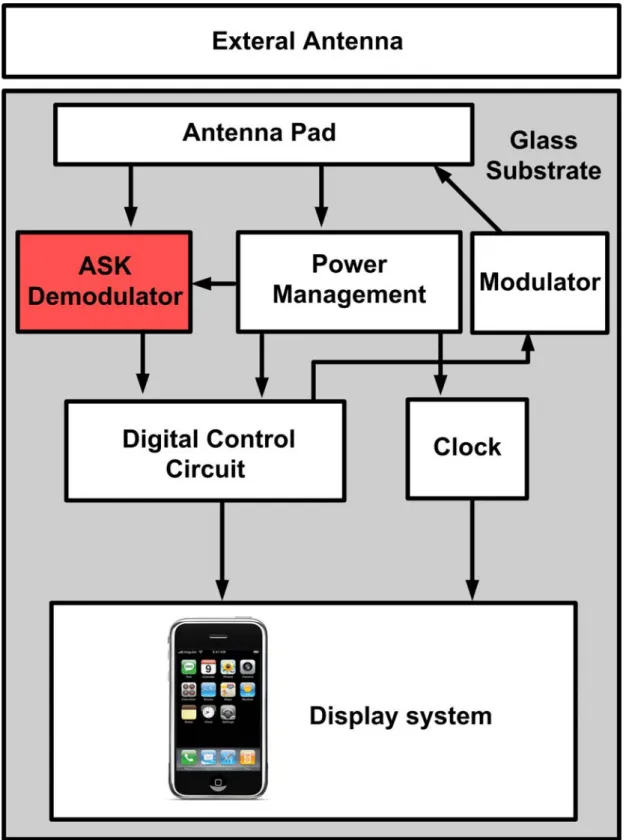
Fig. 1.5 is depicted the typical RFID system bolck for RFID tag in a portable device. The external antenna transmit raido frequency signals to RFID tag, the internal antenna receives the RF field and passes to analog block which composed of ASK demodulator, power management block, and modulator. The power management bolck provides stable voltage level and prevents overall system from destorying by ultra high voltage field inputting. The ASK demodulator alters the RF field to digital waveform in order to send logic signals to digital control block which regulates respondent information. The information is used by modulator changing to RF field to internal antenna and also controls the display system. Moreover, clock generator is also needed to supply reference clock to digital block.
ASK is one of the most popular modulation schemes for the RFID systems below 30 MHz. The conventional ASK demodulator can be realized by an envelope detector composed of a diode and low-pass filter,
as shown in Fig. 1.6, Xc(t) is the input ASK-modulated signal, and
ec(t) is the demodulated output signal. The input signal is first rectified and
the capacitor is charged to hold the envelope information. AS above description, the demodulator in tag will demodulated radio signals from the reader to digital data and synchronized clock, the digital data can be read
and write by decoder or memory, while the synchronized clock supplies their own digital circuit for operating.
1.2 Motivation
1.2.1 Improvement for memory in pixel circuits in high image
quality displays.
The memory-in-pixel (MIP) concept has attracted lots of interests for low power application [19], and it is proposed to implement a low power standby mode for continuous display of static images without the power wastage on the source drivers. By refreshing the voltage level of scan lines, polarity inversion can be easily produced even though the data is no longer furnished. So far, most of literatures have studied the digital MIP circuits [20]-[26]. They can be defined as two basic approaches: the first based on static type and the second based on dynamic type. In general, the static digital MIP circuit gives the lowest power consumption because dynamic power is only consumed when pixels are charged during polarity inversion. However, the main drawback of the static digital MIP is that it requires seven or eight TFTs and six row lines per pixel, which means it is typically too large for displays with a fine pixel pitch. Dynamic digital MIP circuits are attractive because of using fewer TFTs and row lines per pixel, but the theoretical power consumption is usually higher because a periodic refresh operation is required. In ref. [20], the dynamic digital MIP circuit can be
realized using just three n-type TFTs for one bit operation, as shown in Fig. 1.7. During the read period, selecting transistor series combines with a sensing transistor. The high or low impedance will be sensed on whether the pixel voltage is above or below the threshold voltage. Consequently, the final voltage on the column (high or low) is just the inverse of the pixel voltage. The inverted data is then written back onto the pixel. The refresh operation must be performed row by row and most power is consumed in pre-charging the columns.
For multi-bits application, static and dynamic digital MIP circuits still require suitable scan lines and capacitors to reach the action of polarity inversion, yet the adoption of analog concept for MIP circuit is attemptable since it can achieve higher image quality with fewer components. However, the analog memory circuit suffers an issue that the output voltage may have inaccuracy with corresponding data signal(a difference of the threshold voltage)or asymmetric inversion voltage(variation of threshold voltage), which means that the static image may be distorted with above errors. In this work, two types of analog pixel memory cells with the function of self voltage inversion for MIP application are proposed; moreover, the circuits is designed as solving the inaccuracy between input and output voltage and asymmetric inversion voltage.
1.2.2 RFID system on panel. (A-Si TFT ASK demodulator for
RFID tags.)
For conventional ASK demodulator, the high-frequency carrier is filtered out by the low-pass filter, but the charge and discharge cycles of the capacitor result in the ripples (Vripple) on the demodulated envelope. The
diode voltage drop (VD0) can debilitate the demodulated envelope. The
issue of voltage drop from diode becomes crucial when the input signal is weak and the ripple voltage is large. Therefore, Schottky diodes are preferred for the envelope detectors [27]. However, it requires an additional process cost to offer Schottky diodes so they may not be available in many Si-based semiconductor technologies. Since signal rectification is necessary for amplitude demodulation, the pn-junction diodes or diode-connected transistors are often used for implementing envelope detectors [28]–[30]. The voltage drops of the forward-biased diodes and diode-connected transistors may degrade the demodulator sensitivity.
Recently, full wave demodulator with LTPS TFT has been developed to resolve the issue of degrading sensitivity and reduce the ripples of the demodulated envelope [31], as shown in Fig. 1.8. However, followed by the tendency of TFT-LCD, low cost A-Si TFTs are still principal part for industry. So the most important issue is its low field-effect mobility (ability
to conduct current) and only one type(N-type transistor) transistor that cannot be used for complex circuits. In this work, a simplified full wave ASK demodulator of A-Si TFTs is proposed using one inverter and bootstrap transistor, high and low level digital data output with the analog RF field generating or not. Moreover, it is also designed for solving the degraded ripple and supplying higher voltage level output than original RF input.
Fig. 1.1 Pixel of liquid crystal display
Fig. 1.3 Basic concept of pixel memory technology
Fig. 1.6 conventional ASK demodulator and its waveform
Chapter 2
New proposed Analog Memory Cell (I) with Low
Temperature Polycrystalline Silicon TFTs
2.1 Device of LTPS TFTs
2.1.1 Structure of LTPS TFTs
Figure 2.1 shows the cross-sectional view of LTPS TFT technology [31]. Fabrication process starts from the buffer layer which was deposited on the glass substrate. Then, the undoped 50-nm-thick a-Si layer was deposited and crystallized by XeCl excimer laser with a laser energy density varied from 340mJ/cm2 to 420mJ/cm2. The recrystallized poly-Si films were patterned into the active islands. Afterward, a 60-nm-thick oxide layer was deposited as the gate insulator. Then, the 200-nm-thick molybdenum was deposited and patterned as the gate electrode. The n- doping was direct self-aligned to the gate electrode without additional mask process. The n+ source/drain regions were defined by one mask. The dopants were activated by thermal process. After the deposition of nitride passivation and the formation of contact holes, the 550-nm-thick titanium/aluminum/titanium tri-layer metal was deposited and patterned to
be the metal pads. For the analog pixel memory circuit verification, the channel length of all devices is kept as 5μm, while the channel width is varied from 30μm to 3μm in the circuit.
2.1.2 Measurement of LTPS TFTs
The LTPS TFTS is supported from AU Optronics Corporation, Hsinchu, Taiwan. For the methods of extraction the mobility and the threshold voltage are characterized, respectively.
Mobility
Generally, mobility can be extracted from the transconductancein gm
the linear region:
D O X D m D G V CONSTANT WC I g V V = L
μ
⎡∂ ⎤ =⎢ ⎥ = ∂ ⎣ ⎦ (2-1)Mobility can also be extracted from the slope of the curve of the square-root of drain current versus gate voltage in the saturation region,
i.e. For –VD > - (VG – VT)
(
)
2
D OX G THW
I
C
V
V
L
μ
=
−
(2-2) Threshold voltagePlenty of methods are available to determine Vth which is one of the
most important parameters of semiconductor devices. This thesis adopts the constant drain current method, which is, the voltage at a specific drain current NID is taken as Vth, that is, Vth = VG (NID) where Vth is threshold
voltage and NID stands for normalized drain current. Constant current
method is adopted in most studies of TFTs. It provides a Vth close to that
obtained by the complex linear extrapolation method. Generally, the threshold current NID = ID/(W/L) is specified at 10 nA in linear region and
at 100 nA in saturation region; W and L represent for TFT channel length and width, respectively.
Measurement results
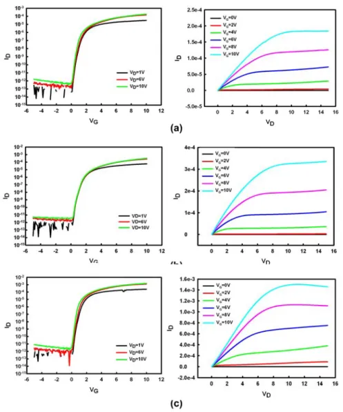
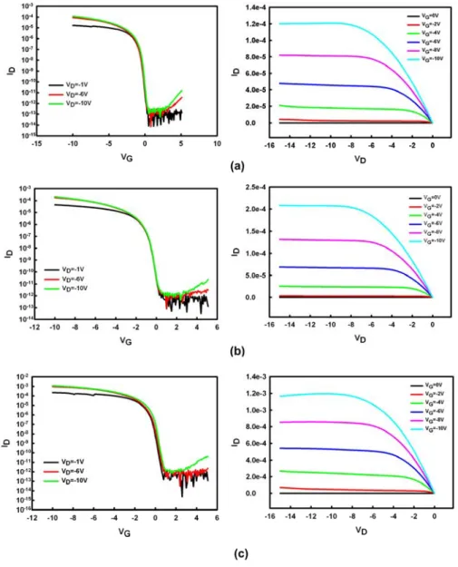
The measurement results are shown in Fig 2.2 and Fig 2.3 , using the above methods for extraction, the parameters for the size 3/5 , 5/5 and 30/5 (corresponding to the ratio of width to length: W/L) are shown in Table 2.1.
2.2 New proposed Analog Memory Cell (I)
2.2.1 Circuit Schematic and Operations
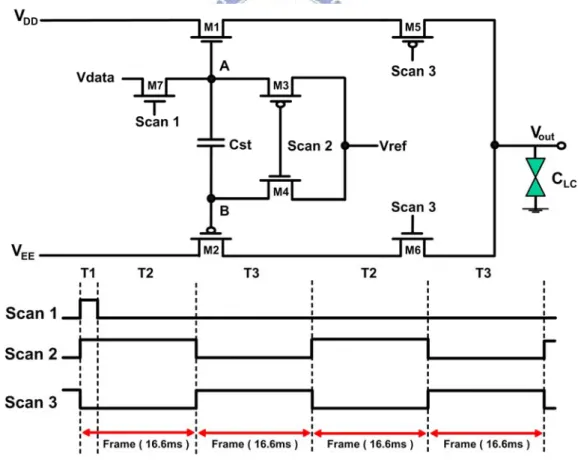
Fig. 2.4 shows the cooperation and connection block diagram between the proposed analog memory cell and the original pixel of LCD. During the standby mode for static image, the scan driver switches input from row signal (Row [N]) to control signals. Source driver provides Vdata (Vdata=|Vp|+|Vt|) to the data line where Vp is the original pixel data and Vt is the threshold voltage of Poly-Si TFT. Then, the analog memory cell samples Vdata and cooperates with control signals to supply the capacitive
loading (CLC) at Vout. Through this arrangement, the memory cell can self
generate inversion voltage for CLC. Therefore, the source driver can be
turned off at this duration until the specific frame is arrived. For example, if the frame time is 33.2ms, the source driver can be operated from 60Hz down to 30Hz for refreshing static image, compared to 16.6 ms of typical TFT-LCD frame time.
Fig. 2.5 depicts the proposed analog memory and the corresponding waveforms of scan lines. The proposed analog memory cell (I) is composed of two driving transistors (symbolized by M1 and M2), and five switch transistors denoted as (M3, M4, M5, M6, and M7). The operation is divided into three periods, including the data voltage pre-charging period (T1), positive voltage holding period (T2), and negative voltage holding period (T3). In the T1 period, Scan2 and Scan3 are set to turn off the transistors M3 and M6. The driving transistor M1 is operated as a source follower and Vout becomes Vdata–Vtn at the end of this period, where Vtn is the threshold voltage of M1. In the meanwhile, the storage capacitor (Cst) is set to the voltage of Vdata-Vref (where VA=Vdata and VB=Vref). In the
T2 period, Scan1 becomes low to turn off M7. Except for M7, other transistors are all kept at the previous states. The gate voltages of M1 and M2 are Vdata and Vref, respectively. Vout remains Vdata-Vtn at the positive data holding period (T2). At the T3 period, Scan2 and Scan3 are set to turn off M4 and M5. Because M3 is turned on, Vref is applied to the
node A. The voltage of node B goes to 2Vref-Vdata because Cst is boosted by the voltage at node A (VA). At the beginning of T3 period, M2 is
operated as a source follower and the output voltage goes to 2Vref-Vdata+|Vtp| and then holds this voltage level until the next period comes, where |Vtp| is the absolute threshold voltage of M2.
In the standby mode, Vout is varied by the M1 and M2 source followers, respectively. The threshold voltage difference between Vtn and |Vtp| will cause non-symmetric output waveforms, so liquid crystal can’t present equal transmittance. In order to solve this issue, it sets
Δ
V
=
Vtn
|
Vtp
|
, (1)and the request for negative data holding period (T3) is to generate opposite sign voltage (-Vout) during the positive data holding period (T2). Vout will become - (Vdata -Vtn), which gives
(Vdata Vtn)= VB+|Vtp|
= 2Vref Vdata+|Vtp|. (2)
Derived from Eq. (2), the optimized reference voltage (Vref) can be set to achieve the cancellation of threshold voltage difference between M1 and M2. The reference voltage is shown as followed
inversion voltage for analog MIP can be solved by this design method. This work develops a robust analog memory cell with the function of self voltage inversion, which requires fewer scan lines than conventional digital memory. Therefore, the proposed analog pixel memory cell is suitable for high resolution MIP application.
2.2.2 Simulation results
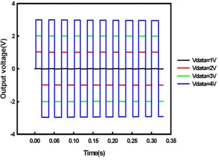
The proposed analog pixel memory circuit has been designed and verified by the HSPICE software with the RPI model (Level=62) in a 3-μm LTPS process. The aspect ratio of channel width (W) to channel length (L), W/L, for driving transistors M1 and M2 are 30μm/5μm, and those for switch transistors (M3, M4) and (M5, M6, M7) are 3μm/5μm and 5μm/5μm, respectively. Furthermore, the storage capacitor (Cst) is 5pF and the DC voltage supplies are 5V and -5V. Fig. 2.6 depicts the simulation results of the output (Vout) inversion voltage under Vdata inputs of 1V, 2V, 3V, and 4V, respectively. With the power saving concept, Fig. 2.6(a) shows twenty frame time (16.6ms×20=332ms) per Scan1 pulse which is equivalent to a frame rate of 3Hz for refreshing static image. The power consumption comes from source driver only when Vdata is sampled by the proposed analog memory cell. Afterward, the cell works between the positive and negative data holding periods to generate positive and negative pixel voltages at Vout only by the control signals. Fig. 2.6(a)
shows the output voltage is symmetric no matter how the input data changes. Besides, the high and low voltage level is decreased approximately a threshold voltage due to the operation of source followers.
Fig. 2.6(b) gives the partial enlarged plot of Fig. 2.6(a) when Vdata is 4V. After twenty frame time, the simulation result shows that the output voltage decay is only 0.05V. This represents the proposed circuit could be effectively operated higher than 5-bit (data range/one gray scale=3/0.05=60) digital memory at the frame rate of 3Hz.
2.2.3 Measurement setup
For measurement setup, synchronous signals are generated by pulse card of Keithly 4200-scs. Input range of Scan1 and (Scan2, Scan3) are set as 0V to 10V and -5V to 5V, respectively. Digital oscilloscope is utilized to observe output waveforms as shown in Fig .2.7. For circuit verification, twenty frame time per Scan1 is used to verify the output waveforms whether it could realize the design function.
2.2.4 Measurement result and discussions
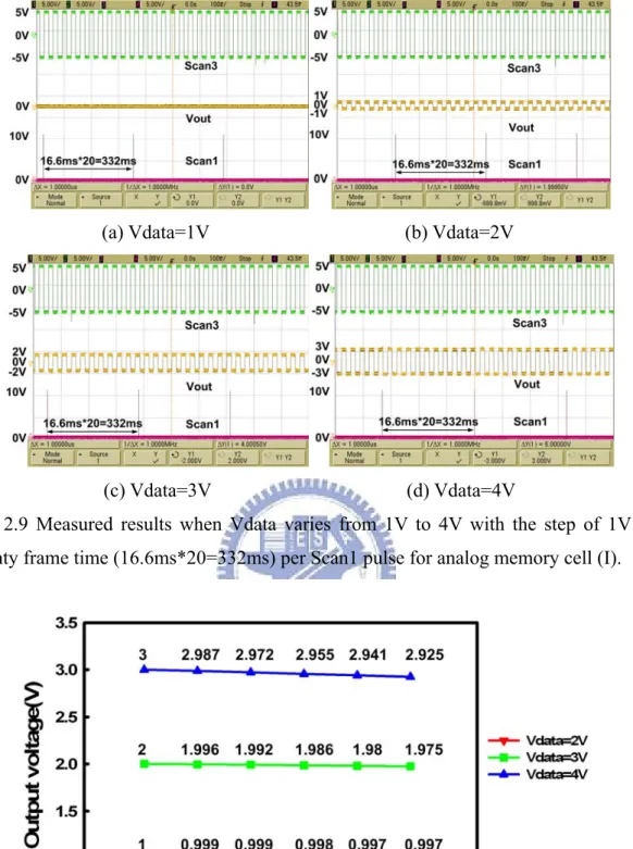
The die photo of fabricated two types of analog memory cells are shown in Fig. 2.8. A great part of the layout area is occupied by the storage capacitor (Cst) since it is fabricated by the interlayer oxide. The equivalent oxide thickness of the interlayer oxide is about eight times thicker than the gate oxide. In other words, storage capacitor can select gate oxide as an
alternative with restriction of the layout area. For circuit verification, using the above measurement setup, twenty frame time per Scan1 is used to verify the output waveforms whether it could realize the design function. As shown in Fig. 2.9 , the output inversion signal is from 0V to 0V, 1V to -0.998V, 2V to –2.015V, and 3V to -2.995V, when Vdata varies from 1V to 4V with the step of 1V and Vref is 0.2V (ΔV is about 0.4V). The inaccuracy for polarity inversion difference is no more than 0.025V because of Vref feeding. Fig. 2.10 shows the output voltage as a function of frame number with different values of Vdata. The maximum output voltage decay is less than 0.075V during twenty frame time when Vdata is 4V. It means that the operating frequency of source driver can be reduced from 60Hz to 3Hz for static image. Power consumption is reduced to about twenty times from the normal operation at standby mode. Besides, frame number can be chosen by the tolerance of specified output decay for higher resolution.
2.2.5 Summary
The Analog Memory Cell (I) with Low Temperature Polycrystalline Silicon TFTs is verified by SPICE simulation and measurement successfully. Using the reference voltage, the asymmetric inversion output voltage from the variation between threshold voltages of p-type and n-type is adjusted appropriately. Moreover, the circuit cell can reduce the
operating frequency of source driver from 60Hz to 3Hz in the standby mode, this means the power consumption is reduced effectively cause of decreasing frequencies of AC input data.
Fig 2-1. Cross-sectional view of LTPS TFT technology.
Fig 2-2. Diagram for N-type Poly-TFTs. (a)The ID-VG and IDVD of experiment results
for W/L=3um/5um. (b) The ID-VG and IDVD of experiment results for W/L=5um/5um.
Fig 2-3. Diagram for P-type Poly-TFTs. (a)The ID-VG and IDVD of experiment results
for W/L=3um/5um. (b) The ID-VG and IDVD of experiment results for W/L=5um/5um.
(C)The ID-VG and IDVD of experiment results for W/L=30um/5um.
Poly N-type TFT: Size(W/L): 3/5 5/5 30/5 Mobility(cm2/V.s) 44.55 43.5 40.325 Threshold voltage(V) 1.317 1.2 0.952 Poly P-type TFT: Size(W/L): 3/5 5/5 30/5 Mobility(cm2/V.s) 28.85 31.215 49.43 Threshold voltage(V) -0.938 -0.936 -0.345
Fig. 2.4 The block diagram of analog memory cell with the original pixel.
Fig. 2.5 Schematic of (a) the proposed memory cell (I) and (b) the corresponding control signals. The circuit is composed of two driving transistors (symbolized by M1 and M2) and five switch transistors denote as (M3, M4, M5, M6, and M7).
Fig. 2.6 The simulation results of output voltage for the proposed analog memory cell (I). (a) When Vdata is 1V, 2V, 3V, and 4V in twenty frame time per Scan1 pulse. (b) The partial enlarged plot of (a) when Vdata is 4V.
Fig. 2.7 The fabricated on-panel circuit for analog pixel memory and the corresponding measurement setup.
(a) b)
Fig. 2.8 The die photo of fabricated two types of analog memory cells. (a) Analog memory cell (I) and (b) analog memory cell (II).
(a) Vdata=1V (b) Vdata=2V
(c) Vdata=3V (d) Vdata=4V
Fig. 2.9 Measured results when Vdata varies from 1V to 4V with the step of 1V in twenty frame time (16.6ms*20=332ms) per Scan1 pulse for analog memory cell (I).
Fig. 2.10 The output voltage as a function of frame number with different values of Vdata for analog memory cell (I).
Chapter 3
New proposed Analog Memory Cell (II) with
Low Temperature Polycrystalline Silicon TFTs
for threshold voltage compensation
3.1 Circuit Schematic and Operations for threshold
voltage compensation
Fig. 3.1 depicts the proposed analog memory and the corresponding waveforms of scan lines. During the standby mode for static image, it samples Vdata and cooperates with scan lines to supply the capacitive loading (CLC) at Vout in Fig. 2.1. By applying the proposed circuit, source
driver need not provide Vdata as |Vp|+|Vt| to data line. It provides Vdata as |Vp| only. Therefore, source driver doesn’t have to modify the data signal with a threshold voltage shift and further decrease the algorithm complexity of source driver.
The proposed analog memory cell (II) is composed of two driving transistors (symbolized by M1 and M2), and seven switch transistors denoted as (M3, M4, M5, M6, M7, M8 and M9). The operation is divided into four periods, including the data voltage pre-charging period (T1), threshold voltage (Vt) generation period (T2), positive voltage holding period (T3), and negative voltage holding period (T4). In the T1 period, scan signals turn on the transistors (M4, M5, M7, M8 and M9) and turn off (M3 and M6), respectively. At this period, Vout becomes Vdata through
M9, and VA is charged to VDD. In the T2 period, Scan2 goes to high to turn
off M7. M1 starts to release charge from VA through diode connect
structure which becomes Vdata+Vtn at the end of this period, where Vtn is the threshold voltage of M1. In the meanwhile, the storage capacitor (Cst) is set to the voltage of Vdata+Vtn-Vref (where VA=Vdata+Vtn and
VB=Vref). In the T3 period, Scan1 becomes low to turn off M8 and M9.
Except for M8 and M9, other transistors are all kept at the previous states. The gate voltages of M1 and M2 are Vdata+Vtn and Vref, respectively. Vout remains Vdata at the positive data holding period (T3). At the T4 period, Scan3 becomes high to turn off M4 and M5. Because M3 is turned on, Vref is applied to the node A. The voltage of node B goes to 2Vref-(Vdata+Vtn) because Cst is boosted by the voltage at node A (VA).
At the beginning of T4 period, M2 is operated as a source follower and the output voltage goes to 2Vref-(Vdata+Vtn)+|Vtp| and then holds this voltage level until the next period comes, where |Vtp| is the absolute threshold voltage of M2.
Similar as the proposed analog memory cell (I), the threshold voltage difference between Vtn and |Vtp| will cause non-symmetric output waveforms, so that liquid crystal cannot present equal transmittance. In order to solve this issue, the request for negative data holding period (T4) is to generate opposite sign voltage (-Vout) during the positive data holding
|
Vtp
|
+
V
=
Vdata
B =2Vref (Vdata+Vtn)+|Vtp|. (4) Derived from Eq. (4), the optimized reference voltage (Vref) can be set to achieve the cancellation of threshold voltage difference between M1 and M2. The reference voltage is the same as Eq. (3). With adjusting this reference voltage, the problem of asymmetric inversion voltage for analog MIP can be also solved by the proposed analog memory cell (II).3.2 Simulation results
The aspect ratio of channel width (W) to channel length (L), W/L, for driving transistors M1 and M2 are 30μm/5μm, and those for switch transistors (M3, M4) and (M5, M6, M7, M8, M9) are 3μm/5μm and 5μm/5μm, respectively. Furthermore, the storage capacitor (Cst) is 5pF and the DC voltage supplies are 5V and -5V.
Fig. 3.2 depicts the simulation results of the output (Vout) under Vdata inputs of 1V, 2V, 3V, and 4V, respectively. The output voltage levels from Fig. 3.2(a) are the same as the input data. These results verify that the outputs are independent of threshold voltage from input data. Fig. 3.2(b) gives the partial enlarged plot of Fig. 3.2(a) when Vdata is 4V. After twenty frame time, the simulation result shows that the output voltage decay is only 0.06V. This represents the proposed circuit could be
effectively operated higher than 6-bit (data range/one gray scale=4/0.06=66.67) digital memory at the frame rate of 3Hz. Fig. 3.3 shows the output voltage (Vdata=3V) for M1 and M2 with equal threshold voltage shifts. In Fig. 3.3, there is no apparent difference between the absolute threshold voltages from 0.9V to 1.9V with the step of 0.5V. The error rates are just 1.14% and 2.12%, respectively. Therefore, these results show that the proposed analog memory cell (II) has higher reliability and more suitable for high resolution MIP application.
3.3 Measurement result and discussions
For the measurement setup, the Keithly 4200-scs and digital oscilloscope is utilized as well, only more one scan signal is added in the measurement. In Fig. 3.4 , the output inversion signal is from 1V to -0.998V, 2V to -2.015V, 3V to -3.015V, and 4.015V to -4.025V, when Vdata varies from 1V to 4V with the step of 1V and Vref is 0.2V (ΔV is about 0.4V). The inaccuracy for polarity inversion difference is no more than 0.015V. These results also show that the output voltage can directly obtain from Vdata without threshold voltage effects which are consistent with the simulation results. Furthermore, the maximum output voltage decay is less than 0.1V during twenty frame time when Vdata is 4V.
The reason for the voltage decay is caused by the parasitic effects of transistors. Take this part as an example, during the T3 and T4 alternative
parasitic capacitance and storage capacitor in Fig. 3.1(a). Because Vout is followed by VA and VB, the coupling voltage decay will directly affect
output voltage. For example, from positive data holding period changing to negative data holding period, the voltage at storage capacitor can be shown in the following [26] ( ) 4 2 2 Cgd C Cgs Vdata Vtn Vref Cgs C Vref V ST ST B + − + + + = . (5)
The second term of Eq. (5) is reduced because of capacitive voltage division, where Cgs2, Cgd2, and Cgs4 are the parasitic capacitance of M2 and M4. Moreover, this effect takes place at every transition of polarization inversion therefore leads to the output voltage decays since there is no refreshed data at the storage capacitor. In other words, after more frame periods, the holding voltage will be smaller than the previous one. In order to decrease the non-ideal effect, storage capacitor (Cst) has to be designed as large as possible to meet the ideal case in Eq. (4). However, it will limit the LCD’s aperture ratio. For measurement consideration, the capacitive ratio of oscilloscope and liquid crystal is about thirty times. The aspect ratio of M1 and M2 has to be designed larger (30μm/5μm). Therefore, larger storage capacitor (Cst=5pF) is needed to verify the functionality of the proposed circuit. Fig. 3.5 shows the output voltage as a function of frame number with different values of Vdata for analog memory cell (II). The maximum voltage decay value is 0.1V when Vdata is 4V. The frame
number can be chosen by the tolerance of specified output decay for higher resolution. By integrating the proposed MIP circuit on the pixel, better image quality and reliability can be obtained.
3.4 Summary
The proposed circuit with Low Temperature Polycrystalline Silicon TFTs for threshold voltage compensation is verified by SPICE simulation and measurement. The pixel memory cell can also reach 5 bit memory while the operation frequency of data driver is reduced to 3Hz, besides, the output inversion voltage is equal to the input data; that is, source driver doesn’t have to modify the data signal with a threshold voltage shift and further decrease the algorithm complexity of source driver.
(a)
(b)
Fig. 3.1 Schematic of (a) the proposed memory cell (II) and (b) the corresponding control signals. The circuit is composed of two driving transistors (symbolized by M1and M2) and seven switch transistors denote as (M3, M4, M5, M6, M7, M8 and M9).
(a)
(b)
Fig. 3.2 The simulation results of output voltage for the proposed analog memory cell (II). (a) When Vdata is 1V, 2V, 3V, and 4V in twenty frame time per Scan1 pulse. (b) The partial enlarged plot of (a) when Vdata is 4V.
Fig. 3.3 The output voltage for M1 and M2 with equal threshold voltage shifts from 0.9V to 1.9V with the step of 0.5V when Vdata is 3V.
(a) Vdata=1V (b) Vdata=2V
(c) Vdata=3V (d) Vdata=4V
Fig. 3.4 Measured results when Vdata varies from 1V to 4V with the step of 1V in twenty frame time (16.6ms*20=332ms) per Scan1 pulse for analog memory cell (II).
Fig. 3.5 The output voltage as a function of frame number with different values of Vdata for analog memory cell (II).
Chapter 4
New proposed radio frequency identification
demodulator circuit with Amorphous silicon
TFTS
4.1 Device of A-Si TFTs
4.1.1 Structure and Measurement of a-Si TFTs
The structure and the corresponding process follow and materials of a-Si TFT is shown in Fig 4.1. The properties of electrical device were measured by a Keithley 4200 IV analyzer in a light-isolated probe station at room temperature. In IDS-VGS measurement, the typical drain-to-source
bias was swept from VGS = -20 V to VGS = 20 V. In IDS-VDS measurement,
the typical drain-to-source bias was swept from VDS = 0 V to VDS = 20 V.
4.1.2 Parameter Extraction Method
In this session, we describe the methods of typical parameters extraction such as threshold voltage (Vth) and field effect mobility (μFE)
from device characteristics.
Threshold voltage (Vth) was defined from the gate to source voltage at
which carrier conduction happens in TFT channel. Vth is related to the gate
insulator thickness and the flat band voltage.
Plenty of methods are available to determine Vth which is one of the
most important parameters of semiconductor devices. This thesis adopts the method, which is, the intersection of and the extended line of
. Fig 4.1 is the example of this manner.
Determination of the Field-Effect Mobility
Typically, the field-effect mobility (μFE) is determined from the
transconductance (gm) at low drain bias (VD = 0.1 V). The TFT transfer
I-V characteristics can be expressed as
] 2 1 ) [( C μ = ID FE ox VG Vth VD VD2 L W − − (2-1) Where
COX is the gate oxide capacitance per unit area,
W is channel width,
L is channel length,
Vth is the threshold voltage.
Vth, the drain current can be approximated as: D th G V V V L W ) ( C μ = ID FE ox − (2-2)
The transconductance is defined as:
D V L W ox FE m =μ C g (2-3) Thus, m D OX g WV C L μFE = (2-4)
Similarly, we get mobility in the saturation region as
2 ( D) ox G L I WC V
μ
= ∂ ∂ (2-5)4.1.3 Model of a-Si TFTs
The models for simulation are implemented by a-Si TFTs. The extracted parameters are based on the device size of a-Si TFTs at 25℃. The field-effect mobility of a-Si TFTs is 0.369 cm2/V·s. The threshold voltage of a-Si TFTs is 4.019 V. In order to achieve higher accuracy of simulation result, we use different models to fitting corresponding width. Fig 4.2 shows the comparison fitting results between simulation and experiment which are very consistent. The parameters of spice models are demonstrated below:
*****************************************************
****** w=15 l=3 *******
.model NTFT15 NMOS (level=61 vto=-2.5 tox=4e-7
+ alphasat=0.775 gamma=0.68 kvt=-2.36 kasat=0.006 v0=0.11 rs=6000 rd=6000 vaa=710000
+ emu=1.56 sigma0=1e-13 el=0.035 vgsl=3.4 vdsl=7 iol=0.5e-13 vfb=-1 + delta=7 vmin=0.6 gmin=20e22 muband=0.036
+ m=4 lambda=1e-4 epsi=7.5 tnom=27) ******************************* ****** w=50 l=3 *******
.model NTFT50 NMOS (level=61 vto=-2.5 tox=4e-7
+ alphasat=0.775 gamma=0.68 kvt=-2.36 kasat=0.006 v0=0.11 rs=6000 rd=6000 vaa=710000
+ emu=1.56 sigma0=1e-13 el=0.035 vgsl=3.4 vdsl=7 iol=0.5e-13 vfb=-1 + delta=7 vmin=0.6 gmin=20e22 muband=0.035
+ m=4 lambda=1e-4 epsi=7.5 tnom=27) ******************************* ****** w=100 l=3 *******
.model NTFT100 NMOS (level=61 vto=-2.5 tox=4e-7
+ alphasat=0.875 gamma=0.68 kvt=-2.36 kasat=0.006 v0=0.11 rs=6000 rd=6000 vaa=710000
+ emu=1.56 sigma0=1e-13 el=0.035 vgsl=3.4 vdsl=7 iol=0.5e-13 vfb=-1 + delta=7 vmin=0.6 gmin=20e22 muband=0.034
+ m=4 lambda=1e-4 epsi=7.5 tnom=27) *******************************
****** w=200 l=3 *******
.model NTFT200 NMOS (level=61 vto=-2.5 tox=4e-7
+ alphasat=0.975 gamma=0.68 kvt=-2.36 kasat=0.006 v0=0.11 rs=6000 rd=6000 vaa=710000
+ emu=1.56 sigma0=1e-13 el=0.035 vgsl=3.4 vdsl=7 iol=1.5e-13 vfb=-0.8 + delta=7 vmin=0.6 gmin=20e22 muband=0.032
+ m=4 lambda=1e-4 epsi=7.5 tnom=27) ******************************* ****** w=500 l=3 *******
.model NTFT500 NMOS (level=61 vto=-2.5 tox=4e-7
+ alphasat=1.075 gamma=0.68 kvt=-2.36 kasat=0.006 v0=0.11 rs=6000 rd=6000 vaa=710000
+ emu=1.56 sigma0=1e-13 el=0.035 vgsl=3.4 vdsl=7 iol=3.0e-13 vfb=-0.3 + delta=7 vmin=0.6 gmin=20e22 muband=0.033
+ m=4 lambda=1e-4 epsi=7.5 tnom=27) ******************************* ****** w=1000 l=3 *******
.model NTFT1000 NMOS (level=61 vto=-2.5 tox=4e-7
+ alphasat=1.075 gamma=0.68 kvt=-2.36 kasat=0.006 v0=0.11 rs=6000 rd=6000 vaa=710000
+ emu=1.56 sigma0=1e-13 el=0.035 vgsl=3.4 vdsl=7 iol=5.0e-13 vfb=-0.3 + delta=7 vmin=0.6 gmin=20e22 muband=0.045
+ m=4 lambda=1e-4 epsi=7.5 tnom=27) ******************************* ****** w=2000 l=3 *******
.model NTFT2000 NMOS (level=61 vto=-2.5 tox=4e-7
+ alphasat=1.075 gamma=0.68 kvt=-2.36 kasat=0.006 v0=0.11 rs=6000 rd=6000 vaa=710000
+ emu=1.56 sigma0=1e-13 el=0.035 vgsl=3.4 vdsl=7 iol=4.0e-13 vfb=-0.3 + delta=7 vmin=0.6 gmin=20e22 muband=0.047
+ m=4 lambda=1e-4 epsi=7.5 tnom=27)
4.2 New A-Si RFID demodulator circuit
4.2.1Circuit Schematic and Operations
Fig 4.4 depicts the circuit schematic circuit and the corresponding input signals. The circuit is composed of two driving transistors(M1 and M2), one charged path(M3 and M4), a bootstrap capacitor, and a inverter block(M5~M7). When RF signals input (sine waveform), trnasistors M1 and M2 are turned on temporarily while the waveform is in low level. However, the input signal 1 and input signal2 are opposite signals that the transistor M1 and M2 are responsible for half time of charge transmitting. While in ths duration, voltage of node A (input of inverter) is discharged to low level (experimental input voltage is -15V), the output voltage follows the inverter is hold on high voltage level (VDD2=25V in experimental data). While RF field is broken off by transceiver, transistor M1 and M2 are turned off simultaneously, a charged path composed of M3 and M4 plays a role to determining the voltage of node A, parasistic capacitors
(Cgd1+Cgd2) which connected to node A is charged to VDD1 in this moment, while the ouput now is changed to low voltage level cause of input of inverter swithing.
However, the charged path always charged to node A no matter the RF field exists or not, so the size of transistor M1 and M2 are needed to design more larger that can be the predominant role when RF field exists. But when the the width of transistor M3 and M4 are designed small , the charging ability is not enough to lead the node A to high voltage level. Nevertheless, when the node A is charged, the voltage between gate and source of M4 is more and more small, by the typical driving formula(1) on saturation region of transistor, the charging current becomes smaller gradually. When it spends lots of time on node A charging, it also strongly influence the falling time of inverse output result.
2
)
(
2
1
t gs nV
V
L
W
Cox
u
I
=
−
(1)So the bootstrap capacitor is designed to solve the problem for driving capacity. While the voltage of node A(source of M3) is charged higher and higher, the node B(gate of M3) is also boots to higher; in other words, the current of M3 maintains stable when charging, the falling time of output is greatly reduced and good performance can reached by adding bootstrap installation.
voltage supply of inverter(VDD2), the digital signals can be high even if small RF field inputs. In other words, the voltage drop from input to output can be easily canceled in proposed demodulator. Moreover, using the full-wave demodulator(dual-RF signals input), the ripple for output is more smaller than the single input circuit.
4.2.2 Simulation results
The proposed A-Si RFID full wave demodulator circuit has been designed and verified by the HSPICE software with the model described in the preceding section. The simulated sizes of transistors are shown in Table 4.1. For driving transistors M1 and M2 are 2000um/3um, the M3 and M4 in charge path section are 100um/3um, the M5, M6, M7, and M8 are 100um/3um, 2000um/3um, 100um/3um, 1000um/3um. For voltage supply section, the sine input range is between -15V~15V with frequency 135KHz, voltage supply 1 is 15V, and the voltage 2 is 25. For the bootstrap capacitor is 5pF, and the loading resistance and capacitor is 5.2MΩ and 65pF.
The simulation result is shown in Fig.4.5, as the sine signals input, the demodulated output reach to high level voltage (22V~23V) even if the range of input voltage is only -15V~15V, the problem of voltage drop can be canceled by using the voltage supply of inverter bock, the low voltage level is about 1.66V, the rising time is 36us, while the falling time is 24us.
Since the charge path always exists, the rising time would larger than the falling time.
Fig 4.6 depicts the conventional half wave and full wave RFID demodulator circuit when using only N-type transistors. Diode connect transistor is regarded as a diode and the diode voltage drop equals to threshold voltage of transistor. Fig 4.7 and Fig 4.8 show the output waveform for these three circuits. The output of conventional demodulator are strongly influenced by the range of input data, since the diode voltage drop and a discharge path for connection with resistance, the output drop is about 6 to 7V. Moreover, cause of no enough discharging path existing, the falling time of conventional demodulator is extra higher than rising time. For the ripple when high voltage level holding, the full wave demodulator is almost half of the single wave one.
Table 4.2 depicted comparisons between conventional demodulator and proposed demodulator, the demodulated amplitude of proposed circuit is much larger than the conventional one, that is, the back-ends digital block in RFID tag can receive more accurate logic data, and the ripple voltage of proposed circuit is also better than the other two. However, as simulated result of Fig 4.9, adding the bootstrap capacitor lowering the falling time effectively, the falling time is shorter than other circuit about two orders.
4.2.3 Measurement setup
For measurement setup, synchronous signals are generated by pulse card of Keithly 4200-scs. Setting input range of signal 1 and signal 2 are -15V~15V, and the fabricated circuit on glass places on the probe card. The output waveform can be observed by oscilloscope, the equipments are shown in Fig 4.10.
4.2.4 Measurement result and discussions
For the measurement setup, the Keithly 4200-scs and digital oscilloscope is utilized as well, the output waveform is shown in Fig 4.11, the RF frequency of two inversion signals is 135KHz, and the operating period is set to 400us to observe. the output charges to 23.4V when the RF sine signals start to input and discharges to 1.1V after 200us while the RF field broke off.
Table 4.3 show that the similarity between the simulation result and the measurement, the difference for increasing of the falling time and decreasing of the rising time would impute to overestimating the charging path. Fig 4.12 shows the demodulated output when the input data range varies from -15V to 15V, -10V to 10V, -8V to 8V, and -5V~5V, the output
proposed circuit is about 8V. However, the proposed RFID full wave demodulator is succeed to demodulate RF field sine signals, and it also enlarges the voltage level of the input data to logic signals to ensure the accuracy for receiving.
4.2.5 Summary
The RFID full wave demodulator with Amorphous Silicon TFTs is verified by SPICE simulation and measurement successfully. Using the connection with two driving transistors, one charging path, and an inverter block, the demodulated output voltage from the RF field sine input is fit in with the simulation exactly. The operating frequency is 135KHz to 13.65MHz , and the demodulated amplitude is more than 100% compared with the input data, small ripple voltage and no voltage drop can easily and accurately transmit to the digital block in RFID tag.
Fig 4.2 Vth is the intersection of and the extended line of
Fig 4.4 Schematic of the proposed A-Si demodulator and the corresponding input signals. The circuit is composed of two driving transistors(M1 and M2), one charged path(M3 and M4), a bootstrap capacitor, and a inverter block(M5~M7).
Driving Transistor M1 M2 2000/3 2000/3 Charge path M3 M4 100/3 100/3 Inverter block M5 M6 M7 M8 100/3 2000/3 100/3 1000/3 Input range -15V~15V VDD1 15V VDD2 25V Cbootstrap 5PF
Table 4.1 The simulated value of transistor, capacitor, and voltage supply.
Fig 4.5 The simulated output for when sine input signals(-15V~15V), when RF field break off , the digital output changes from high level(1) to low level(0).
Fig 4.6 The conventional half wave (a) and full wave (b) RFID demodulator circuit when using only N-type transistors.
Fig 4.8 The output waveform between proposed ASKD demodulator and conventional full wave demodulator and corresponding ripple voltage.
Proposed demodulator Half wave conventional demodulator Full wave conventional demodulator Maximum voltage 23.7V 7.06V 8.05V Minimum voltage 1.65V 0.58V 0.66V
Rising time 36.2us 8.025us 3.98us Falling time 24.5us 301us 111us Ripple voltage 0.32 0.63 0.36 Table 4.2 The simulated result the three demodulator.