Ying Qian Wong, Hin Yong Wong, Ching Seong Tan, and Hsin-Fei Meng
Citation: AIP Advances 6, 125028 (2016); doi: 10.1063/1.4972202 View online: http://dx.doi.org/10.1063/1.4972202
View Table of Contents: http://aip.scitation.org/toc/adv/6/12
Published by the American Institute of Physics
Articles you may be interested in
Maxwell stress to explain the mechanism for the anisotropic expansion in lithiated silicon nanowires
AIP Advances 6, 125027125027 (2016); 10.1063/1.4972264
Vibrational mean free paths and thermal conductivity of amorphous silicon from non-equilibrium molecular dynamics simulations
AIP Advances 6, 121904121904 (2016); 10.1063/1.4968617
Enhanced temperature stability and quality factor with Hf substitution for Sn and MnO2 doping of (Ba0.97Ca0.03)(Ti0.96Sn0.04)O3 lead-free piezoelectric ceramics with high Curie temperature
AIP Advances 6, 125024125024 (2016); 10.1063/1.4972201
Stability, sub-gap current, 1/f-noise, and elemental depth profiling of annealed Al:Mn-AlOX-Al normal metal-insulator-superconducting tunnel junctions
AIP Advances 6, 125026125026 (2016); 10.1063/1.4972205
Low-energy SiC2H6+ and SiC3H9+ ion beam productions by the mass-selection of fragments produced from hexamethyldisilane for SiC film formations
AIP Advances 6, 125029125029 (2016); 10.1063/1.4972206
Band gaps in bubble phononic crystals
External serial connection without layer patterning
for organic solar cells
Ying Qian Wong,1Hin Yong Wong,1,aChing Seong Tan,1 and Hsin-Fei Meng2,a
1Faculty of Engineering, Multimedia University, Cyberjaya 63100, Malaysia 2Institute of Physics, National Chiao Tung University, Hsinchu 300, Taiwan
(Received 3 October 2016; accepted 29 November 2016; published online 16 December 2016)
This paper proposes a novel alternative to conventional internal serial connec-tion, where precise patterning and scribing of organic layers can be eliminated. Adjacent cells can be made nearer for better space-utilization and higher volt-ages per unit area. Also, blade coating is proposed as the fabrication method as it has low material wastage (less than 5%), easily scalable to large area, has high film uniformity and has high throughput due to its roll-to-roll potential. This paper demonstrates 3-cells large area (12.98 cm2) external serial connection organic solar cells (OSCs) using the material poly(3-hexylthiophene-2,5-diyl) : [6,6]-phenyl-C61-butyric acid methyl ester (P3HT:PCBM) and 2,6-Bis(trimethyltin)-4, 8-bis(5-(2-ethylhexyl)thiophen-2-yl)benzo [1,2-b : 2,6-Bis(trimethyltin)-4,5-b0]dithiophene:6,6-phenyl C71-butyric acid methyl ester (PBDTTT-CT:PC71BM) respectively. The power conversion efficiencies (PCEs) of the resulting 3-cells modules are 2.0% and 4.1% respectively. © 2016 Author(s). All article content, except where other-wise noted, is licensed under a Creative Commons Attribution (CC BY) license (http://creativecommons.org/licenses/by/4.0/). [http://dx.doi.org/10.1063/1.4972202]
I. INTRODUCTION
The ultimate objectives of solar research are to achieve a truly low-cost, scalable to large area, high throughput, and highly efficient solar cell. Therefore, the materials used should be of low-cost and the manufacturing methods should be kept simple with no high temperature processes involved. Organic Solar Cell (OSC) deposited using blade coating technology potentially realizes these. Blade coating has low material wastage (less than 5%), easily scalable to large area, has high film uniformity and has high throughput due to its roll-to-roll potential.1In addition to that, the amount of the material required for blade coating is 20% of that required for spin coating, which means that the cost of fabrication using blade coating can be greatly reduced. Together, these made the low-cost fabrication of large-area integrated devices possible.
To-date, the highest reported power conversion efficiency (PCE) of OSCs is 11.5% by Yan et al.2 However, this PCE is for single-junction cell where the voltage is less than 1.0 V. The upscaling of OSCs from laboratory design to practical cells that deliver appreciable electrical power is as important as achieving high PCE because most applications require higher voltages than the typical OSCs’ voltage of around 0.5 V. Higher voltages can be achieved by connecting OSCs in series to increase produced voltages.3 Yoo et al. demonstrated that the open-circuit voltage (VOC) scaled linearly with the number of OSC connected in series. For example, if the number of OSC connected in series is 3, VOC= 3 x 0.621 V.4
Several groups have demonstrated different methods to achieve serial connection OSCs but the designs mostly revolved around the structure investigated by Lungenschmied et al, as shown in Fig.1. Note that this type of serial connection is referred as internal serial connection in this paper as the connection between each cell is done within/near the active area. PCE is inversely proportional to
aCorresponding authors. Email addresses:[email protected](H. Y. Wong),[email protected](H.-F. Meng).
FIG. 1. Internal serial connection OSC with three cells.3
the width of the electrode. The PCE decreased by about 85% when the width of the electrode was increased from 1 cm to 10 cm. Thus, the dimensions of the electrodes are crucial in designing serial connection OSCs. In order to have high PCE serial connection OSCs, the electrodes have to be in the form of narrow strips and must have contacts on the long sides to minimize resistive losses. This is to ensure charge carriers travel only a minimum distance in the resistive indium tin oxide (ITO) electrodes.3
Other than the dimension of the electrodes, the connections of the cathode of one cell to the anode of the next cell also play a very important role in minimizing surface area losses. With respect to the cell width, the distance between adjacent solar cells has to be as small as possible in order to minimize the reduction of PCE. The electrode strips have to be precisely aligned and size perfectly controlled.5 In addition to that, the other layers on top of the anode, such as the hole transport layer, active layer, electron transport layer and cathode require patterning to achieve series connections.
These layer patterning can be achieved by few methods such as laser scribing,5,12mechanical scribing6–9 and silk screen printing.10,11 However, these methods have their own limitations. For laser scribing, the underlying layers are prone to damages and large amounts of debris are produced next to the structured line. This could result in shunting of adjacent cell.13For mechanical scribing, there are limitations in terms of scribe widths and accuracy.14There are risks of contaminating the substrate with particles and the limitation of applying this method on flexible substrates as well.9 As for silk screen printing, this method requires high viscosity solution (50-50000 mP·s) whereas organic solutions are normally of low viscosity (1-5 mP·s).15In addition, all these layer patterning methods have to be precise without compromising device performance because when connected in series, the current goes through every component in the device. If there are cell-to-cell variations, the short-circuit current (ISC) will be limited by the cell producing the smallest photocurrent.4Thus every cell must function well in order to achieve high performance serial connection OSC. At the same time, the precise layer patterning technology has to be low-cost as the aim is to achieve a low-cost OSC feasible for commercialization.
In this study, a novel method to achieve serial connection OSCs is proposed. This method does not require precise patterning and does not involve significant increase in cost. This serial connection method is referred as external serial connection because the connection from one cell to the next is accomplished outside the active area. The other methods reported by other authors3,5–12are considered as internal serial connection as the connection is done within/near the active area.
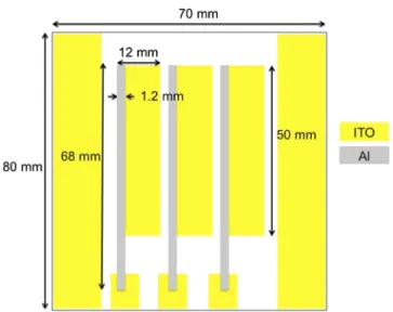
In this work, the ITO-coated substrate for both the internal serial connection and exter-nal serial connection are exactly the same except for the exterexter-nal serial connection substrate, there are additional narrow strip of AE on each of the ITO cell and at the bottom of the sub-strate, there are additional ITO squares which serve as a platform for characterizing each cell even after encapsulation. This design enables convenient debugging. The internal serial con-nection and external serial concon-nection are illustrated in Fig. 2 and Fig. 3 respectively. For the internal serial connection, the distance between adjacent solar cells is 5 mm whereas the cell width is 9 mm. For the external serial connection, the distance between adjacent solar cells is 4 mm and the cell width is 10 mm. Note that this work aims for external serial connection feasibility testing. There are more factors to consider in order to be fully practical and this will be discussed in the future work section.
FIG. 2. Internal Serial connection OSC with three cells (a) Top view of ITO-coated substrate (b) Top view of all layers (black dashed line as cross-section for Side View) (c) Cross-section side view (Note: Encapsulation glass is not shown in the cross-section side view and the figures are not drawn to scale. It is for illustration purposes only).
For initial testing, poly(3-hexylthiophene-2,5-diyl) : [6,6]-phenyl-C61-butyric acid methyl ester (P3HT:PCBM) was used as the active layer. This is because this blend of material is well-established. This could reduce any material uncertainties while investigating the external serial connection feasibility. Using the best experimental conditions achieved for P3HT:PCBM,
FIG. 3. External Serial connection OSC with three cells (a) Top view of ITO-coated substrate with narrow strip of assisting electrode (AE) and bottom ITO squares for cell characterization (b) Top view of all layers (black dashed line as cross-section for Side View) (c) Cross-section side view (Note: Encapsulation glass is not shown in the cross-section side view and the figures are not drawn to scale. It is for illustration purposes only).
another blend of low bandgap polymer and fullerene, namely 2,6-Bis(trimethyltin)-4,8-bis(5-(2-ethylhexyl)thiophen-2-yl)benzo[1,2-b : 4,5-b0]dithiophene:6,6-phenyl C71-butyric acid methyl ester
(PBDTTT-CT:PC71BM) was also used to demonstrate the external connection. Their performances are on par with the internally-connected modules and they will be discussed in Results and Discussions.
II. EXPERIMENTAL DETAILS
In this investigation, the bulk-heterojunction consisting of P3HT as the electron donor and PCBM as the electron acceptor were used initially. The device structure was ITO/Al/PEDOT:PSS (40 nm)/P3HT:PCBM (200 nm)/LiF (0.8 nm)/Al. For comparison purposes, an internal serial con-nection device was fabricated. The device structure was the same with the exception for aluminium (Al) assisting electrode (AE) that was not necessary in internal serial connection. The AE in external serial connection serves to reduce the series resistance (Rs) of the ITO anode and to extend the anode connection to a region outside of the active area.
Initially, the 7 cm x 8 cm prepatterned ITO-coated glass substrates were treated with deter-gent in an ultrasonic bath for 15 min. Then, they were rinsed three times with deionized water (DI water). Using a shadow mask, narrow strips of Al assisting electrode (AE) with the width of 0.6 mm were thermally evaporated in a vacuum chamber with a base pressure below 3.0 x 10⁻⁶ Torr onto the ITO anode. The thickness of the AE was varied between 100 nm to 400 nm for different sets of experiments. When fabricating for internal serial connection device, this step was skipped. Next, they were exposed under an ultraviolet (UV) ozone cleaner for another 15 min. Then, 100 µL of [poly-(3,4-ethylenedioxythiophene):poly-(styrenesulfonate) (PEDOT:PSS) (CLEVIOSTM P VP AI4083) was deposited onto the blade gap of 60 µL and it was blade-coated at 20 mm/s at 60◦C onto the substrate to form a 40 nm thick hole-transport layer. PEDOT:PSS in water solution from 1.3 wt. % to 1.7 wt. % was first diluted by Isopropanol (IPA) in a 1:2 volume ratio before blade coating. Without dilution, the resulting thickness will be too large. During the blade coating process, hot air was simultaneously applied from the top using a blower with a diffusing showerhead to enhance the drying speed and uniformity. After blade coating, the films were baked at 150◦C for 15 minutes.
Subsequently, 50 µL of P3HT:PCBM in chlorobenzene was deposited onto the blade gap of 60 µL and it was blade-coated at a speed of 200 mm/s at 80◦C onto the substrate to form a 200 nm thick BHJ layer. In this step, hot air was applied from the top as well. P3HT (purchased from Rieke Metals, Inc.) and PCBM powders (purchased from Nano-C, Inc.) were mixed one day before and was dissolved at 80◦C using the solvent chlorobenzene in a 20 mg:20 mg:1110 mg weight ratio. For the internal serial connection, mechanical scribing as described in Ref.6was employed at this step, as it is necessary to expose the ITO of the next cell in order to form series connection. For external serial connection, scribing was not necessary. Thus, the substrates were immediately subjected to thermal annealing at 140◦C for 20 minutes after coating the active layer. Next, using a shadow mask, LiF (0.8 nm)/Al was thermally evaporated in the vacuum chamber with the base pressure below 3.0 x 10⁻⁶Torr as well. The thickness of the Al cathode was also varied between 100 nm to 200 nm for different sets of experiments. Finally, the samples were encapsulated in order to prevent oxygen and moisture ingress before characterizations.
As for the fabrication of the 3-cells module using the material PBDTTT-CT:PC71BM, the fab-rications procedures were exactly the same with P3HT:PCBM, except for the solution preparation and the blade coating parameters. For solution preparation, PBDTTT-CT (purchased from Solarmer Materials Inc.) and PC71BM powders (purchased Solenne) were mixed one day before and was dis-solved at 80◦C using the solvent toluene in a 10 mg:15 mg:867 mg weight ratio. For the deposition of the active material, 90 µL of PBDTTT-CT:PC71BM in toluene was deposited onto the blade gap of 60 µL and it was blade-coated at a speed of 30 mm/s and an acceleration of 15 mm/s2at 80◦C onto the substrate to form a 100 nm thick BHJ layer. In this step, hot air was applied from the top as well. After that, the electrodes were thermally evaporated as the P3HT:PCBM.
The current density-voltage (J-V) characteristics were measured using a Keithley 2400 source measurement unit and the PCE of the devices were measured using a 100 mW/cm2AM 1.5G solar simulator. In order to obtain an accurate PCE calculation, the active area of the devices, which were 0.9 cm x 4 cm x 3 cells = 10.8 cm2for internal serial connection and 1 cm x 4 cm x 3 cells = 12 cm2
for external serial connection were taken into account. For the optimized wide cathode external serial connection type (this will be discussed in the next section), there was an additional area of 0.7 cm x 0.7 cm x 2, thus the total active area was 12.98 cm2. As for the film thickness, a 3D profiler and surface roughness measurement instrument, Kosaka ET200 was employed.
III. RESULTS AND DISCUSSIONS
In order to compare the performance between internal serial connection and external serial con-nection, an internal serial connection device having the structure ITO/PEDOT:PSS (40 nm)/P3HT: PCBM (200 nm)/LiF (0.8 nm)/Al (100 nm) was fabricated. The PCE for this device was 2.4%, with JSC = 2.5 mA/cm2, VOC = 1.87 V and FF = 0.51. Comparing with the external serial connection device with an AE thickness of 100 nm and cathode thickness of 100 nm, the external serial con-nection device showed rather poor performance with PCE = 0.6%, with JSC = 1.3 mA/cm2, VOC = 1.84 V and FF = 0.27. This was expected as the electrode design for the internal serial con-nection device was optimized to have short travel distance for the charge carriers. Since scribing was involved to expose the ITO of the next cell, the charge carriers only had to travel around 1 cm to achieve series connection. Whereas for the external serial connection device, it was designed in such a way where the tedious scribing step was not necessary, rather the series con-nection was achieved outside of the blade coating area. The charge carrier had to travel through a highly resistive and longer pathway of around 4 cm to achieve series connection with the next cell.
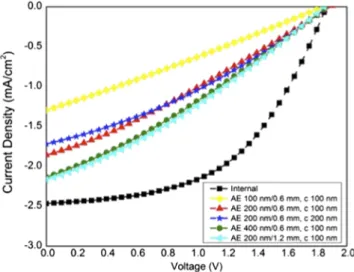
As shown in Fig.4, the poor performance of the device was due to its highly resistive nature. It had high series resistance (Rs) and low shunt resistance (Rsh). Rs and Rshcan be estimated from the inverse slope of the J-V curve near the open-circuit voltage point and the inverse slope of the J-V curve near the short-circuit current point respectively. When Rs is significantly high, the J-V curve would appear similar to that of cell with low Rsh. The JSCwas reduced significantly, to about half the value of the internal serial connection device. Since the narrow cathode connection parts, as highlighted by the circles in Fig.3(b)for the external-serial connection, act as localized high Rs area, this trend in the J-V curve was expected. Therefore, the design optimization aimed to reduce the series resistance of the longer pathway.
Since resistance is determined by the material’s resistivity ( ρ), length (`) and cross-sectional area (A), as shown in (1), we investigated if increasing the thickness of AE and cathode could reduce its Rs to be at least similar or at least on par with the internal serial connection device. The cross-sectional
FIG. 4. Measured illuminated J-V curves for P3HT:PCBM for internal serial connection and external serial connection with narrow cathode connection. Different assisting electrode (AE) thickness/width and different cathode (c) thickness were investigated.
FIG. 5. Top view of ITO-coated substrate with wider strip (1.2 mm) of assisting electrode (AE) for External Serial connection OSC with three cells.
area is a product of the width (ω) and thickness (t) of the material. R= ρ `
ωt (1)
The thickness of AE was first increased to 200 nm. There was a significant improvement especially in terms of JSC. It increased from 1.3 mA/cm2to 1.9 mA/cm2. As a result, the PCE was shown to increase from 0.6% to 1.0%. From Fig.4, the J-V curve for this device clearly showed lower Rscompared to the previous device. Since the performance for external serial connection was still significantly lower than the performance for internal serial connection, the cathode thickness was increased to 200 nm as well. This did not show much improvement. It was suspected that this was due to significantly high localized Rsin the narrow cathode connections, where even increasing the thickness of the cathode was not sufficient to reduce its total Rs to show any performance improvement. Therefore, while maintaining the cathode thickness at 100 nm, the AE thickness was increased to 400 nm. JSC did increase from 1.9 mA/cm2to 2.1 mA/cm2. Increasing the thickness of AE showed more significant improvement in terms of JSC compared to increasing the thickness of the cathode. This might be attributed to the highly resistive nature of ITO. Since the AE was in contact with the highly resistive
FIG. 6. External Serial connection OSC with three cells with wider cathode connections (Note: Figures are not drawn to scale. It is for illustration purposes only).
FIG. 7. Measured illuminated J-V curves for P3HT:PCBM for internal serial connection and external serial connection with wide cathode connection. Different assisting electrode (AE) thickness/width and cathode (c) thickness were investigated.
ITO, increasing the thickness of AE helped to reduce the ITO’s resistance and therefore, it facilitated in charge transport.
On the other hand, since cross-sectional area is a product of width and thickness, the width of AE was also expanded by two times to reduce the resistance. It was expanded from 0.6 mm, as shown in Fig.3(a)to 1.2 mm, as shown in Fig.5. The device showed increment in terms of JSC. It recorded a value of 2.2 mA/cm2 and thus resulting in a PCE of 1.2%. Nevertheless, the FF value was still significantly low compared to the internal serial connection device. The previous efforts on increasing the thickness of AE and cathode only affected the JSCvalue. Therefore, further optimization was required in order to boost its performance to be as close to internal series connection as possible. Since the thickness increment of the AE and cathode was in the order of nanometers, the reduction in resistance was not significant. Therefore, a new shadow mask for cathode was designed. Changes were made to the narrow cathode connection parts, as highlighted by the circles in Fig. 3(b). By making the cathode connection wider, as shown in Fig.6, the cross-sectional area was increased in the order of millimeters. It was anticipated that this would result in a significant reduction in resistance, hence an increase in FF, and eventually in PCE itself. At first, the performance was still poor as the FF remained at 0.33 and PCE was only 1.2% with AE thickness of 200 nm, AE width of 0.6 mm and cathode thickness of 100 nm. However, while maintaining the same AE and cathode thickness, a significant improvement was obtained when the AE was again made twice wider (1.2 mm). Together with the wider cathode connections, the PCE rose to 2.0%, with JSC= 2.5 mA/cm2, VOC= 1.81 V and FF = 0.44. Improvements were seen in both JSCand FF. The J-V curves are shown in
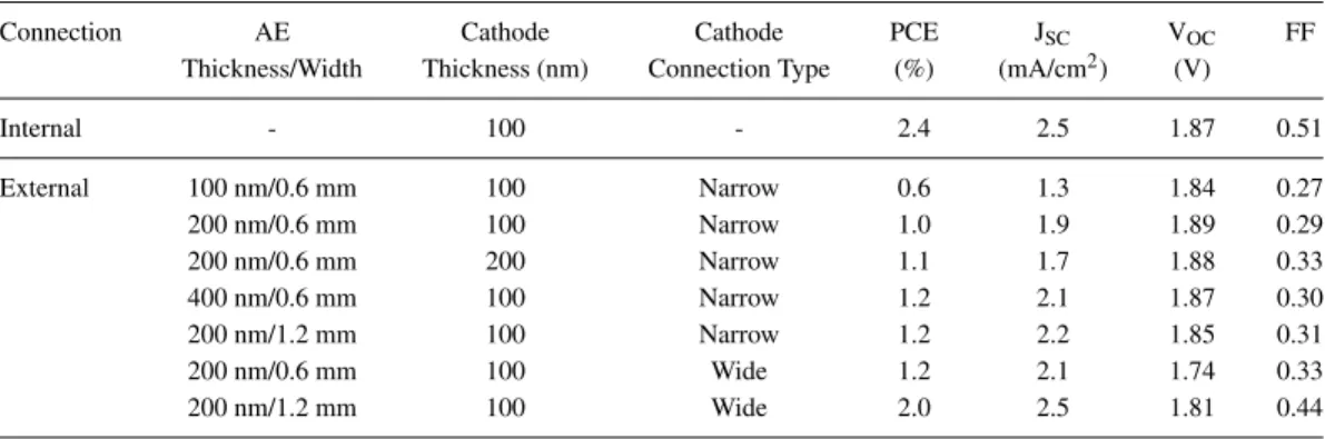
TABLE I. Performance Comparison between Internal and External Serial Connection for P3HT:PCBM.
Connection AE Cathode Cathode PCE JSC VOC FF
Thickness/Width Thickness (nm) Connection Type (%) (mA/cm2) (V)
Internal - 100 - 2.4 2.5 1.87 0.51 External 100 nm/0.6 mm 100 Narrow 0.6 1.3 1.84 0.27 200 nm/0.6 mm 100 Narrow 1.0 1.9 1.89 0.29 200 nm/0.6 mm 200 Narrow 1.1 1.7 1.88 0.33 400 nm/0.6 mm 100 Narrow 1.2 2.1 1.87 0.30 200 nm/1.2 mm 100 Narrow 1.2 2.2 1.85 0.31 200 nm/0.6 mm 100 Wide 1.2 2.1 1.74 0.33 200 nm/1.2 mm 100 Wide 2.0 2.5 1.81 0.44
FIG. 8. Fabricated P3HT:PCBM devices (a) Internal Serial Connection (b) External Serial Connection with narrow cathode connection (c) External Serial Connection with wide AE and wide cathode connection (Note: ITO of the devices are facing up).
TABLE II. Performance Comparison between Internal and External Serial Connection for PBDTTT-CT:PC71BM.
Connection AE Cathode Cathode PCE JSC VOC FF
Thickness/Width Thickness (nm) Connection Type (%) (mA/cm2) (V)
Internal - 100 - 4.2 4.0 2.51 0.55
External 200 nm/1.2 mm 100 Wide 4.1 3.9 2.43 0.43
Fig.7. This was an interesting finding as making the AE wider without the wider cathode connection or maintaining narrow AE but with the wider cathode connection did not result in any improvement. It was only when both the wide AE and the wide cathode connection were used, the device showed significant improvement. This indicated that the Rson both the AE and the cathode had to be low in order to increase FF. The charge carriers travel easier from the wide cathode connection to the wide AE of another cell to form a smooth external series connection. The results are all compiled in TableI. The fabricated devices of internal serial connection, external serial connection using narrow cathode connection and wide cathode connection are shown in Fig.8(a),(b)and(c)respectively.
Since the external connection design was proven to be feasible using P3HT:PCBM, another module using the material PBDTTT-CT:PC71BM was fabricated. Both the internal serial connection and external serial connection were fabricated for comparison. For the internal serial connection module, the PCE device was 4.2%, with JSC= 4.0 mA/cm2, VOC= 2.51 V and FF = 0.55. Comparing with the external serial connection device with an AE thickness of 200 nm, width of 1.2 mm and cathode thickness of 100 nm, the external serial connection device showed similar performance with PCE = 4.1%, with JSC= 3.9 mA/cm2, VOC= 2.43 V and FF = 0.43. These results are compiled in TableII.
IV. CONCLUSIONS AND FUTURE WORK
In summary, the serial connection large-area OSCs, achieved through external serial connection, where layer patterning is not necessary, was successfully demonstrated. Adjacent cells can be made nearer for better space-utilization and higher voltages per unit area. For a 3-cells P3HT:PCBM device, a PCE of 2.0% was obtained. As for a 3-cells PBDTTT-CT:PC71BM, a PCE of 4.1% was obtained. The PCEs were as good as the internal serial connection modules. The present study results highlight the importance of the geometry of the AE and the cathode in order to have good JSC and FF. For future work, uniform thickness for every layer throughout the whole substrate, smaller gap between each cell for area optimization and better cathode connection design are desired. The gap could be as small as possible where the limitation is dependent on the photoligraphy technique, since layer patterning is not necessary for external serial connection. It is believed that this would increase the overall performance of the device, even better than the internal connection module. To further reduce the cost and time induce by the thermal evaporation of AE, graphene could be used to replace the both the ITO and the strip of AE as graphene has high conductivity and has proven to be suitable for electrode application.16 The external serial connection may be a promising alternative for the fabrication of low-cost, large area and high throughput solar cell.
ACKNOWLEDGMENTS
The authors gratefully acknowledge Motorola Foundation, Malaysia for the financial support through the grant no. EP20121123003. We also acknowledge the NCTU Taiwan Elite Internship Program for providing the opportunity for research collaborations between MMU and NCTU. Y. Q. Wong would like to thank Prof. H.-F. Meng for providing his laboratory to work on this research. This work was supported by the National Science Council (NSC) of Taiwan, under grant NSC104-2119-M- 009-012-. We also acknowledge P.-T. Tsai and C.-Y. Wu for the experimental support and helpful discussions.
1S. L. Lim, E.-C. Chen, C.-Y. Chen, K.-H. Ong, Z.-K. Chen, and H.-F. Meng, “High performance organicphotovoltaic cells
2National Renewable Energy Laboratory (NREL), in Best Research-Cell Efficiencies, Jan. 11, 2016. [Online]. Available:
http://www.nrel.gov/ncpv.
3C. Lungenschmied, G. Dennler, H. Neugebauer, S. N. Sariciftci, M. Glatthaar, T. Meyer, and A. Meyer, “Flexible, long-lived,
large-area, organic solar cells,”Solar Energy Materials and Solar Cells91(5), 379–384 (2007).
4S. Yoo, W. J. Potscavage, B. Domercq, J. Kim, J. Holt, and B. Kippelen, “Integrated organic photovoltaic modules with a
scalable voltage output,”Applied Physics Letters89, 1–3 (2006).
5G. Dennler, C. Lungenschemied, H. Neugebauer, N. S. Sariciftci, and A. Labouret, “Flexible, conjugated, polymer-
fullerene-based bulk heterojunction solar cells - basics, encapsulation and integration,”Journal of Materials Research20(12), 3224–3233 (2005).
6P. T. Tsai, K.-C. Yu, C.-Y. Chang, S.-F. Horng, and H.-F. Meng, “Large-area organic solar cells by accelerated blade coating,”
Organic Electronics22, 166–172 (2015).
7R. Gehlhaar, D. Cheyns, L. Van Willigenburg, A. Hadipour, J. Gilot, R. Radbeh, and T. Aernouts, “Four-terminal organic
solar cell modules with increased annual energy yield,” Organic Electronics 8830, 883001-1–883001-13 (2015).
8B. Muhsin, J. Renz, K. H. Drue, G. Gobsch, and H. Hoppe, “Efficient polymer solar cell modules,”International Conference
on Science and Technology of Synthetic Metals159, 2358–2361 (2009).
9M. Niggemann, B. Zimmermann, J. Haschke, M. Glatthaar, and A. Gombert, “Organic solar cell modules for specific
applications from energy autonomous systems to large area photovoltaics,”Thin Solid Films516, 7181–7187 (2008).
10F. C. Krebs, J. Alstrup, H. Spanggaard, K. Larsen, and E. Kold, “Production of large-area polymer solar cells by industrial
silk screen printing, lifetime considerations and lamination with polyethyleneterephthalate,”Solar Energy Materials and Solar Cells83(2-3), 293–300 (2004).
11F. C. Krebs, “Polymer solar cell modules prepared using roll-to-roll methods: Knife-over-edge coating, slot-die coating and
screen printing,”Solar Energy Materials and Solar Cells93, 465–475 (2009).
12R. Tipnis, J. Bernkpof, S. Jia, J. Krieg, S. Li, M. Storch, and D. Laird, “Large-area organic photovoltaic module- fabrication
and performance,”Solar Energy Materials and Solar Cells93, 442–446 (2009).
13B. P. Randand and H. Richter, “Module design, fabrication, and characterisation,” Organic Solar Cells: Fundamentals,
Devices, and Upscaling, chapter 14 (2014), pp. 663–712.
14M. W. Rowell and M. D. McGehee, “Transparent electrode requirements for thin film solar cell modules,”Energy &
Environmental Science4, 131 (2011).
15Y. Galagan and R. Andriessen, “Organic photovoltaics: Technologies and manufacturing,”Third Generation Photovoltaics
61–91 (2012).
16H. Park, S. Chang, M. Smith, S. Gradeˇcak, and J. Kong, “Interface engineering of graphene for universal applications as