quency acquisition is assisted by received signal strength indicator (RSSI) for automatic frequency sweeping and fast locking. Fabri-cated in 65 nm CMOS technology, the chip size is 0.92 . The PLL locking time is less than 3 . This chip drains 24 mW from a 1.2 V power supply.
Index Terms—Harmonic mixer, PLL, RSSI, tripler. I. INTRODUCTION
C
MOS Terahertz (THz) systems are considered as emerging technology for advanced imaging and spectroscopy for sensing and detection applications, and have drawn tremen-dous research efforts recently [1], [2]. As limited by the unity maximum available power gain frequency of transistor , CMOS THz signal generators rely on the harmonic generation of a sub-THz reference using phase combination or push-push techniques [3], [4]. To implement a high speed phase-locked loop, multi-stage cascaded injection-locked frequency dividers (ILFD) [5]–[7] are commonly used in the feedback path to down covert the VCO output frequency for phase comparison. For the oscillation frequency close to hundreds of GHz range, the frequency tuning ranges of both VCO and ILFD become very limited, which are highly susceptible to parasitic effects associated with the buffer stage and interconnects. As the ILFD is prone to self-oscillation without properly injection locked, fre-quency misalignments in feedback chain are susceptible to PVT variations and may cause the loop fail to lock. To circumvent the critical issue, this paper proposes a novel frequency-translation PLL (FT-PLL) for over 100 GHz operations.In the proposed FT-PLL, high speed prescalers are replaced by a harmonic mixer incorporating frequency tripler to down convert VCO frequency from sub-THz to around 1 GHz, which
Manuscript received May 05, 2013; revised October 03, 2013; accepted November 12, 2013. Date of publication January 29, 2014; date of cur-rent version May 23, 2014. This work is supported in part by project NSC-100-2220-E-009-011, and TSMC University Shuttle Program for the fabrication of this design. This paper was recommended by Associate Editor J. Kim.
W.-Z. Chen is with the Department of Electronics Engineering, National Chiao-Tung University, Hsin-Chu 30010, Taiwan (e-mail: [email protected]).
T.-Y. Lu is with MediaTek Inc., Hsin‐Chu 30078, Taiwan.
J.-T. Jian is with Sitronix Technology Corporation, Taipei 11444, Taiwan. Y.-T. Wang, Y.-H. Yang, and K.-T. Chang are with National Chiao-Tung University, Hsin-Chu 30010, Taiwan.
Color versions of one or more of the figures in this paper are available online at http://ieeexplore.ieee.org.
Digital Object Identifier 10.1109/TCSI.2013.2295016
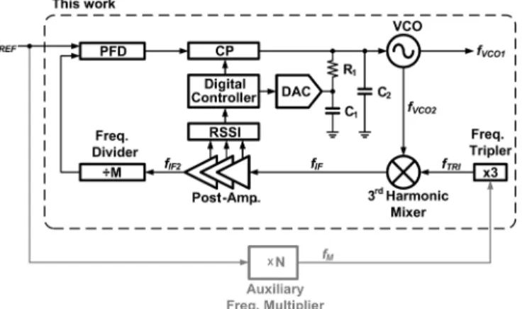
Fig. 1. FT-PLL architecture.
can be easily scaled down by digital divider. Besides, a re-ceived signal strength indicator (RSSI) is used for automatic frequency sweeping to overcome PVT variations and extend locking range.
This paper is organized as follows. Section II describes the proposed FT-PLL architecture and operation principle. The system behavior is discussed in Section III. Section IV describes the detailed circuit schematic. Experimental results are shown in Section V, and Section VI concludes this paper.
II. ARCHITECTURE
Fig. 1 depicts the proposed FT-PLL architecture. The sub-THz output frequency is generated from an on-chip LC oscillator. To down convert for phase comparison, an auxiliary frequency multiplier generates
, whose output frequency is then tripled by an on chip frequency tripler to drive a 3rd harmonic mixer. Through harmonic mixing with , is translated to a much lower frequency band [8], and then enlarged by a post amplifier to drive a digital frequency divider (1/M). When the loop is locked, we have
(1) (2) (3) It can be seen that the frequency tripler incorporating with 3rd harmonic mixer performs the same function as a 1/9 prescaler, and can be adjusted by programming the divide ratio M or the frequency multiplication factor N. To alleviate bandwidth requirement of frequency tripler, is fixed in this design. It also facilitates the optimization of frequency tripler and har-monic mixer. Besides, the bandwidth of post amplifier is de-signed to cover the frequency tuning range of . It
en-1549-8328 © 2014 IEEE. Personal use is permitted, but republication/redistribution requires IEEE permission. See http://www.ieee.org/publications_standards/publications/rights/index.html for more information.
Fig. 2. PLL with RSSI assisted frequency tracking scheme.
larges the signal swing of to logic level for a proper opera-tion of digital divider.
Using a mixer for frequency down conversion, the alternative solution of is at . To avoid this ambiguity, the oscillator free running frequency is preset to its highest fre-quency at the onset of frefre-quency switching, which is higher than
to guarantee a single mode operation.
The procedure for phase and frequency locking is described as follows. When the channel switching command is issued, the VCO is preset to its highest frequency controlled by a 3 bits re-sistor ladder DAC, and the PLL is opened loop by disabling the charge pump current. Meanwhile, the received signal strength indicator (RSSI) continues monitoring the power level at . Fig. 2 illustrates the frequency acquisition scheme incorporating RSSI. The harmonic mixer output is fed into a post voltage am-plifier, and the RSSI is composed of a rectifier followed by an envelope detector and a comparator. The comparator output is stored in a digital controller to adjust the resistor ladder DAC. Once the DAC output is renewed, the envelope detector will be reset to track the new signal amplitude at . Meanwhile, the VCO frequency is adjusted by charging the loop filter capacitor through DAC. By the low-pass nature of the post voltage amplifier, for , a higher leads to a smaller received signal amplitude. According to RSSI, the dig-ital controller then updates the DAC contents in a descending way to reduce , pulling in the frequency gradually to ap-proach . As the falls into the bandwidth of post am-plifier, its signal amplitude would become sufficiently larger to toggle the post frequency divider properly, as is illustrated in Fig. 2.
Moderated by the RSSI and level detector, this pull-in process will be finished when the signal amplitude at exceeds the threshold level to drive the succeeding frequency divider. In this design, the input sensitivity of the post divider is around 150 mV, thus the threshold voltage of comparator is set to 180 mV to tolerate 20% PVT variation. The 3 bits DAC provides voltage tuning range of 0.9 V and corresponding frequency tuning range of 3 GHz. As the DAC is updated at 4 MHz, the frequency sweeping time is less than 2 . After the pull-in process mon-itored by RSSI, the digital controller then resumes the close loop operation by enabling the charge pump current, and keeps phase tracking . The proposed frequency sweeping scheme brings into its target frequency automatically, al-leviating bandwidth requirement of the feedback path of PLL without sacrificing its locking range.
Fig. 3. (a) Frequency-translation PLL behavioral model (b) noise model.
III. BEHAVIORALMODEL
To investigate behavior and phase noise performance of the proposed FT-PLL, its linear model is illustrated in Fig. 3(a). Here represents the gain of phase frequency detector (PFD)
and charge pump (CP), denotes VCO gain, and
respectively represent the transfer function of loop filter and post amplifier. The linear model of 3rd harmonic mixer and frequency tripler is illustrated in the dashed box, which provides phase offset of in the feedback path. The phase transfer function of to can be derived as
(4)
where . When the PLL is operating
in phase tracking mode, falls within the post amplifier’s 3 dB bandwidth, and the phase shift caused by is negligible . Thus the system transfer function can be simplified as
(5)
which is the same as that of a conventional PLL with fre-quency multiplication factor of . Fig. 3(b) illustrates the phase noise contribution from individual building blocks,
where, , , and respectively
represent the noise source from reference input, loop filter, VCO, and frequency divider in a typical charge-pump based PLL. Their impacts on the VCO phase noise can be respectively represented as
where represents the reference phase noise transfer func-tion (low pass filtering) of the auxiliary PLL, whose DC gain equals to (frequency multiplying factor), and
denotes other noise sources coming from the auxiliary PLL. Defining the excess noise source in the frequency-translation
PLL (FT-PLL) as , where
(11) We have
(12) Combing (6) and (12), it reveals that the reference phase noise transfer function can be described as
(13) whose DC gain equals to . The 1st term corre-sponding to is noise shaped by the cascaded loop filter , which facilitates optimization compared to a single loop architecture [9]. Meanwhile, the other terms in are translated to VCO output as in-band noise without amplifica-tion. According to (7)–(9), the noise contribution from
and in the main loop is reduced from to
in contrast to a single loop PLL. Additionally, in-band noise from VCO is suppressed by increasing the loop gain (feedback factor increases by compared to single loop PLL). It provides some design margin to accommodate noise degradation caused by .
To sum up, the FT-PLL output phase noise , can be expressed as
(14) Provided that the reference noise floor is 150 dBc/Hz at
1 MHz offset, and , the loop bandwidth is
chosen where the out-of-band noise and the loop noise con-tribute equally to the output jitter, the simulated in band phase noise is about 89 dBc/Hz.
IV. BUILDINGBLOCKS
Design considerations of the individual building blocks are described as follows.
A. Voltage Controlled Oscillator
As approaches devices’ , the parasitic resistance introduced by the LC tank and its succeeding buffer stages becomes a critical issue to maintain stable oscillation. Mean-while, the parasitic capacitance severely limits the oscillation frequency of VCO. To overcome the design challenges, a transformer-based VCO is adopted.
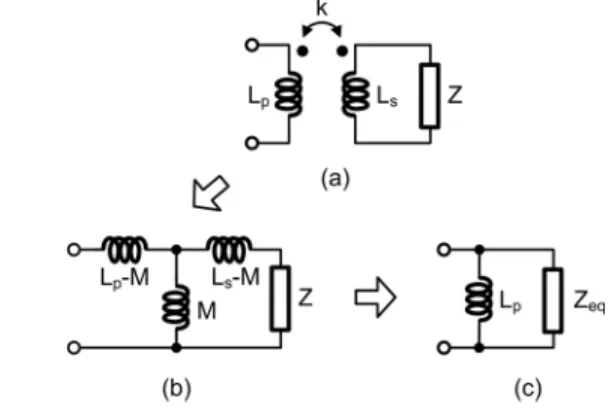
To demonstrate the advantage of capacitive degeneration through magnetic coupling, Fig. 4(a) exemplifies a two-coil model for simplicity [10]. For a two-coil transformer with primary coil inductance of , secondary coil inductance of , mutual inductance of M, and coupling factor of , its equivalent T-model can be depicted as shown in Fig. 4(b). When the secondary port is loaded with impedance , the equivalent impedance seen from the primary port and paralleled with , as shown in Fig. 4(c), becomes
(15) By choosing , the loading effect associated with the secondary port can be reduced accordingly.
Fig. 5 illustrates the detail circuit schematic. The VCO core is composed of negative impedance converter and the primary coil of the transformer, while the varactors, buffer stage, and harmonic mixer are coupled to the resonator through an outer coil and inner coil respectively. As
(16) it also degenerates the tuning sensitivity of the varactor to main-tain a high frequency oscillation. Meanwhile, the transformer coupling also provides voltage gain between the primary and secondary ports, where
(17) It provides the advantage to generate a higher voltage swing at the input of 3rd harmonic mixer. The detail layout of the triple-coil transformer and its parameters are also summarized in Fig. 5.
The transformer is laid out as micro strip lines using top metal, providing inductance of about 27.5 pH and self-resonant frequency of about 372 GHz. The coupling coefficients from the primary coil to the secondary and the third coil are about 0.103
Fig. 5. VCO schematic.
and 0.335 respectively. By impedance transformation, the par-asitic capacitance and resistance seen at the resonator are about 13 fF and 243 as referred to the primary coil. For a varactor tuning range from 6.7 fF to 16.6 fF, the measured tuning range of the VCO is from 156.4 GHz to 159.2 GHz.
B. Frequency Tripler
Fig. 6 illustrates the circuit schematic of frequency tripler. The frequency tripler [11] is configured as a synchronous lock oscillator composing of , , and LC tank, whose output frequency is tuned at . The excitation signal provided by the auxiliary frequency multiplier is injected differentially at and to generate the third harmonic tone of , which is provided to synchronize the injection locked oscillator. Since both the and frequencies are fixed, it facilitates the optimization of the tripler design with maximum power gain by properly choosing the resonant frequency of the tank. As the locking range of the frequency tripler can be de-scribed as [12]
(18) where and represent the center frequency and quality factor of the LC tank, represents the third harmonic drain current of and , and represents the DC current of the injection locked oscillator. The 3rd harmonic of the transconductance of and can be maximized to enhance the injection efficiency by properly choosing their conduction angle [13]. The strength of the third harmonic component under different conduction angle can be evaluated by normal-izing its amplitude to that of the overall drain current , where
(19)
As shown in Fig. 7, the frequency tripler has the highest injec-tion efficiency at the conducinjec-tion angle of about 80 . Under this
Fig. 6. Frequency tripler schematic.
Fig. 7. Injection efficiency of frequency tripler under different conduction angle.
Fig. 8. 3rd harmonic mixer schematic.
circumstance, and are biased at sub-threshold region, which may cause the oscillator fail to start oscillation due to limited DC current. To overcome this issue, a conduction angle of about 240 is chosen in this design for a higher injection ef-ficiency while meeting the oscillation criterion.
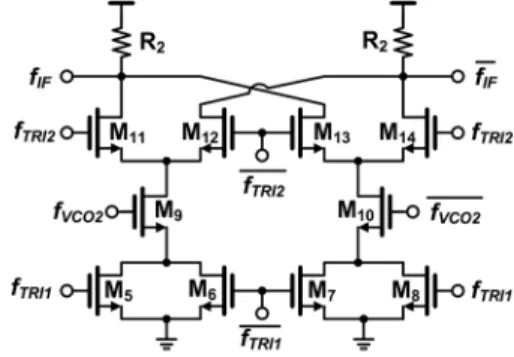
C. 3rd Harmonic Mixer
Fig. 8 illustrates the circuit schematic of 3rd harmonic mixer. It is composed of frequency doubler , a single transistor mixer , and a double-balanced
Gilbert switches in cascode to reduce power
consumption. is injected differentially to the transistor and , and the VCO output is applied
to as .
Let
(20) and
of and , and denotes the DC voltage.
From (23), it can be seen that the odd order harmonics of are cancelled out at the source of and , while its even order harmonics remain. To maximize the second order harmonic tone of the frequency doubler, to are biased at subthreshold region to perform as ideal switches and boost the harmonic tones.
As the overdrive voltage of and are modulated by the second order harmonic of and , they perform as single transistor mixers through the nonlinearity of MOSFET I-V characteristic. Their output currents become
(24) where
(25) The other high frequency terms due to leakage
and harmonic tones are low pass filtered at the input of Gilbert switches. Thus the drain currents of and are translated
to and flow through the commutating stages
driven by again.
The resulting down converted signal is at
, and the unwanted spurs at and
are also filtered out by the RC low pass filter. If is modeled as ideal switches, the conversion gain
of the third harmonic mixer can be derived as
(26) If
(27) Combing (26) and (27), we have
(28) According to (28), can be enhanced by increasing and decreasing the overdrive voltage of and ,
Fig. 9. Post-amplifier schematic.
Fig. 10. (a) Offset-cancellation amplifier (b) gain cell.
which leads to a higher nonlinearity of the single transistor mixer. With on chip VCO amplitude of about 100 mV and tripler output amplitude of about 250 mV, the simulated con-version gain of the third harmonic mixer is about 28 dB.
D. Post-Amplifier and RSSI
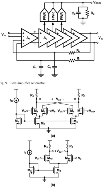
Fig. 9 shows the post-amplifier architecture. It is composed of an offset cancellation input stage followed by five identical gain cells and an low pass filter for offset extraction. The offset cancellation stage and the gain cells are basically common source amplifiers, as are shown in Fig. 10(a) and Fig. 10(b) respectively. The post amplifier provides a DC gain of 60 dB, and 3 dB bandwidth of about
1 GHz . If falls within the 3 dB
band-width of the post amplifier, it would be enlarged to be higher than 324 mVpp to drive the divider for phase and frequency comparison.
The post amplifier output is connected to a full wave rectifier to perform as received signal strength indicator (RSSI). Fig. 11 shows the detailed circuit schematic. The output voltage is
con-Fig. 11. Full wave rectifier for RSSI.
Fig. 12. Simulated frequency dependent output voltage characteristic of RSSI.
Fig. 13. Charge pump schematic.
verted to current form by and , and rectified through
current mirrors and . The RSSI
mani-fests pseudo linear frequency dependent transfer characteristic, as is shown in Fig. 12. It fully covers the tuning range of the VCO to assist frequency pull-in process.
At the onset of frequency lock-in process, the VCO is preset to its highest frequency, leading to a smaller output at the RSSI. The VCO frequency is then pulled down gradually by a resistor-ladder DAC, which is controlled by the RSSI. As RSSI exceeds the threshold level, the post amplifier output is large enough to make the succeeding dividers function properly. The PLL will resume its close loop operation for frequency locked and phase tracking.
E. Charge Pump
Fig. 13 shows the charge pump circuit. To alleviate reference spurs induced by current mismatch, wide swing cascode current
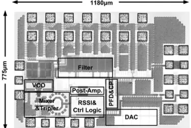
Fig. 14. Chip photograph.
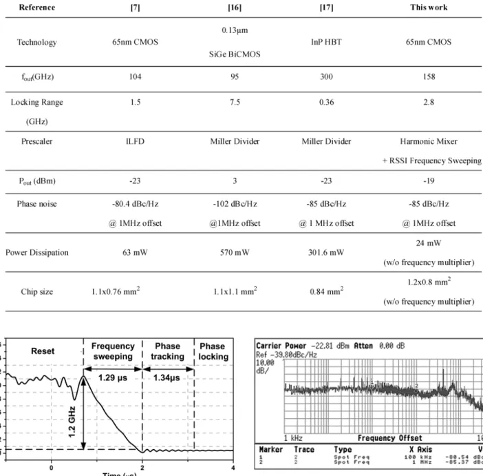
Fig. 15. Measured PLL output spectrum at 157.82 GHz with .
mirrors are adopted to copy the up and down currents. Here
and are replicas of and .
V. EXPERIMEANTALRESULTS
A 160 GHz frequency-translation PLL has been fabricated using TSMC 65 nm CMOS process, and is powered under a 1.2 V supply. The total power dissipation is about 24 mW and
the chip size is about , excluding the
fre-quency multiplier. The chip photo is shown in Fig. 14. The chip performance is measured using probe station. The VCO output frequency is down converted by an external harmonic mixer (OML M05HWD) and measured by frequency spectrum ana-lyzer (Agilent E4448A). With a reference frequency of
130 MHz, at 17.42 GHz , and , the
mea-sured output spectrum is shown in Fig. 15. By taking the inser-tion loss ( 55 dB) of external mixer and cable into account, the output power of VCO is 19 dBm. The measured locking time using signal source analyzer (Agilent E5052A) is less than 3 by the proposed frequency acquisition scheme, as is shown in Fig. 16.
Due to the limitation of in house instruments, the VCO phase noise performance is indirectly measured at the post amplifier
Fig. 16. Measured PLL settling behavior at (For hopping from 158.92 GHz to 157.82 GHz, changes from 2.14 GHz to 1.04 GHz).
output . Fig. 17 shows the measured phase noise perfor-mance. According to the previous discussions in Section III, the phase noise performance at amplifier output can be modeled as
(29) By taking the noise contribution of into account, the VCO phase noise is expected to be better than 85 dBc/Hz at 1 MHz offset.
Table I summaries the performance benchmark. It can be seen that the resonator based divider (ILFD/Miller) are facing severe design challenges as operating frequency beyond 100 GHz. Taking the estimated power of auxiliary PLL into account [15],
Fig. 17. Measured phase noise performance at .
the proposed FT-PLL architecture still manifests superiority in low power consumption by circumventing 1/9 millimeter wave prescaler. Additionally, by RSSI assisted automatic frequency sweeping, it can achieve reliable operation without external tuning.
VI. CONCLUSION
This paper proposes a novel frequency-translation PLL for sub-THz systems. High frequency prescaler in the PLL is re-placed by a 3rd harmonic mixer for frequency down conver-sion. In contrast to conventional PLL with cascaded ILFDs as prescaler, it is free of frequency misalignment problems with the aid of RSSI for automatic frequency sweeping. Finally, a 160 GHz fundamental mode PLL with agile locking speed is demonstrated using TSMC 65 nm CMOS process.
REFERENCES
[1] H. Sherry et al., “A 1 kpixel CMOS camera chip for 25 fps real-time ter-ahertz imaging applications,” in Proc. ISSCC Dig. Tech. Papers, Feb. 2012, pp. 252–254.
[2] K. Sengupta and A. Hajimiri, “A 0.28 THz 4 4 power-generating and beam-steering array,” in Proc. ISSCC Dig. Tech. Papers, Feb. 2012, pp. 256–258.
[3] D. Huang et al., “324 GHz CMOS frequency generator using linear su-perposition technique,” in Proc. ISSCC Dig. Tech. Papers, Feb. 2008, pp. 476–629.
[4] E. Seok et al., “A 410 GHz CMOS push-push oscillator with an on-chip patch antenna,” in Proc. ISSCC Dig. Tech. Papers, Feb. 2008, pp. 472–629.
[5] J. Lee, “A 75-GHz PLL in 90-nm CMOS technology,” in Proc. ISSCC
Dig. Tech. Papers, Feb. 2007, pp. 432–613.
[6] K.-H. Tsai and S.-I. Liu, “A 43.7 mW 96 GHz PLL in 65 nm CMOS,” in Proc. ISSCC Dig. Tech. Papers, Feb. 2009, pp. 276–277. [7] K.-H. Tsai and S.-I. Liu, “A 104-GHz phase-locked loop using a VCO
at second pole frequency,” IEEE Trans. Very Large Scale Integr. Syst., vol. 20, no. 1, pp. 80–88, Jan. 2012.
[8] J.-M. Hsu, “A 0.18-mm CMOS offset-PLL upconversion modulation loop IC for DCS1800 transmitter,” IEEE J. Solid-State Circuits, vol. 38, no. 4, pp. 603–613, Apr. 2003.
[9] B. Razavi, “The role of PLLs in future wireline transmitters,” IEEE
Trans. Circuits Syst. I, Reg. Papers, vol. 56, no. 8, pp. 1786–1793, Aug.
2009.
[10] L. L. K. Leung, K. W. C. Chui, and H. C. Luong, “A 1 V dual-band VCO using an integrated variable inductor,” in ASSCC, Nov. 2005, pp. 273–276.
[11] M.-C. Chen and C.-Y. Wu, “Design and analysis of CMOS subhar-monic injection-locked frequency triplers,” IEEE Trans. Microw.
Theory Tech., vol. 56, no. 8, pp. 1869–1878, Aug. 2008.
[12] B. Razavi, “A study of injection locking and pulling in oscillator,”
IEEE J. Solid-State Circuits, vol. 39, pp. 1415–1424, Sep. 2004.
[13] Z. Chen and P. Heydari, “An 85–95.2 GHz transformer-based injec-tion-locked frequencyTripIer in 65 nm,” in Proc. IEEE Microw. Symp.
Digest, May 2010, pp. 776–779.
[14] M.-F. Huang et al., “Analysis and implementation of a CMOS even harmonic mixer with current reuse for heterodyne/direct conversion receivers,” IEEE Trans. Circuits Syst., vol. 52, no. 9, pp. 1741–1750, Sep. 2005.
[15] A. W. L. Ng et al., “A 1-V 24-GHz 17.5-mW phase-locked loop in a 0.18-m CMOS process,” IEEE J. Solid-State Circuits, vol. 41, no. 6, pp. 1236–1244, June 2006.
[16] S. Kang, J.-C. Chien, and A. M. Niknejad, “A 100 GHz phase-locked loop in 0.13 SiGe BiCMOS process,” in Proc. IEEE Radio Freq.
Integrated Circuits Symp., Jun. 2011, pp. 1–4.
[17] M. Seo1 et al., “A 300 GHz PLL in an InP HBT technology,” in Proc.
IEEE Int. Microw. Symp. Dig., Jun. 2011, pp. 1–4.
Wei-Zen Chen received the B.S., M.S., and Ph.D.
degrees in electronics engineering from National Chiao-Tung University, Hsin-Chu, Taiwan, in 1992, 1994, and 1999, respectively.
He was with ITRI/ERSO in 1999 involved in the development of CMOS RF ICs for cellular and wire-less LAN applications. From 1999–2002, he was an Assistant Professor at the Department of Electrical Engineering, National Central University, Chung-Li, Taiwan. Since 2002, he joined the Department of Electronics Engineering, National Chiao-Tung Uni-versity, where he is now a full Professor. His research focuses on mixed-signal integrated circuit for wireless and wireline communication systems, with special emphasis on Serdes, high speed interface, optical communication, wireless PAN, LAN, and body area network applications.
Dr. Chen was the deputy executive director of National SoC (NSoC) Program in Taiwan from 2009–2011, and is the principal investigator of National Project on Intelligent Electronics (NPIE) in Taiwan since 2011. He also served as IEEE
Solid-State Circuit Society Taipei Chapter chairman from 2008–2012. He was the technical program vice chair of 2008 VLSI/CAD design symposium, tech-nical program chair of 2012 symposium on engineering, medical, and biology applications (SEMBA), and the guest editor of International Journal of Elec-trical Engineering (IJEE). He is a member of Phi-Tau-Phi honorary scholar so-ciety, and also served as technical program committee member of IEEE Custom Integrated Circuits Conference (CICC), IEEE Asian Solid-State Circuit Confer-ence (A-SSCC), IEEE RFIT, and IEEE ASICON.
Tai-You Lu was born in Taipei, Taiwan, in 1980.
He received the B.S. degree in electrical engineering from National Cheng-Kung University, Tainan, Taiwan, in 2003, and the Ph.D. degree in electronics engineering from National Chiao Tung University, Hsinchu, Taiwan, in 2011.
He has been with MediaTek Inc., Taiwan, since 2011, where he is working on mixed-signal integrated circuit design for communication systems.
Dr. Lu is a member of Phi Tau Phi honorary scholar society.
Yan-Ting Wang was born in Chiayi, Taiwan, in
1986. She received the B.S. degree in electrical control engineering from National Chiao-Tung University, Taiwan, in 2009, and the M.S. degree in the Institute of Electronics, National Chiao-Tung University, Hsinchu, Taiwan, in 2012.
Jhong-Ting Jian was born in Taipei, Taiwan,
on April 8, 1987. He received the B.S. degree in electrical engineering from National Sun Yat-Sen University, Kaohsiung, Taiwan, in 2009 and M.S. degree in electronic engineering from National Chiao-Tung University, Hsinchu, Taiwan, in 2012.
He subsequently joined the LTPS department of Sitronix Technology Corporation, Taipei, Taiwan. Since then he has been engaged in the research and development of CMOS mixed-signal circuit for high resolution display driver IC.
Yi-Hung Yang was born in Taipei, Taiwan, on
June 19, 1987.He received the B.S. degree in the Department of Electrical Engineering from National Sun Yat-Sen University, Taiwan, and the M.S. degree in the Institute of Electronics from National Chiao-Tung University, Taiwan, in 2009 and 2012, respectively.
Kai-Ting Chang was born in Taichung, Taiwan, in
1988. She received the B.S. degree in electrical en-gineering from National Central University, Taiwan, in 2011. She is currently working toward the M.S. degree at National Chiao-Tung University, Hsinchu, Taiwan.