國
立
交
通
大
學
電機學院 電子與光電學程
碩
士
論
文
積體電路產品之元件充電模式
靜電放電測試與研究
Investigation on Board-Level and Chip-Level
Charged-Device-Model ESD Issues in IC Products
研 究 生:黃志國
指導教授:柯明道 教授
積體電路產品之元件充電模式
靜電放電測試與研究
Investigation on Board-Level and Chip-Level
Charged-Device-Model ESD Issues in IC Products
研 究 生:黃志國 Student:Chih-Kuo Huang 指導教授:柯明道 Advisor:Ming-Dou Ker
國 立 交 通 大 學
電機學院 電子與光電學程
碩 士 論 文 A ThesisSubmitted to College of Electrical and Computer Engineering National Chiao Tung University
in partial Fulfillment of the Requirements for the Degree of
Master of Science in
Electronics and Electro-Optical Engineering November 2009
積體電路產品之元件充電模式
靜電放電測試與研究
學生: 黃 志 國 指導教授: 柯 明 道 教授
國立交通大學
電機學院 電子與光電學程碩士班
摘要
隨著近年來半導體積體電路製程的持續演進,元件尺寸越做越小,已朝向奈米範 疇發展,並且由於積體電路運算速度的發展需求,互補式金氧半導體(CMOS)製程技 術持續進展,並降低電晶體的閘極氧化層厚度,以提升電路工作頻率;但對靜電放電 (Electrostatic Discharge, ESD)而言,較薄的閘極氧化層厚度,意味著電晶體閘極更容 易遭受靜電放電轟擊而毀損。在先進互補式金氧半(CMOS)製程中,這種電晶體閘極 毀損的情況,在晶片層級元件充電模式(Chip-Level Charged-Device-Model, CDM)靜電 放電測試時極為明顯。然而在電子產品應用中,當晶片黏貼至電路板上時,若電路板 本身因為摩擦或感應而累積電荷,電路板上累積的電荷,會經由電荷重新分配的過程 傳遞至晶片中,並瞬間產生非常大的電流流入晶片,造成晶片損壞,此為電路板層級 元件充電模式(Board-Level CDM)靜電放電的成因。 本篇論文的第一部份在探討電路板層級(Board-Level)及晶片層級元件充電模式 (Chip-Level CDM)靜電放電在積體電路產品上的行為特性研究與所造成的威脅,且針 對實際實驗案例,以故障分析(Failure Analysis)的手法,進行對遭受晶片層級元件充 電模式靜電放電測試損害之元件作故障定位(Fault Isolation),並找出元件充電模式靜 電放電所造成之故障機制(Failure Mechanism)比較及探討。本篇論文的第二部份是以實驗模擬的方式,對數個以互補式金氧半製程製作的測 試元件與測試電路進行電路板層級與晶片層級元件充電模式靜電放電測試,首先由於 電路板層級元件充電模式靜電放電的電流峰值與電子模組中的電路板尺寸有密切的 關係,故針對不同電路板尺寸所產生的電路板層級元件充電模式靜電放電波形進行量 測,實驗結果顯示較大的電路板尺寸或將電路板充電至較高電壓,將導致較大的電路 板層級元件充電模式靜電放電電流峰值;其次針對測試元件與測試電路進行電路板層 級與晶片層級元件充電模式靜電放電測試,測試結果發現電路板層級元件充電模式靜 電放電耐受度較低,且證實電路板層級元件充電模式對積體電路產品所造成的損害, 遠比晶片層級元件充電模式來的嚴重。 本論文透過實驗的結果,成功證明電路板層級元件充電模式靜電放電在積體電路 產品所造成的損害,遠比晶片層級元件充電模式來的嚴重,而且常容易被誤認為過度 電性應力(Electrical Over Stress, EOS),由於目前對電路板層級的靜電放電測試尚未有 明確規範,經由本論文實驗步驟的建立,可供日後規範建立的參考。
Investigation on Board-Level and Chip-Level
Charged-Device-Model ESD Issues in IC Products
Student: Chih-Kuo Huang Advisor: Prof. Ming-Dou Ker
Degree Program of Electrical and Computer Engineering National Chiao Tung University
ABSTRACT
With the continuous evolution of semiconductor integrated circuit (IC)
process, the device dimension growing narrow down and developing into
nanoscale. Moreover, the transistors have been fabricated with thinner gate
oxides to achieve higher speed or operation frequency due to the operation
speed requirement of integrated circuits (ICs) in advanced process of
complementary metal-oxide semiconductor (CMOS). In electrostatic
discharge (ESD) events, the transistors are more easily damaged during ESD
stress if they are fabricated with thinner gate oxides. The situation of gate
oxide damage of transistors is a typical and familiar failure mechanism during
chip-level charged-device-model (CDM) ESD test, especially in CMOS
process. But in the applications of microelectronic system, IC chips must to
be attached to the printed circuit board (PCB). The static charges will be
stored in the PCB due to induction or rub and then deliver the charges to the
IC chips through redistribution process during the attachment of IC chips to
PCB. The instantaneous current flows into the IC chips is huge and will result
In the first part of this thesis, the focus is the investigation of
characteristics and threats on board-level and chip-level CDM ESD in IC
products. Furthermore, from the experimental results, the technique of failure
analysis (FA) with fault isolation is applied to summarize the comparison of
CDM failure mechanism caused by ESD event during CDM ESD test.
The second part presents an experiment of ESD test between board-level
and chip-level CDM on several samples fabricated with CMOS process. At
first, the board-level CDM ESD current waveforms under different sizes of
printed circuit boards (PCBs) and different charged voltage are measured. The
experiment result has shown that the discharging current strongly depends on
the PCB size and the charged voltage. Moreover, chip-level and board-level
CDM ESD levels of several test devices and test circuits have been
characterized and compared. Test results have shown that the board-level
CDM ESD level of the test circuit is lower than the chip-level CDM ESD
level, which demonstrates that the board-level CDM ESD event is more
critical than the chip-level CDM ESD event. In addition, failure analysis
reveals that the failure on the test circuit under the board-level CDM ESD test
is much severer than that under the chip-level CDM ESD test.
Based on the experiment results in this thesis, it is successfully proved that
the failures caused by board-level CDM ESD event are more server than
chip-level CDM ESD event and are easily mistaken for electrical over stress
(EOS) related failures. Since the standard for the board-level CDM ESD test
誌 謝
ACKNOWLEDGMENT
首先要感謝的是我的指導教授柯明道博士,這六年來的耐心教導和鼓勵,無論在 論文上的寫作、研究的心得與方法、以及精神上的鼓舞,都給予我莫大的激勵與支持, 才能順利完成本論文的寫作,於此誠摯致上無限的謝意與感激;指導教授已多次指正 學生論文之失誤或不完整之處,若本論文中仍有小錯誤之處,皆由學生負責承擔。 在論文研究歷程中,承蒙閎康科技總經理謝詠芬博士,在整個實驗計畫上所提供 的協助與指導,並提供寶貴實務意見,在學生遇到瓶頸及困難時,總是不厭其煩且耐 心的教導,師恩浩瀚,永銘記在心。 另感謝同是交通大學奈米電子與晶片系統實驗室的蕭淵文、顏承正、王暢資、林 群祐、陳穩義、黃俊、邱柏硯等學長和同學學弟們,在求學期間給予的協助與指導, 不管是在專業上還是生活上所遇到的問題,都能適切誠懇地幫助關心我度過難關,使 研究所生涯更豐碩。 最後要由衷感謝敬愛的父親黃慶祥先生、母親林秀玉女士及我內人譚海倩女士及 寶貝弘勳、雯暄,他們在此段期間給予我全力的支持、協助與體諒,使我能全心全意 完成論文。另感謝我的親友們對我的關懷與協助。你們是背後支撐我的最大力量,願 大家平安喜樂。 黃 志 國 謹誌於竹塹交大 九十八年 冬CONTENTS
ABSTRACT (CHINESE)
i
ABSTRACT (ENGLISH)
iii
ACKNOWLEDGMENT
v
CONTENTS
vi
TABLE CAPTIONS
viii
FIGURE CAPTIONS
ix
CHAPTER 1 INTRODUCTION
1
1.1 Background of ESD and Electrical Over Stress (EOS) 1
1.2 ESD Testing for HBM, MM, and CDM 3
1.3 Diagnosis of Possible Damage Sites on ESD
Protection Circuit 11
1.4 Board-Level Charged-Device-Model (CDM) ESD
Issue 17
1.5 Organization of This Thesis 19
CHAPTER 2 FAILURE ANALYSIS OF CDM ESD
EVENT
20
2.1 Chip-Level CDM ESD Event in IC Products 20
2.2 Fault Isolation Techniques on CDM ESD Failure 22
2.3 Case Study on Chip-Level CDM ESD Damage 25
3.2 Experimental Results and Discussion 40 3.2.1 Board-Level CDM ESD Current Waveforms
in Different PCBs 40
3.2.2 Test with ESD Testkey of Grounded Gate
NMOS (GGNMOS) 43
3.2.3 Test With Dummy Receiver NMOS
(RX_NMOS) 46 3.2.4 Test With 2.5-GHz High-Speed Receiver
Interface Circuit 51
3.3 Summary 55
CHAPTER 4 CONCLUSIONS AND FUTURE
WORKS
56
4.1 Main Results of This Thesis 56
4.2 Future Works 57
REFERENCES
58
VITA 61
PUBLICATION LIST
61
TABLE CAPTIONS
CHAPTER 1
Table 1.1 Comparison of ESD and EOS. 3
Table 1.2 The summary of the ESD zap numbers including the polarity and the minimum zap interval according to the
standards, MIL, ESDA, JEDEC, and AEC. 11
Table 1.3 Summary of ESD failure location with respect to failure
mechanism. 17
CHAPTER 2
Table 2.1 Characteristics of four fault isolation tools. 23
CHAPTER 3
Table 3.1 Characteristics of three different kinds of PCBs. 39
Table 3.2 Chip-level CDM and board-level CDM ESD robustness
of GGNMOS. 45
Table 3.3 Chip-level CDM and board-level CDM ESD robustness
of RX_NMOS. 49
Table 3.4 Chip-level CDM ESD robustness of 2.5-GHz high-speed
receiver interface circuit. 52
Table 3.5 Board-level CDM ESD robustness of 2.5-GHz
high-speed receiver interface circuit. 52
FIGURE CAPTIONS
CHAPTER 1
Fig. 1.1 Comparison of pulse duration on ESD and EOS. 2
Fig. 1.2 Equivalent circuits of (a) HBM, and (b) MM, ESD tests. 4
Fig. 1.3 Equivalent circuits of CDM ESD test. 5
Fig.1.4 Four ESD test pin combinations for IC products: (a)
positive-to-VDD mode (PD Mode), (b) negative-to-VDD mode (ND Mode), (c) positive-to-VSS mode (PS Mode),
and (d) negative-to-VSS mode (NS Mode). 6
Fig. 1.5 Pin combinations in VDD-to-VSS ESD test: (a) positive
mode, and (b) negative mode. 7
Fig. 1.6 Pin combinations in pin-to-pin ESD test: (a) positive mode,
and (b) negative mode. 7
Fig. 1.7 Architecture of socketed CDM (SDM) ESD test. 8
Fig. 1.8 Non-socketed CDM test equipment (Oyrx CDM Orion). 9
Fig. 1.9 Discharge current waveforms of three ESD stress models (HBM, MM, and CDM).
10
Fig. 1.10 Typical double-diode whole-chip ESD protection scheme
for ICs. 12
Fig. 1.11 ESD current path in the typical double-diode whole-chip
ESD protection scheme under PS-mode ESD stress. 13
Fig. 1.12 ESD current path in the typical double-diode whole-chip
ESD protection scheme under ND-mode ESD stress. 13
Fig. 1.13 ESD current path in the typical double-diode whole-chip
ESD protection scheme under pin-to-pin ESD stress. 14
Fig. 1.14 Possible damage locations on the ESD devices under HBM, MM, and CDM ESD tests in whole-chip ESD protection
scheme for ICs. 15
ESD device by physical structure illustration (plane-view of SEM). 16
Fig. 1.16 Possible ESD damage sites/paths and mechanisms of the ESD device by physical structure illustration (cross-
sectional view of TEM). 16
CHAPTER 2
Fig. 2.1 CDM ESD event: When a certain pin is grounded, the stored charges in the IC will be quickly discharged through
the grounded pin. 20
Fig. 2.2 Typical FA procedure and flow of ESD failure analysis. 22
Fig. 2.3 HAMAMATSU Phemos-1000 Emission Microscope system. 23
Fig. 2.4 Diagram of EMMI operation principle. 24
Fig. 2.5 CDM ESD current path in an input buffer. 26
Fig. 2.6 SEM failure pictures of the failure site with gate oxide
damage in the input NMOS (MN). 26
Fig. 2.7 CDM ESD current path in (a) an output buffer circuit, and (b) the diagram of cross-sectional view. 27
Fig. 2.8 SEM failure pictures of poly gate damage on a NMOS (MN)
transistor in the internal circuit. 28
Fig. 2.9 After chip-level CDM ESD test, the failure point is located
by (a) EMMI detection, and (b) SEM inspection. 29
Fig. 2.10 After chip-level CDM ESD test, the failure point is located by (a) EMMI detection. (b) The enlarged image of its ESD
will be redistributed when the chip is attached to the PCB. 33
Fig. 2.13 When two capacitors with different voltages are shorted,
charge redistribution will occur. 33
Fig. 2.14 When a certain pin of the PCB is grounded during the module function test, huge current will flow from the PCB
through the IC to the external ground. 34
CHAPTER 3
Fig. 3.1 The non-socket CDM tester (Oyrx CDM Orion). 37
Fig. 3.2 Measurement setup of field-induced chip-level CDM ESD test. 38
Fig. 3.3 Measurement setup of field-induced board-level CDM ESD test. 38
Fig. 3.4 The LCR meter which is used for the measurement of
capacitance (Agilent 4275A). 39
Fig. 3.5 The high-frequency oscilloscope (TDS 680C). 40
Fig. 3.6 The top plate of board capacitance (CB) is connected to the
GND plate of PCB. The bottom plate of CB is the charging
plate of CDM ESD tester. 41
Fig. 3.7 Discharging current waveform of PCB_1 under +500V
charged voltage. 42
Fig. 3.8 Discharging current waveform of PCB_2 under +500V
charged voltage. 42
Fig. 3.9 Discharging current waveform of PCB_3 under +500V
charged voltage. 43
Fig. 3.10 Layout top view of ESD testkey with ESD protection
device of GGNMOS. 44
Fig. 3.11 Test circuit of ESD testkey GGNMOS for chip-level and
Fig. 3.12 Discharge current path of GGNMOS under CDM ESD test. 46
Fig. 3.13 Test circuit of RX_NMOS (dummy NMOS) for chip-level
and board-level CDM ESD tests. 47
Fig. 3.14 Discharging current waveforms of RX NMOS under (a) +200V chip-level CDM, and (b) +200V board-level CDM,
ESD tests. 48
Fig. 3.15 OBIRCH pictures show the failure sites caused by CDM ESD test were detected and located at the gate of the RX_NMOS. 50
Fig. 3.16 SEM failure pictures of gate oxide damages at RX NMOS after (a) chip-level CDM, and (b) board-level CDM, ESD tests. 50
Fig. 3.17 Test circuit of 2.5-GHz high-speed receiver interface circuit
for chip-level and board-level CDM ESD tests. 51
Fig. 3.18 SEM failure picture of the failure points on 2.5-GHz high-speed receiver front-end circuit after -1300V
chip-level CDM ESD test. 53
Fig. 3.19 SEM failure picture of the failure points on 2.5-GHz high-speed receiver front-end circuit after -900V
board-level CDM ESD test. 54
CHAPTER 1
INTRODUCTION
1.1 Background of ESD and Electrical Over Stress (EOS)
Electrical Over Stress (EOS) occurs when a voltage greater than the
maximum specified voltage is applied to any portion of an electrical device.
This excess voltage will often cause excess current to flow along some path.
If those current remains too long, heating of the device will occur, very often
this heating will result in permanent damage. On an integrated circuit device
this damage commonly manifests itself as fused metal lines, melted silicon or
other burned circuit elements and is frequently accompanied by carbonized
package epoxy deposited on the die surface after decapsulation [1]. On an
intrinsic level, EOS testing involves putting increasingly higher voltages
across a device until failure occurs. Aside from device geometry, the only
variable other than voltage and current that is needed to determine device
heating is the duration of the applied overstress (pulse). With smaller voltages,
the duration is relatively long (mS to S) but as voltages increase and pulse
widths narrow we enter the domain of ESD (Electro Static Discharge).
An ESD (Electro Static Discharge) event occurs when a static electric
charge builds up on an object (a person, tool, bench, and device) and is then
subsequently discharged to ground. Often a very large potential is built up and
the actual discharge generates a spark, the discharge event is commonly
this zap discharges through an electronic device. Semiconductor devices, such
as CMOS IC's and other computer components are particularly sensitive to
damage. A real ESD zap can have greatly variable characteristics. A pulse
will typically have a very fast rise time and short duration but voltage and
current levels will vary significantly from one event to another.
Fig. 1.1 shows the comparison of the pulse duration generated by ESD and
EOS. As it can be seen, the pulse duration (nS toμS) of ESD is shorter than
that of EOS (mS to S). The other Key difference between ESD and EOS is the
rise time of energy pulse. The typical value of rise time for ESD and EOS is 5
to 20nS and 5μS to 5mS, respectively. Both of them will damage devices by
a rapid localized heating of the semiconductor material or by rapidly creating
strong electrical fields.
Fig. 1.1 Comparison of pulse duration on ESD and EOS.
Table 1.1 also shows the comparison of pulse duration and failure
through an OM (Optical Microscope). The ESD failure signatures are most
likely observed with junction degradation, contact damage, poly melt filament
and gate oxide breaches. These damages may be only visible through delayer
and SEM inspection.
Table 1.1 Comparison of ESD and EOS.
1.2 ESD Testing for HBM, MM and CDM
An ESD pulse can be caused by several physical factors, each leading to
distinct characteristics depending on the source. These characteristic pulses
are broadly grouped into three categories: Human Body Model (HBM),
Machine Model (MM), and Charged-Device-Model (CDM). The equivalent
circuits of HBM, MM, and CDM ESD tests are shown in Fig. 1.2 and Fig. 1.3,
respectively. In the HBM standard, the circuit component to simulate the
charged human being is a 100pF capacitor in series with a 1500 ohm resistor
[2]. This network has a characteristic rise time and decay time. The
characteristic decay time is associated with the time of the network. An MM
characteristic time is associated with the electrical components used to
emulate the discharge process. In the MM standard, the circuit component is a
(a)
(b)
Fig. 1.2 Equivalent circuits of (a) HBM, and (b) MM, ESD tests.
Device
Under
Test
VESD200pF
Device
Under
Test
VESD100pF
R 1.5k ohm
R
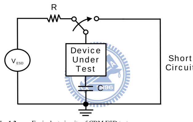
The charged-device-model (CDM) represents IC self-charging (field or
triboelectric) and then self-discharge. Currently there are two methods, one
supporting the field-induced method and the other supporting a socketed
method ESD association standard [4]. The field-induced method is more
realistic but less repeatable, whereas the socketed method is less realistic but
more repeatable.
Fig. 1.3 Equivalent circuits of CDM ESD test.
According to the standard test method of HBM and MM ESD tests, the test
pin orientations are specified with three kinds of combination as Fig. 1.4 to
Fig. 1.6 shown. The stresses may have positive or negative voltages on an I/O
pin with respect to the grounded VDD or VSS pin. For comprehensive ESD
verification, the pin-to-pin ESD stresses and VDD-to-VSS stresses had also
been specified to verify the whole-chip ESD robustness.
Device
Under
Test
VESDC
Short
Circuit
R
(a) (b)
(c) (d)
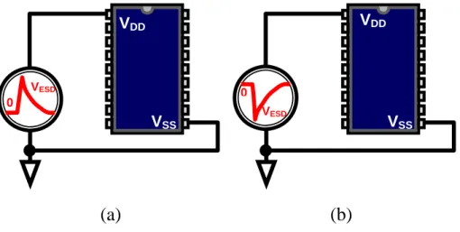
Fig. 1.4 Four ESD test pin combinations for IC products: (a) positive-to-VDD mode (PD Mode), (b) negative-to-VDD mode (ND Mode), (c) positive-to-VSS mode (PS Mode), and (d) negative-to-VSS mode (NS Mode).
I/O Pin VSS VESD 0 VSS I/O Pin VESD 0 VDD VSS I/O Pin VESD 0 0 VESD VDD I/O Pin VSS VDD VDD
(a) (b)
Fig. 1.5 Pin combinations in VDD-to-VSS ESD test: (a) positive mode, and (b) negative mode.
(a) (b)
* All power pins are floated.
Fig. 1.6 Pin combinations in pin-to-pin ESD test: (a) positive mode, and (b) negative mode.
VDD VSS I/O Pins VESD 0 VESD 0 VDD VSS I/O Pins VSS VESD 0 0 VESD VSS VDD VDD
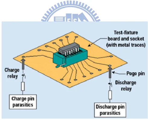
Fig. 1.7 and Fig. 1.8 show the CDM ESD test methods of socketed and
non-socketed CDM, respectively. In socketed CDM ESD test, the device
under test (DUT), socket, test fixture board, HV relays, and other parts of the
test simulator are charged and discharged during the test. The charge is
uniquely stored in a distributive network of parasitic capacitance and
inductance elements starting from the high voltage supply, the high voltage
ground relays, the pogo pins, the test fixture board, the socket, and the DUT.
Consequently, the discharge currents through the pin under test represent the
charge stored in the IC device and socketed CDM test simulator’s distributive
network.
Fig. 1.8 Non-socketed CDM test equipment (Oyrx CDM Orion).
In non-socketed CDM ESD test, two methods may be used to raise the
component potential for the subsequent CDM discharge. One is direct-
charging method and the other is filed-induced method. Since the
field-induced method is more realistic than direct-charging method, the CDM
related experiments in this thesis are tested by field-induced
method/equipment which is shown in Fig. 1.8. With the CDM ESD test, the
tested component was placed on the charging plate. Then raise the potential of
the component by energizing the field charging plate. Discharge through all
pins, including VDD and VSS pins, one at a time. The CDM discharge is
generally completed in a few nanoseconds, and peak currents of tens of
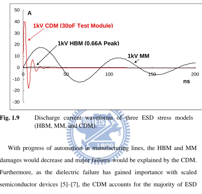
amperes have been observed. Fig. 1.9 shows the comparison of characteristic
HBM, MM, and CDM pulses, illustrating that three models impose different
requirements and as such, three models are mandatory to cover all
ESD-induced device failures. The CDM stress clearly causes much faster and
higher amplitude discharge current.
Pogo Probe
Fig. 1.9 Discharge current waveforms of three ESD stress models (HBM, MM, and CDM).
With progress of automation in manufacturing lines, the HBM and MM
damages would decrease and major failures would be explained by the CDM.
Furthermore, as the dielectric failure has gained importance with scaled
semiconductor devices [5]–[7], the CDM accounts for the majority of ESD
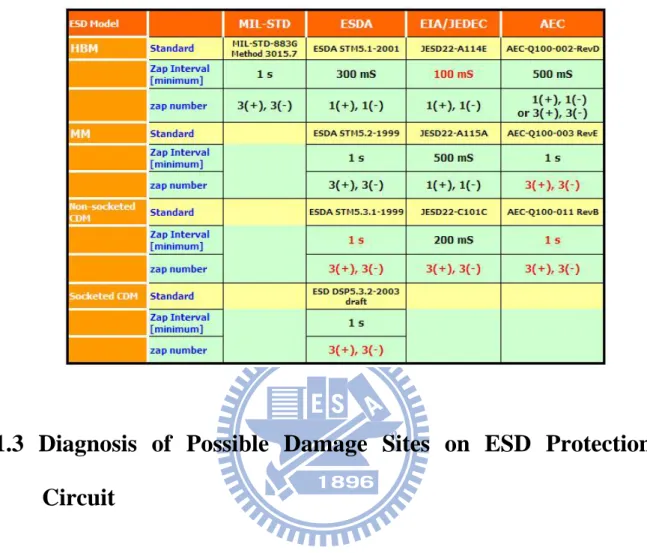
failures during chip manufacturing. Table 1.2 is the summary of the ESD zap
numbers including the polarity and the minimum zap interval according to the
standards, MIL, ESDA, JEDEC, and AEC.
-30 -20 -10 0 10 20 30 40 50 0 50 100 150 200 1kV MM 1kV HBM (0.66A Peak) 1kV CDM (30pF Test Module) A ns
Table 1.2 The summary of the ESD zap numbers including the polarity
and the minimum zap interval according to the standards, MIL, ESDA, JEDEC, and AEC.
1.3 Diagnosis of Possible Damage Sites on ESD Protection
Circuit
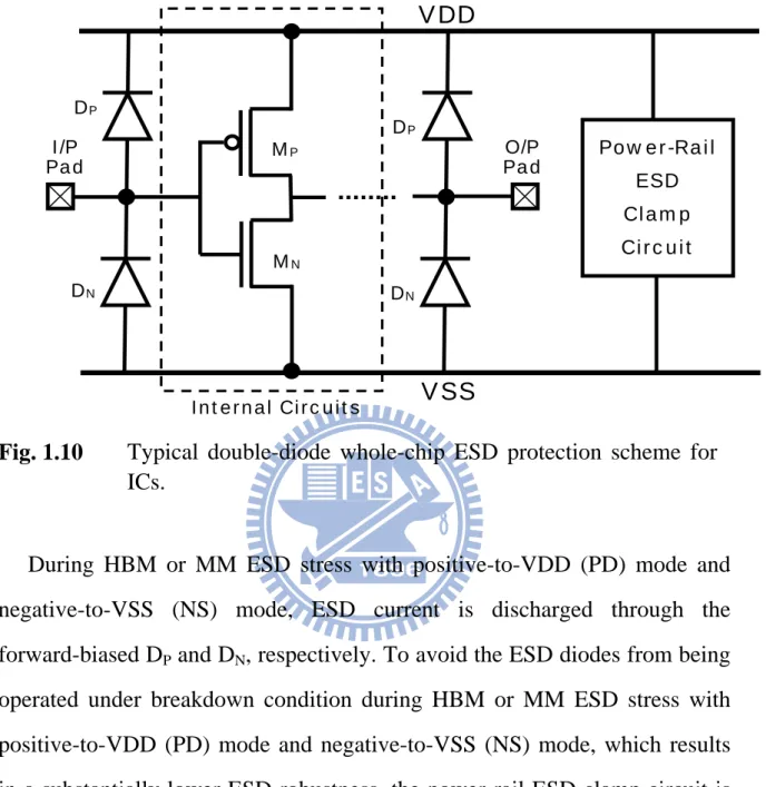
With the purpose of considering the possible ESD damage sites, the ESD
discharging current paths need to be created and constructed. Fig. 1.10 shows
the typical on-chip double-diode whole-chip ESD protection scheme in which
two ESD diodes at I/O pad are co-designed with the power-rail ESD clamp
circuit to prevent internal circuits from ESD damage [8]. In Fig. 1.10, a
P+/N-well diode (DP) and an N+/P-well diode or an N-well/P-substrate diode
(DN) are placed at input pad or output pad. When the DP and DN are under
forward-biased condition, they can provide discharge paths from I/O pad to
Fig. 1.10 Typical double-diode whole-chip ESD protection scheme for ICs.
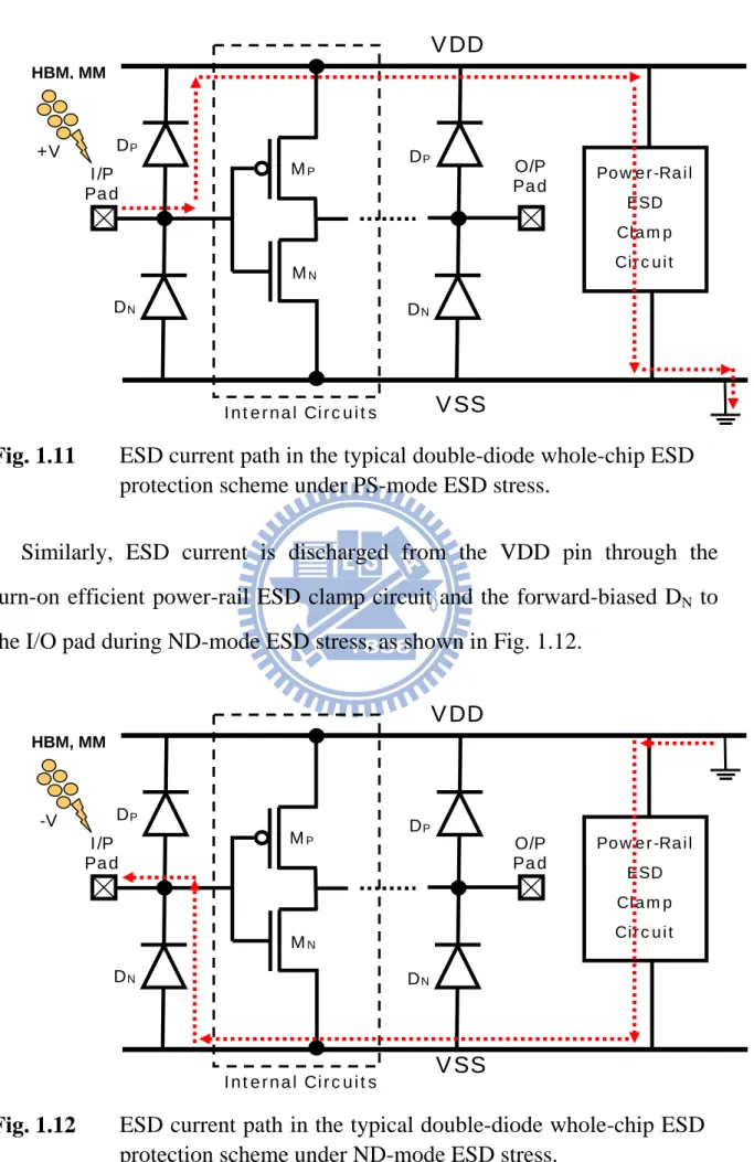
During HBM or MM ESD stress with positive-to-VDD (PD) mode and
negative-to-VSS (NS) mode, ESD current is discharged through the
forward-biased DP and DN, respectively. To avoid the ESD diodes from being
operated under breakdown condition during HBM or MM ESD stress with
positive-to-VDD (PD) mode and negative-to-VSS (NS) mode, which results
in a substantially lower ESD robustness, the power-rail ESD clamp circuit is
used between VDD and VSS to provide ESD current paths between the power
rails [9]. Thus, ESD current is discharged from the I/O pad through the
forward-biased DP to VDD, and discharged to the grounded VSS pin through
VSS
Internal Circuits DP DN I/P Pad DP DN O/PPad Power-Rail ESD
Clamp Circuit
MP
MN
Fig. 1.11 ESD current path in the typical double-diode whole-chip ESD protection scheme under PS-mode ESD stress.
Similarly, ESD current is discharged from the VDD pin through the
turn-on efficient power-rail ESD clamp circuit and the forward-biased DN to
the I/O pad during ND-mode ESD stress, as shown in Fig. 1.12.
Fig. 1.12 ESD current path in the typical double-diode whole-chip ESD protection scheme under ND-mode ESD stress.
VSS Internal Circuits DP DN I/P Pad DP DN O/P
Pad Power-Rail ESD Clamp Circuit MP MN HBM, MM -V VSS Internal Circuits DP DN I/P Pad DP DN O/P Pad Power-Rail ESD Clamp Circuit MP MN HBM, MM +V VDD VDD
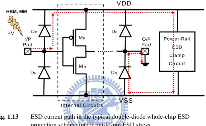
During pin-to-pin ESD stress, ESD current flows from the zapped I/O pad
through the forward-biased DP, the power-rail ESD clamp circuit, and the
forward-biased DN to the grounded I/O pad, as shown in Fig. 1.13.
Fig. 1.13 ESD current path in the typical double-diode whole-chip ESD protection scheme under pin-to-pin ESD stress.
Under VDD-to-VSS ESD test, ESD current flows through the power-rail
ESD clamp circuit between VDD and VSS. During CDM ESD test, the
charges are stored within the body of IC, ESD discharge current flows from
the body of IC through MN to the grounded I/O pad. The gate oxide of MN
would be damaged due to its thinner thickness than that of ESD protection
devices. In summary, as Fig. 1.14 shown, the possible ESD damage sites with
HBM and MM ESD stresses are most likely on the common drain of
VSS Internal Circuits DP DN I/P Pad DP DN O/P
Pad Power-Rail ESD Clamp Circuit MP MN HBM, MM +V VDD
Fig. 1.14 Possible damage locations on the ESD devices under HBM, MM, and CDM ESD tests in whole-chip ESD protection scheme for ICs.
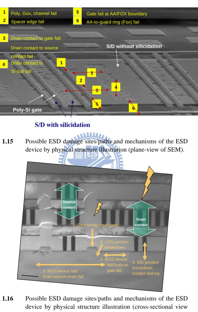
Fig. 1.15 shows the possible ESD damage sites and paths by physical
structure illustration of ESD protection device. There are typically six kinds
of damage site and mechanism as indicated in the figure. Fig. 1.16 shows the
cross-sectional view of ESD device with possible damage sites and paths by
transmission electron microscopy (TEM) inspection.
VSS VDD Internal Circuits DP DN I/P Pad DP DN O/P
Pad Power-Rail ESD Clamp Circuit MP MN HBM, MM Common drain Common drain HBM, MM CDM
S/D with silicidation
Fig. 1.15 Possible ESD damage sites/paths and mechanisms of the ESD device by physical structure illustration (plane-view of SEM).
Source contact
Drain contact
1. Gate oxide breakdown,
3. MOS device fail/Drain-to-gate fail, 2. LDD junction
breakdown,
3. MOS device fail/ Drain-source-drain fail. S/D without silicidation Poly-Si gate 1 5 2 3 6 4
Poly, Gox, channel fail Spacer edge fail
Drain contact to gate fail, Drain contact to source
contact fail Drain contact to Si-sub fail
3
• Gate fail at AA/FOX boundary • AA-to-guard ring (Fox) fail
1 3 2 4 6 5 4. S/D junction breakdown, contact spiking
During HBM or MM ESD stress, the ESD current flows from the common
drain contact through junction and channel to source contact. In this current
path, the possible failure mechanisms would be poly damage, GOX damage,
D/S punch-through, and drain contact spiking due to the high ESD current
and energy. In CDM ESD test, the current path is different from HBM and
MM ESD stresses. The typical failure mechanism of CDM fail is GOX
damage of the device in internal circuits which is the closest to grounded I/O
pads. Table 1.3 lists the summary of ESD failure location with respect to
failure mechanism.
Table. 1.3 Summary of ESD failure location with respect to failure mechanism.
1.4 Board-Level Charged-Device-Model (CDM) ESD Issue
In the CDM ESD test, the IC chip is charged first, and then the IC is
discharged through the tested pin. During the chip-level CDM ESD test, the
charges stored in the substrate or package of the IC chip is suddenly
through the test pin. Therefore, CDM becomes more critical among the three
component-level ESD test standards because of the thinner gate oxide in
nanoscale CMOS devices and the larger die size for the application of system
on chip (SoC). The thinner gate oxide causes a lower GOX breakdown
voltage, which makes the MOS transistor more sensitive to ESD. Moreover,
an IC with larger die size can store more static charges, which leads to larger
discharging current during CDM ESD events. CDM ESD current has the
features of huge peak current and short duration. Furthermore, CDM ESD
current flows from the chip substrate to the external ground, whereas HBM
and MM ESD currents are injected from the external ESD source into the
zapped pin. Thus, effective ESD protection design against CDM ESD stress
has gotten more requests in IC industry.
In addition to chip-level CDM ESD issue, board-level CDM ESD issue
becomes more important recently, because it often causes the ICs to be
damaged after the IC is installed to the circuit board of electronic system. For
example, board-level CDM ESD events often occur during the assembly of
microelectronic modules or module function test on the circuit board of
electronic system. Even though the IC has been designed with good chip-level
ESD robustness, it would still be very weak in board-level CDM ESD test.
The reason is that the discharging current during the board-level CDM ESD
event is significantly larger than that of the chip-level CDM ESD events on
real IC products [11], [12]. In these two previous works, the ICs which
This indicates that the real-world charged-board-model (CBM) ESD damage
can be duplicated by the board-level CDM ESD test. These previous works
have demonstrated that the board-level CDM ESD events indeed exist, which
should be taken into consideration for all IC products.
1.5 Organization of This Thesis
To investigate the failure behaviors and comparisons of CDM ESD issues
for board-level and chip-level CDM ESD events, this thesis consists of four
chapters. In chapter 2, chip-level and board-level CDM ESD issues in IC
products are investigated and several case studies with FA methodology and
fault isolation on chip-level CDM ESD failure are also included.
In chapter 3, based on the mechanism of board-level CDM ESD event, an
experiment has been performed to investigate the board-level CDM ESD
current waveforms under different sizes of PCBs and charged voltages in the
discharging path. Experimental results have shown that the discharging
current strongly depends on the PCB size and the charged voltage. Moreover,
chip-level and board-level CDM ESD levels of several test devices and test
circuits fabricated in CMOS processes have been characterized and compared.
Test results have confirmed that the board-level CDM ESD level of the test
circuit is lower than the chip-level CDM ESD test.
Finally, chapter 4 summarizes the main results of this thesis and future
CHAPTER 2
FAILURE ANALYSIS OF CDM ESD EVENT
2.1 Chip-Level CDM ESD Event in IC Products
A chip-level CDM ESD event is a charge driven phenomenon [13]. An IC
can become charged by triboelectrification and stored within the body of itself.
If this charged device come into contact with a metallic surface through a
certain pin, the charge initially distributed all over the conductive parts of the
device is collected and leaves it via the grounded pin within a few
nanoseconds. This process is called as CDM ESD event and shown in Fig.
Parasitic capacitance (CD) is the equivalent capacitance with respect to the
die size of different ICs. Thus, different ICs have different peak currents and
different CDM ESD levels. Since the discharging current in CDM ESD event
is larger and faster than that of HBM and MM ESD events, the internal
circuits may be damaged during CDM ESD events before the ESD protection
circuit is turn-on. Thus, CDM ESD current is most likely to flow through the
gate oxides of MOS transistors due to their capacitive structures in high signal
frequency. So the gate oxide is most likely to be damaged during CDM ESD
events. This kind of failure mechanism is caused by high current densities and
high electric fields [14]. While current-induced damage occurs because joule
heating melts a region of the structure, there are two failure modes associated
with high electric fields. One is dielectric rupture and the other is charge
injection. Dielectric rupture is the case where an induced voltage creates an
electric field greater than the dielectric strength of the material. Charge
injection occurs because high electric fields at the surface of a junction
accelerate the electrons, gaining enough energy to surmount the oxide–silicon
energy barrier [15], [16].
In nanoscale CMOS processes, the gate oxide thickness becomes thinner
and derives from the increase of parasitic capacitance (CD). Therefore, the
gate oxides of MOS transistors in nanoscale CMOS processes are more
vulnerable to CDM ESD stress. Furthermore, more functions and systems are
integrated into a single chip such as SoC, will increase the die area/size and
the die capacitance. It would cause more static charges stored in IC and
induce larger CDM ESD current. With larger die size and MOS transistors
using thinner gate oxide, nanoscale CMOS ICs are very sensitive to ESD,
2.2 Fault Isolation Techniques on CDM ESD Failure
In ESD failure analysis, the typical procedure and flow is shown as Fig.
2.2. The failure analysis flow is structured to gather as much data about the
failure in a nondestructive manner period to proceeding with a destructive
technique. As to fault isolation techniques and tools, they are essential to the
process of designing and debugging ESD protection circuits and solving ESD
problems in existing circuits. These tools include EMMI (Emission
Microscopy), OBIRCH (Optical Beam Induced Resistance Change), TIVA
(Thermally Induced Voltage Alterations) and LIVA (Light Induced Voltage
Table 2.1 Characteristics of four fault isolation tools.
With the failure mechanism of CDM ESD event is gate oxide damage of
MOS transistor in internal circuits, in failure analysis, a fault isolation
technique is need to localize the failure location. Emission Microscopy
(EMMI) is the most popular tool which takes advantage of the
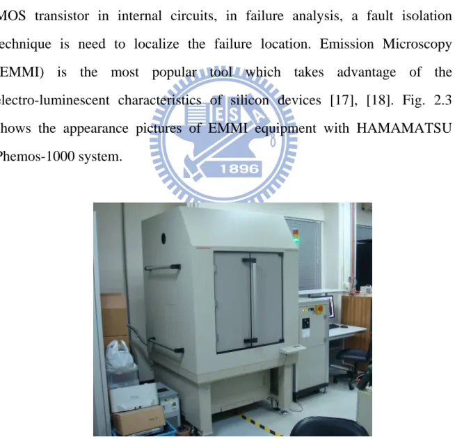
electro-luminescent characteristics of silicon devices [17], [18]. Fig. 2.3
shows the appearance pictures of EMMI equipment with HAMAMATSU
Phemos-1000 system.
For ESD FA, the evaluation of the electro-luminescent characteristics in
both forward- and reverse-biased states provides information about defects,
faults, failures, and device operation. Photons are generated as a result of
electron–hole pair (EHP) recombination and generation. As a minority carrier
recombines with the majority carrier, a photon is emitted in EHP
recombination. Additionally, photon emission can be used to find oxide and
dielectric failures. The CDM ESD events can introduce “pin hole” defects.
Oxide defects can be observed by using electro-luminescent techniques. Fig.
2.4 shows the diagram of EMMI operation principle.
CCD Detector I I Si-sub. Al Al V
or
Al • Leakage (Junction/Oxide) • Hot Electrons (Bulk) PhotonWhen gate oxide of MOS transistor in internal circuits is damage or
defective during CDM ESD events, the emitted photons in EHP
recombination can be detected by EMMI in failure device. The emission
detection mechanism is that electrons were injected into the gate oxide by
Fowler-Nordheim (F-N) tunnelling. The electrons in the gate oxide
conduction band can gain energy while travelling through the gate oxide and
become hot electrons. Hot electrons that reach the poly gate can either
recombine directly or produce additional electron-hole pairs in the poly,
which may subsequently recombine. The electron-hole recombination will
lead to photon emission and detected by EMMI detector.
2.3 Case Study on Chip-Level CDM ESD Damage
An input buffer fabricated in a 0.6-μm CMOS process is shown in Fig.
2.5. This chip is equipped with ESD protection circuit at its input pad, but it is
still damaged after 1000V CDM ESD test. Due to the consideration of noise
isolation between I/O cells and internal circuits, the VSS of I/O cells
(VSS_I/O) and the VSS of internal circuits (VSS_Internal) are separated in
the chip layout. After de-process the chip to poly layer, the failure site after
CDM ESD test is at the gate oxide of the NMOS (MN) in the input buffer, as
shown in Fig. 2.6 with the inspection of scanning electron microscopy (SEM).
As a result, the ESD protection device at the input pad can not efficiently
protect the gate oxide during CDM ESD stress, because there is no connection
between VSS_I/O and VSS_Internal. The CDM ESD current path which
Fig. 2.5 CDM ESD current path in an input buffer.
Fig. 2.6 SEM failure pictures of the failure site with gate oxide damage in the input NMOS (MN).
An output buffer fabricated in a 0.5-μm CMOS process is shown in Fig.
MP MN
R
I/P Pad Secondary ESD Circuit Primary ESD CircuitI
ESD Product A Product BVDD
VSS_I/O
VSS_Internal
transistor in the internal circuit that is connect to the output pad. The CDM
ESD current which damaged the gate oxide of NMOS (MN) is shown by dash
line in an output buffer circuit and a diagram of cross-sectional view in Fig.
2.7(a) and (b), respectively.
(a)
(b)
Fig. 2.7 CDM ESD current path in (a) an output buffer circuit, and (b) the diagram of cross-sectional view.
P+ N+ N+ N+
P-Well
I/O Pad I/O Pad MP MNI
ESD VDDFig. 2.8 SEM failure pictures of poly gate damage on a NMOS (MN)
transistor in the internal circuit.
From Fig. 2.9 to Fig. 2.11, there are two cases shown that the gate oxide
damages by using the EMMI to localize the failure device are also located in
the internal circuit after CDM ESD tests. In these two cases, the charges
stored in the body of chip still flow through the gate terminal of the input or
output MOS transistor in the internal circuits and damage its gate oxide
during CDM ESD stresses, even though ESD protection circuits have been
applied to the I/O pads. The pins near the corners in IC products are more
often to suffer CDM ESD events, because the corner pins are usually first
(a)
(b)
Fig. 2.9 After chip-level CDM ESD test, the failure point is located by (a) EMMI detection, and (b) SEM inspection.
Fig. 2.11 SEM failure pictures of gate oxide damage in internal circuit.
2.4 Board-Level CDM ESD Event in IC Products
In microelectronic system, IC chips must be attached to the PCB. Before
the attachment, static charges could be stored in the body of the chip or the
metal traces on the dielectric layer in the PCB. During the attachment, the
static charges originally stored in the chip and the PCB will be redistributed
[20], as illustrated in Fig. 2.12. Fig. 2.13 shows the charge redistribution
redistribution will occur. Cchip and Cboard denote the parasitic capacitances of
IC chip and the printed circuit board (PCB), respectively. Cchip and Cboard are
not connected in the beginning. When the IC chip is attached to the PCB, Cchip
and Cboard are shorted. Consequently, the voltages across Cchip and Cboard will
become
(2.1)
after they are connected together. The instantaneous current during the
attachment of IC chip to PCB will be significantly increased if the initial
voltage difference between the IC chip and PCB is larger. The peak current
during the charge redistribution can easily damage the IC to cause a
CDM-like failure. After the chip is attached to the PCB, certain pins in the
PCB may be connected to low potential or accidentally grounded during
module function test, as illustrated in Fig. 2.14. In this situation, the charges
originally stored in the chips and PCB will be quickly discharged through the
grounded pin to damage the chips on the PCB. If the voltages across the
equivalent capacitances of the chips and PCB are larger, more charges are
stored, which leads to larger discharging current.
board chip board board chip chip Final C C V C V C V
Fig. 2.12 Charges stored in the PCB and the charges stored in chip will be redistributed when the chip is attached to the PCB.
Fig. 2.13 When two capacitors with different voltages are shorted, charge redistribution will occur.
C
chipC
boardIC IC
Printed Circuit Board (PCB)
C
chipC
board
Fig. 2.14 When a certain pin of the PCB is grounded during the module function test, huge current will flow from the PCB through the IC to the external ground.
C
chipC
board IC IC IC External GroundCHAPTER 3
CHIP-LEVEL AND BOARD-LEVEL CDM ESD
TESTS ON IC PRODUCTS
Recently, it was informed from the IC industry that some IC products
which already passed the component-level ESD specifications were still
damaged by the CDM-like ESD events in the field applications. Besides, it
had been reported that the customer-returned ESD damages can be duplicated
by the board-level CDM ESD test [11], [12]. Some studies which evaluated
the discharging current under different charged board dimensions in the
board-level CDM ESD tests for different IC applications had been reported
[21], [22]. Board-level CDM ESD event often causes the ICs to be damaged
after the ICs are installed to the circuit boards of electronic systems. For
example, board-level CDM ESD events often occur during the module
function test on the circuit board of electronic system. Even though the IC has
been designed with good chip-level ESD robustness, it could have a reduced
ESD level in board-level CDM ESD event.
The reason is that the discharging current during the board-level CDM
ESD event is significantly higher than that during the chip-level CDM ESD
event. The board-level CDM ESD issue becomes more important in the
real-world applications of IC products which are fabricated in nanoscale
CMOS processes with the much thinner gate oxide. In this chapter, three
kinds of PCBs are used to compare the equivalent board capacitances (CB),
discharging current waveforms, and peak discharging currents under
layer is employed to perform the board-level CDM ESD tests on the test circuits fabricated in 0.25-m and 130-nm CMOS processes.
The electrostatic discharge (ESD) transient currents and failure analysis
(FA) between chip-level and board-level charged-device-model (CDM) ESD
tests are also investigated in this chapter. The discharging current waveforms
of three different printed circuit boards (PCBs) are characterized first. Then,
the chip-level and board-level CDM ESD tests are performed to an ESD
testkey of GGNMOS, an ESD-protected dummy NMOS, and a high-speed
receiver front-end circuit, respectively. Optical beam induced resistance
change (OBIRCH) is using to detect and localize the failure sites. Scanning
electron microscope (SEM) failure pictures show that the board-level CDM
ESD test causes much severer failure than that caused by the chip-level CDM
ESD test.
3.1 Measurement Setup
A CDM ESD test system, Oyrx CDM Orion, was used for field-induced
chip-level and board-level CDM ESD tests. The equipment picture is as Fig.
3.1 shown. The experimental setups of chip-level and board-level CDM ESD
tests are shown in Fig. 3.2 and Fig. 3.3, respectively. In the traditional
chip-level CDM ESD test, only the IC chip (DUT) is put on the charging plate
packaged test circuit can be mounted on the PCB to perform the board-level
CDM ESD test.
Fig. 3.1 The non-socket CDM tester (Oyrx CDM Orion). Discharge
probe L bracket
Discharge
Insulator
Fig. 3.2 Measurement setup of field-induced chip-level CDM ESD test.
Insulator Test Board Device Under Test Pogo Probe Top Ground Plane Insulator Device Under Test Pogo Probe
Top Ground Plane
Three different two-layer PCBs were chosen to investigate their board
capacitances (CB), because the board capacitance is a key factor in board-level
CDM ESD tests. The characteristics of these three PCBs are listed in Table
3.1. The board capacitances and discharging current waveforms were
monitored by Agilent 4275A LCR meter at 1 MHz and Tektronix 680C
oscilloscope, respectively, as Fig. 3.4 and Fig. 3.5 shown.
Table 3.1 Characteristics of three different kinds of PCBs.
Fig. 3.4 The LCR meter which is used for the measurement of capacitance (Agilent 4275A).
Fig. 3.5 The high-frequency oscilloscope (TDS 680C).
3.2 Experimental Results and Discussion
3.2.1 Board-Level CDM ESD Current Waveforms in Different
PCBs
Because the board capacitance (CB) is a key factor in board-level CDM
ESD tests, the higher capacitance and the higher ESD discharging energy,
three PCBs with different effective area of top plate are used to get which one
has the largest capacitance. As Fig. 3.6 shown, the larger area of top plate will
contribute the larger board capacitance (CB). Due to the area limitation of
bottom plate, 15 X 15 cm, the top plate is designed to with the area of the
same as bottom plate. Table 3.1 lists the measured board capacitance and peak
discharging current among these three PCBs under +500V and +1000V
charged voltages. Fig. 3.7, 3.8, and 3.9 show their corresponding discharging
current waveforms under +500V charged voltage. Higher peak currents were
Fig. 3.6 The top plate of board capacitance (CB) is connected to the
GND plate of PCB. The bottom plate of CB is the charging
plate of CDM ESD tester.
Charging Plate (Bottom Plate)
PCB
C
BDischarging Pin
GND Plate ( Top Plate ) GND
Fig. 3.7 Discharging current waveform of PCB_1 under +500V charged voltage.
Ipeak =5.71A
Charged Voltage = +500V
Fig. 3.9 Discharging current waveform of PCB_3 under +500V charged voltage.
3.2.2 Test With ESD Testkey of Grounded Gate NMOS
(GGNMOS)
As shown in Fig. 3.10 and 3.11, the ESD protection device GGNMOS
fabricated in a 0.25-um CMOS process was used as the test circuit. The gate
and source terminals of the GGNMOS are connected to the GND. The drain
Single finger width = 15 um
Clearance from SAB edge to ploy edge = 0.3 um
Fig. 3.11 Test circuit of ESD testkey with GGNMOS for chip-level and board-level CDM ESD tests.
In the board-level CDM ESD test with PCB_3, the bottom layer of PCB_3
was connected to the test system as the charging plate, whereas the top layer
was connected to the ground node of the test circuit. The tested pin under
CDM ESD tests is the input pad. The measured results on the chip-level and
board-level CDM ESD robustness of the GGNMOS are listed in Table 3.2.
The GGNMOS passes +2000V for chip-level and board-level CDM ESD tests.
The result indicates that the GGNMOS has high ESD robustness of chip-level
and board level CDM tests.
Table. 3.2 Chip-level CDM and board-level CDM ESD robustness of GGNMOS. GND D I/P Pad G S V ZAP Leakage current measurement
Fig. 3.12 shows the discharging current path during chip-level and board
level CDM tests. In chip-level CDM test, the discharging current flows from
bulk Si to drain input pad due to the lowest resistance path. Similarly, the
discharging current flows from source (GND) to drain input pad under
board-level CDM test. Thus, the GGNMOS is not the suitable ESD protection
device to compare the difference of chip-level and board-level CDM events.
Fig. 3.12 Discharge current path of GGNMOS under CDM ESD test.
3.2.3 Test With Dummy Receiver NMOS (RX_NMOS)
As shown in Fig. 3.13, the dummy receiver NMOS (RX_NMOS)
fabricated in a 130-nm CMOS process was used as the test circuit. The gate
terminal of the RX_NMOS is connected to the input pad to emulate the
connection of a typical input NMOS in a receiver. The drain, source, and bulk
ESD clamp NMOS. The equivalent capacitance between the input pad and
substrate of the RX_NMOS in the 40-pin DIP package is ~ 6.8 pF.
Fig. 3.13 Test circuit of RX_NMOS (dummy NMOS) for chip-level and board-level CDM ESD tests.
In the board-level CDM ESD test with PCB_3, the bottom layer of PCB_3
was connected to the test system as the charging plate, whereas the top layer
was connected to the ground node of the test circuit. The tested pin under
CDM ESD tests is the input pad. The discharging current waveforms under
+200V chip-level and +200V board-level CDM ESD tests are shown in Fig.
3.14(a) and 3.14(b), respectively. Input PAD
VSS
VDD
MP MNPower-Rail ESD Clamp Circuit
MNESD R C RX_NMOS DP DN
(a)
(b)
Time (5ns/div.) Time (1ns/div.)
As compared with the chip-level CDM ESD test, larger charging
capacitance exists in the board-level CDM ESD test. Thus, the board-level
CDM ESD test has higher peak discharging current, which results in lower
ESD robustness of the IC. The peak discharging currents and measured results
on the chip-level and board-level CDM ESD robustness of the RX_NMOS
are listed in Table 3.3. The RX_NMOS passes +200V chip-level CDM ESD
test, but fails at +200V board-level CDM ESD test. This result demonstrates
that the board-level CDM ESD robustness is lower than the chip-level CDM
ESD robustness, because the board-level CDM ESD event has much larger
discharging current than that in the conventional chip-level CDM ESD event.
Table 3.3 Chip-level CDM and board-level CDM ESD robustness of RX_NMOS.
By using the optical beam induced resistance (OBIRCH) detection, as Fig.
3.15 shown, the failure sites caused by CDM ESD test were detected and
located at the gate of the RX_NMOS. Fig. 3.16 shows the SEM failure
pictures. The test samples were de-layered to the substrate layer so the
damages at the gate oxide can be clearly observed. Comparing to Fig. 3.16(a)
and 3.16(b), the ESD damage caused by board-level CDM ESD event is much
worse than that caused by the chip-level CDM ESD event, because the
board-level CDM ESD event has much higher discharging energy than that of
Fig. 3.15 OBIRCH pictures show the failure sites caused by CDM ESD test were detected and located at the gate of the RX_NMOS.
Drai Source Source Drai Source Source I/P VSS I/P VSS
3.2.4 Test With 2.5-GHz High-Speed Receiver Interface
Circuit
A 2.5-GHz differential high-speed receiver interface circuit fabricated in a
0.13-um CMOS process was also verified with the chip-level and board-level
CDM ESD tests. Fig. 3.17 shows the circuit schematic of the 2.5-GHz
differential high-speed receiver interface circuit with on-chip ESD protection
design. The differential receiver interface circuit has the differential input
stage realized by MOS transistors. The double-diode ESD protection scheme
is applied to each differential input pad, and the P-type substrate-triggered
silicon-controlled rectifier (P-STSCR) [21] is used in the power-rail ESD
clamp circuit. Because of the high-speed application, the dimensions of ESD
diodes under the input pads are limited to reduce the parasitic capacitance at
the pads. The equivalent capacitance between the Vin pad and the substrate of
the ESD-protected 2.5-GHz differential high-speed receiver interface circuit
in a 40-pin DIP package is ~ 5.4pF.
Fig. 3.17 Test circuit of 2.5-GHz high-speed receiver interface circuit for chip-level and board-level CDM ESD tests.
Besides, a reference high-speed receiver interface circuit without on-chip
ESD protection circuit was also fabricated in the same process to compare
their ESD robustness. The tested pin under CDM ESD tests is the Vin pad.
The measured chip-level and board-level CDM ESD levels of the 2.5-GHz
high-speed receiver circuits with and without on-chip ESD protection circuits
are listed in Tables 3.4 and 3.5, respectively. The chip-level and board-level
CDM ESD levels of the reference high-speed receiver interface circuit are
quite poor, which fail at ±100V and ±50V, respectively. With the on-chip
ESD protection circuits, the failure voltages of the high-speed receiver circuit
during chip-level and board-level CDM ESD tests can be greatly improved to
-1300V and -900V, respectively. Similarly, the board-level CDM ESD level
is lower than the chip-level CDM ESD level. Failure analysis was performed
on the ESD-protected high-speed receiver interface circuits after -1300V
chip-level CDM ESD test and -900V board-level CDM ESD test.
Table. 3.4 Chip-level CDM ESD robustness of 2.5-GHz high-speed receiver interface circuit.
Table. 3.5 Board-level CDM ESD robustness of 2.5-GHz high-speed receiver interface circuit.
The SEM failure pictures after chip-level and board-level CDM ESD tests
are shown in Figs. 3.18 and 3.19, respectively. The failure points are located
at the P+/N-well ESD diode DP1. Although the ESD protection devices are
successfully turned on during CDM ESD tests, the huge current during CDM
ESD tests still damages the ESD protection devices. According to the SEM
failure pictures, the failure is much worse after board-level CDM ESD test
than that after chip-level CDM ESD test. This result has confirmed again that
board-level CDM ESD events are more critical than chip-level CDM ESD
events.
Fig. 3.18 SEM failure picture of the failure points on 2.5-GHz high-speed receiver front-end circuit after -1300V chip-level CDM ESD test.
Failure Points
DP1 MP MN DN1
Fig. 3.19 SEM failure picture of the failure points on 2.5-GHz high-speed receiver front-end circuit after -900V board-level CDM ESD test.
Failure Points
DP1 MP MN DN1
3.3 Summary
Since the board capacitance is much larger than the IC chip capacitance,
the board-level CDM ESD event has higher discharging energy than that of
chip-level CDM ESD event. Thus, the board-level CDM ESD robustness is
lower than the chip-level CDM ESD robustness. Failure analysis on the IC
samples shows that ESD damage caused by board-level CDM ESD is much
worse than that caused by chip-level CDM ESD. This result indicates that the
board-level CDM ESD event is more critical than the chip-level CDM ESD
event to IC products in field applications. The test standard on board-level
CDM ESD event should be established for IC industry to verify ESD
robustness of their IC products in real-world applications.
Recently, one draft of board-level CDM ESD test standard has been
suggested, as shown in http://proj.moeaidb.gov.tw/sipo/files/Tec/Board-Level
_CDM_Standard.pdf. We can follow this suggested board-level CDM ESD
CHAPTER 4
CONCLUSIONS AND FUTURE WORKS
4.1 Main Results of This Thesis
The chip-level and board-level CDM ESD issues in IC products are
investigated in this thesis. And based on the failure analysis result of several
case studies on chip-level CDM ESD events, the possible failure or damage
sites on ESD protection device during CDM ESD events are characterized
and summarized.
The mechanism of board-level CDM ESD event is also introduced here.
Based on this mechanism, an experiment has been performed to investigate
the board-level CDM ESD current waveforms under different sizes of PCBs
and charged voltages in the discharging path. Experimental results have
shown that the discharging current strongly depends on the PCB size and the
charged voltage. Moreover, chip-level and board-level CDM ESD levels of
several test devices and test circuits fabricated in CMOS processes have been
characterized and compared. Test results have confirmed that the board-level
CDM ESD level of the test circuit is lower than the chip-level CDM ESD test,
which indicates that the board-level CDM ESD event is more critical than the
chip-level CDM ESD event. In addition, failure analysis reveals that the
4.2 Future Works
In nanoscale CMOS processes, the gate oxide of MOS transistor becomes
thinner, which degrades the CDM ESD robustness of CMOS ICs. Moreover,
the die size becomes larger in SoC applications, so more charges will be
stored in the body of the chip. Consequently, CDM ESD issues, including
chip-level and board-level CDM ESD events, will become more critical and
should be taken into consideration in the ICs and microelectronic systems,
especially when they are realized in nanoscale CMOS processes. Since the
board-level CDM ESD damages are easily mistaken for EOS damages and no
effective design against board-level CDM ESD events was reported so far, the
formal board-level CDM ESD test standard and method should be considered
and developed. Moreover, due to the threat of the board-level CDM ESD
event in real-world failures, the test standard of board-level CDM ESD should
REFERENCES
[1] Q. Zhang, G. Peng, X. Gao, and C. Hamilton, “Failure analysis of EOS damage case study,” in Proc. of Int. Symp. on Physical and Failure Analysis of Integrated Circuits, 2009, pp. 373–376.
[2] Electrostatic Discharge (ESD) Sensitivity Testing – Human Body Model (HBM), EIA/JEDEC Standard Test Method 5.1, 2001.
[3] Electrostatic Discharge (ESD) Sensitivity Testing – Machine Model (MM), EIA/JEDEC Standard Test Method 5.2, 1999.
[4] Electrostatic Discharge (ESD) Sensitivity Testing – Charged Device Model (CDM), EIA/JEDEC Standard Test Method 5.3.1, 1999.
[5] Y. Fukuda, S. Ishiguro, and M. Takahara, “ESD protection network evaluation by HBM and CPM,” in Proc. Int. Symp. EOS/ESD, 1986, pp. 193–199.
[6] J. Stathis and D. DiMaria, “Reliability projection for ultra-thin oxides at low voltage,” in Proc. Int. Electron Devices Meeting, 1998, pp. 167–170.
[7] C. Leroux, “Analysis of oxide breakdown mechanism occurring
during ESD pulse,” in Proc. IEEE Int. Reliability Physics Symp., 2000, pp. 276–282.
[8] M.-D. Ker, W.-Y. Lo, C.-M. Lee, C.-P. Chen, and H.-S. Kao, “ESD protection design for 900-MHz RF receiver with 8-kV HBM ESD robustness,” in Proc. IEEE Radio Freq. Integrated Circuit Symp., 2002, pp. 427–430.
[9] M.-D. Ker, “Whole-chip ESD protection design with efficient
VDD-to-VSS ESD clamp circuits for submicron CMOS VLSI,” IEEE Trans. Electron Devices, vol. 46, no. 1, pp. 173–183, Jan.
transistors,” IEEE Trans. Electron Devices, vol. 49, no. 12, pp. 2171–2182, Dec. 2002.
[11] A. Olney, B. Gifford, J. Guravage, and A. Righter, “Real-world charged board model (CBM) failures,” in Proc. EOS/ESD Symp., 2003, pp. 34–43.
[12] J.-C. Tseng, C.-T. Hsu, C.-K. Tsai, S.-C. Chen, and M.-D. Ker, “Board level ESD of driver ICs on LCD panel,” IEEE Trans. on Device and Materials Reliability, vol. 9, no. 1, pp. 59–64, Mar. 2009.
[13] W. Greason, “Analysis of the charge transfer of models for
electrostatic discharge (ESD) and semiconductor devices,” IEEE Trans. Ind. Applicat., vol. 32, pp. 726–734, May/June 1996.
[14] J. Vinson and J. Liou, “Electrostatic discharge in semiconductor devices: An overview,” in Proc. IEEE, vol. 86, pp. 399–418, Feb. 1998.
[15] C. Duvvury and A. Amerasekera, “Advanced CMOS protection
device trigger mechanisms during CDM,” in Proc. Int. Symp. EOS/ESD, 1995, pp. 162–174.
[16] S. Dabral and T. Maloney, Basic ESD and I/O Design. New York: Wiley, 1998.
[17] Y.-Y. Liu, J.-M. Tao, S.-H. Chan, C.-H. Phang, and W.-K. Chim, “A new spectroscopic photon emission microscope system for semiconductor device analysis,” in Proc. of Int. Symp. on Physical and Failure Analysis of Integrated Circuits,1995, pp. 60–65.
[18] W.-K. Chim, Semiconductor Device and Failure Analysis: Using Photon Emission Microscopy. Chichester: John Wiley & Sons, Ltd, 2001.
[19] M. Tanaka and K. Okada, “CDM ESD test considered phenomena
of division and reduction of high voltage discharge in the environment,” in Proc. EOS/ESD Symp., 1996, pp. 54–61.
ESD issue in IC products,” IEEE Trans. on Device and Materials Reliability, vol. 8, 2008, pp. 694–704.
[21] J. Paasi, H. Salmela, P. Tamminen, and J. Smallwood, “ESD
sensitivity of devices on a charged printed wiring board,” in Proc. EOS/ESD Symp., 2003, pp. 143–150.
[22] T. Reinvuo, T. Tarvainen, and T. Viheriakoski, “Simulation and physics of charged board model for ESD,” in Proc. EOS/ESD Symp., 2007, pp. 318–322.