國立交通大學
電子工程學系 電子研究所
碩 士 論 文
應用於三維可程式化閘陣列之
熱感知擺放演算法
Thermal-Aware Placement for 3D FPGAs
研 究 生:許蜜祐
指導教授:黃俊達 博士
應用於三維可程式化閘陣列之
熱感知擺放演算法
Thermal-Aware Placement for 3D FPGAs
研究生:許蜜祐 Student: Mi-Yu Hsu
指導教授:黃俊達教授 Advisor: Juinn-Dar Huang
國立交通大學
電子工程學系 電子研究所
碩士論文
A Thesis
Submitted to Department of Electronics Engineering & Institute of Electronics College of Electrical & Computer Engineering
National Chiao Tung University in Partial Fulfillment of the Requirements
for the Degree of Master
in
Electronics Engineering & Institute of Electronics
October 2010
Hsinchu, Taiwan, Republic of China
應用於三維可程式化閘陣列之
熱感知擺放演算法
研究生:許蜜祐 指導教授:黃俊達教授
國立交通大學
電子工程學系 電子研究所碩士班
摘 要
三維積體電路利用垂直堆疊的方式使得摩爾定律(Moore’s Law)得以延 續,因此在近年來被廣泛討論。然而三維積體電路能降低因傳導而造成的功率, 卻存在著功率密度(power density)驟升,並連動提高溫度的隱憂。精確的溫度 分析十分耗時,但卻很難直接整合進擺放階段(placement)中。因此,此論文針 對三維可程式化閘陣列(FPGA)架構提出兩種熱感知擺放演算法-標準差法 (Standard Deviation)和踩地雷法(Minesweeper),兩者皆以分散區塊分布來降低 熱點(hotspot)的產生。標準差法以晶片上不同區域的平均使用率為基準,降低 各區域間使用率的差異;踩地雷法則是減少區塊周圍的擁擠程度,使其均勻分 布。實驗結果顯示,在可接受的線長與延遲增加範圍內,兩個方法皆可降低平均 9%的最高溫度、81%的溫度標準差和 67%的最大溫度梯度。而踩地雷法因具有快 速的更新方式,執行時間只需增加 3.49%就可達到改善溫度的效果。我們方法可 有效把溫度問題整合入擺放階段,同時將線長跟延遲結果維持在一定的程度內。Thermal-Aware Placement for 3D FPGAs
Student: Mi-Yu Hsu Advisor: Prof. Juinn-Dar Huang
Department of Electronics Engineering & Institute of Electronics
National Chiao Tung University
Abstract
Three-dimensional (3D) integration is an attractive way to continue sustaining Moore’s Law; however, it has a critical challenge – the thermal issue. Precise thermal
analysis is time-consuming and thus it is impractical to be integrated into the placement process directly for the exploding problem size in 3D technology. In 3D ICs, one of the current trends is employing field programmable gate arrays (FPGAs) because 3D FPGAs can both integrate complex circuit designs and speed up time-to-market. Since 3D FPGAs are a type of 3D ICs, thermal issue is also important for them. In this thesis, two thermal-aware placement methods for 3D FPGAs are proposed – Standard Deviation (SD) and Minesweeper (MS), which are devoted to disperse block distribution to avoid hotspots. SD utilizes the concept that minimizes the standard deviation of utilization for different parts on the chip; the idea of MS comes from minesweeper, which is to reduce the congestion of neighbors for every block. The experimental results show that improve more than 9% in maximum temperature, 81% in temperature deviation and 67% in maximum temperature gradient compared to thermal-unaware placement method with acceptable extra wire length and delay. Moreover, MS takes only 3.49% runtime overhead due to its simplified update steps. These two methods integrate efficiently thermal behavior into placement process while keeping the quality of the results good enough.
Acknowledgment
這次論文能夠完成,得力於很多人的幫助,如果沒有他們的支持與幫忙, 我沒有辦法完成這篇論文。首先要感謝我的指導教授,黃俊達老師,謝謝老師 細心且耐心的教導我,老師盡心盡力的指導讓我成長很多,老師在研究上認真 的態度是學生最良好的示範。還有謝謝我的口試委員林永隆老師、黃婷婷老師 和張世杰老師不吝於給我指導和建議,老師們專業的意見是相當寶貴的,能讓 我了解研究上面應該注意的地方。還有李育民老師,在當初第一次跟老師見 面,老師就非常熱心的給予我豐富的意見,這些資訊如果自己慢慢學習是會比 較困難的,很感謝老師百忙之中撥空來給我第二次的意見。 再來要感謝我的父母,謝謝他們培育我和陪伴我渡過寫論文的種種難關, 很感謝爸爸陪我多次的聊天給我很多鼓勵跟意見。還有要感謝雅詩和嘉怡學 姐,如果沒有他們無私的幫忙,指點我許多寫論文及做投影片的方法,不管是 哪個方面,學姐們教了我很多做研究的做法,很感謝學姐在我踏入社會之前給 予我這麼完整的指導,謝謝家宏學長、宛嫺學姐、步青學長、詣航學長、奕帆 學長,還有我的同學,揚翔和寶鑑,學弟崇羽、瀚元、哲瑋和晧凌,以及陳宏 明實驗室的柏丞學長、俊凱學長、篤雄學長、時穎學長、睿斌學長、宗穎學長、 尊宇學姐、泓懌學長和敬雨學姐,我的同學奕蓉、琬婷和佳蕙。在研究所我學 到很多也獲得很多,我非常的感激大家。Content
Abstract (Chinese) ... i
Abstract (English) ... ii
Content ... iii
List of Tables ... vi
List of Figures ... vii
Chapter 1 Introduction ... 1
Chapter 2 Preliminaries... 5
2.1 3D FPGA Architecture ... 5
2.2 3D FPGA Backend Tools ... 6
2.3 Problem Formulation ... 7
Chapter 3 Temperature Observations with Block Distribution ... 9
3.1 Thermal Model ... 9
3.2 The Influence of Patterns on Temperature ... 11
3.3 The Influence of Utilization on Temperature ... 12
3.4 The Influence of Vertical Direction Staggers on Temperature ... 14
Chapter 4 Proposed Thermal-Aware Placement ... 16
4.1 Standard Deviation (SD) Method ... 16
4.1.1 Concept – SD ... 16 4.1.2 Cost Function – SD ... 18 4.1.3 Drawbacks of SD Method ... 19 4.2 Minesweeper (MS) Method ... 20 4.2.1 Concept – MS ... 20 4.2.2 Cost Function – MS... 23
4.3 Comparisons between SD and MS ... 25
Chapter 5 Experiments ... 27
5.1 Environmental Setup ... 27
5.2 Experimental Results ... 28
5.2.1 Temperature ... 29
5.2.2 Wire Length and Delay ... 33
5.2.3 Runtime ... 35
Chapter 6 Conclusion ... 37
List of Tables
Table 1 Pattern observations ... 12
Table 2 Utilization observations ... 14
Table 3 Stagger observations in vertical direction ... 15
Table 4 Comparisons between SD and MS ... 26
Table 5 Benchmarks ... 27
Table 6 The average and maximum improvements of temperature in all cases ... 29
List of Figures
Figure 1 Relative delay vs. process technology. ... 1
Figure 2 A TSV-based 3D structure. ... 3
Figure 3 2D FPGA architecture ... 5
Figure 4 3D FPGA architecture ... 6
Figure 5 Basic flow chart of TPR and 3D MEANDER ... 7
Figure 6 3D FPGA architectural definition. ... 8
Figure 7 A typical single-chip package ... 10
Figure 8 Thermal-electrical duality. ... 10
Figure 9 Grid-based model. ... 11
Figure 10 Utilization observations ... 13
Figure 11 Two types of stagger observations in vertical direction ... 15
Figure 12 An example for grid-based and window-based standard deviation ... 17
Figure 13 An example for SD cost function. ... 18
Figure 14 An example for SD cost function update. ... 19
Figure 15 An example for concept of minesweeper. ... 20
Figure 16 An example for concept of MS cost function ... 21
Figure 17 An example for concept of MS update ... 22
Figure 18 An example for MS cost function ... 23
Figure 19 An example for MS cost function update. ... 24
Figure 20 An example for correction of MS update ... 25
Figure 21 Experimental flow. ... 28
Figure 22 The improvements of maximum temperature. ... 30
Figure 23 The improvements of temperature deviation ... 30
Figure 25 Utilization vs. temperature deviation ... 32
Figure 26 The improvements of maximum temperature gradient. ... 33
Figure 27 Extra wire length. ... 34
Figure 28 Extra delay. ... 34
Chapter 1 Introduction
The rapid scaling of silicon technology has reached great success to sustain Moore’s Law in the past decades. However, as the transistor size shrinks, physical limitations may gradually be approached and several challenges in integrated circuit design become more serious, such as power dissipation, reliability, leakage power, clock distribution and yield issue [1]. Moreover, interconnect delay has become bottleneck of chip performance [2]. As shown in Figure 1 with the size scaling down, interconnect delay grows sharply and gate delay continues to shrink. The interconnect delay dominates the system performance on chip. Hence, a solution is proposed to continue increasing transistor densities and to improve circuit performance by reducing interconnect delay in recent years, that is, three-dimensional integration [3]–[8].
Three-dimensional integrated circuits (3D ICs) use technology of stacking multiple dies together and have several advantages compared to the conventional 2D implementation. By stacking dies together, 3D ICs can have smaller footprint area
with higher transistor densities. Smaller footprint area leads to shorter global interconnect length, which causes lower power dissipation and shorter global interconnect delay. Moreover, 3D ICs enable higher heterogeneous integration on the same chip, which leads to a true system-on-a-chip.
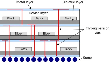
In order to stack dies together, two methods to accomplish communication links between different layers in vertical direction have been discussed in recent years [4]–[8]. The wire bonding method is preferred in the system-in-package (SiP) process [4][5] among the state-of-the-art 3D integration. However, it has some drawbacks. Inter-layer connection takes longer communication path between devices since devices only can use the outside wires to communicate. The wire bonding method also has difficulties for highly vertical connections by the limitations of the number of pins. The other method uses through-silicon vias (TSVs) [6]–[8] for vertical links. Figure 2 shows a typical TSV-based 3D IC structure. TSVs cut through thinned silicon substrates to accomplish inter-die connections so the number of pins is unlimited. This feature also allows the length of communication path between devices shorter and thus leads to shorter interconnect delay. Therefore, the performance of TSV method is better than the one of wire bonding method in general cases and TSV method is attractive in academia and industries.
Compared with application specific integrated circuits (ASICs), FPGAs have several advantages, such as faster time-to-market, simpler design cycle and more suitable for low-volume products. However, a drawback for FPGAs is larger amount of total wire length. Since 3D ICs can have higher transistor densities, 3D FPGAs can both integrate complex circuit designs and speed up time-to-market. Moreover, 3D ICs provide communication paths in vertical direction, and thus the fact helps reducing the requirement for longer interconnections, which leads to total wire length reduction. Therefore, it is valuable to develop 3D FPGAs.
Although 3D integration has a lot of advantages compared to the 2D implementation, there are still some challenges, such as immature manufacturing technology, yield issue and the most important one, thermal issue. The thermal issues are exacerbated in 3D integration for mainly three reasons: i) Higher power density – stacking many dies vertically causes the extremely increase for power density [9][10]. ii) Longer dissipation path – Except for the nearest layer from heat sink, increased thickness leads to longer heat dissipation path which causes poor heat dissipation. iii) Lower thermal conductivity of the dielectric inter-layer – the thermal conductivity of the dielectric layers inserted between device layers for insulation is very low compared to silicon and metal. All of the above aggravate thermal problems and increase temperature rapidly. Elevated temperature faces reliability [11][12] and longer wire delay problems. Therefore, the thermal issues need to be considered during every stage of 3D ICs designs, including the placement process.
There are several researches on thermal-aware placement for 3D ICs. [13][14] use partitioning-based placement method, which takes thermal issue into considerations with net weighting or cell weighting and finds mincut partitioning. [15]–[17] use force directed placement method, which usually formulate thermal problems in one of the forces. [18] uses SA-based placement method, which treats
Block Block Block
Block Block Block Block Metal layer Device layer Dieletric layer Bump Through-silicon vias
temperature minimization as part of the objective function. There are also some researches on thermal-aware placement for 2D FPGAs [19]–[22]. However, none of them target on 3D FPGAs.
To the best of our knowledge, only the approach in [23] considers thermal issues on 3D FPGAs, which is modified from a 3D FPGA CAD tool called 3D MEANDER [24][25]. However, the thermal-aware SA-based placement method is just the preprocess for routing. Placement and routing methods both pay effort to minimize total net power consumption. In placement process, SA engine encourages the length of a net with high switching activity as short as possible. However, the method ignores spatial correlation between hotspots. In other words, it may arrange two nets with high switching activity aside and create hotspots. Moreover, it does not report maximum temperature and temperature deviation and the problem sizes of benchmarks are relatively small.
In this thesis, we take thermal issues into consideration during placement process targeting on 3D FPGAs. Two SA-based placement methods effectively reduce maximum temperature, temperature deviation and maximum temperature gradient with a few extra runtime, wire length and delay compared to a thermal-unaware placement method. The remainder of this thesis is organized as follows. Chapter 2 includes preliminaries about 3D FPGA architecture, 3D FPGA backend tool and problem formulation. In Chapter 3, some temperature observations from different types of block distribution are reported and a thermal-aware area constraint method for layers is proposed. In Chapter 4, two proposed thermal-aware placement methods and comparisons between them are discussed. Experimental results are presented in Chapter 5 and some contributions are concluded in Chapter 6.
Chapter 2 Preliminaries
2.1 3D FPGA Architecture
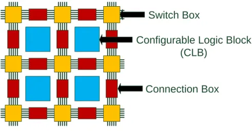
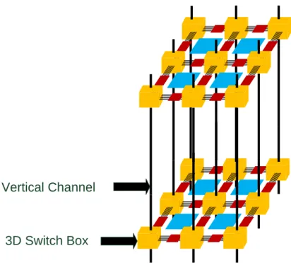
3D FPGA architecture is extended from 2D FPGA architecture, so 2D FPGA architecture is introduced first as shown in Figure 3. Configurable logic blocks (CLBs) are the basic units for FPGAs. CLBs can implement many different logic functions by programming the arrays. A connection box is a programmable switch and is used to pass signals between CLBs and wires. A switch box can change the signal direction in order to communicate CLBs in different directions or channels. In 3D FPGA architecture, for communicating with other layers, switch boxes are extended to communicate vertical direction by TSVs as shown in Figure 4.
The processes of a circuit design mapped to FPGA architecture are as follows. First, a gate-level netlist is technology-mapped into look-up tables (LUTs). Second, several LUTs are packed into a block. As the results, a gate-level netlist can be transformed into a block-level netlist. A single block can be assigned to a single CLB.
Switch Box
Configurable Logic Block
(CLB)
Connection Box
6
The goal of the placement process is finding the good assignments for all blocks with delay, wire length and temperature minimization.
2.2 3D FPGA Backend Tools
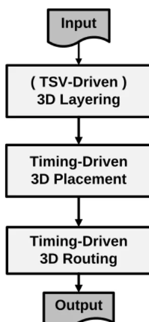
There are two backend tools targeting on 3D FPGAs. Three dimensional place and route (TPR) [26][27] is the first complete CAD flow in academia from layering process to routing process. Another existing work is called 3D MEANDER. Both of them are modified from a well known 2D FPGA CAD tool named Versatile Place and Route (VPR) [28][29]. The main flow of them is shown in Figure 5.
The first step called 3D layering is partitioning a design into different layers of 3D structure. 3D MEANDER divides a design into layer-unaware partitions and assigns each partition to different layers randomly while TPR adopts a heuristic method called EV-matrix to perform layer-aware partitioning with TSV minimization. The second step is timing-driven 3D placement. TPR and 3D MEANDER both propose SA-based placement and the objectives of placement are wire length and
3D Switch Box Vertical Channel
delay minimization. The last step is timing-driven 3D routing. If all the pins of a net are in the same layer, both the routing engines route the net with the rule that engines are forbidden using tracks in different layers. The scheme helps reducing the usage of TSVs. Both the objectives of TPR and 3D MEANDER focus on wire length and delay minimization and ignore thermal issues.
2.3 Problem Formulation
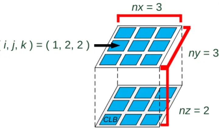
Before we start to describe our works, the definitions are shown as follows. V represents a set of blocks and E represents a set of nets. The dimensions of 3D FPGA architecture are (nx, ny, nz). CLB represents a set of CLBs. The element of CLB is denoted as clbi, j, k, clbi, j, k CLB, clbi, j, k is located at coordinate (i, j, k), i, j, k Z+,
as shown in Figure 6. Lk represents the k-th layer. block(k) is the number of blocks in
Lk and blockavg denoted as the average number of blocks in each layer is defined
as .
According to the definitions, the problem formulation is as follows. A block netlist mapped by a design and a 3D FPGA architecture with dimensions (nx, ny, nz)
nz V blockavg | | Input ( TSV-Driven ) 3D Layering Timing-Driven 3D Placement Timing-Driven 3D Routing Output
8
are given. The goal is to find a one-to-one mapping for an area balanced placement P: V (x, y, z), where x { 1, 2 … nx }, y { 1, 2 … ny }, z { 1, 2 … nz }, such that maximum temperature, temperature deviation and maximum temperature gradient are minimized with acceptable wire length, delay and runtime.
nx = 3
ny = 3
nz = 2
( i, j, k ) = ( 1, 2, 2 )
CLB
Chapter 3 Temperature
Observations with Block
Distribution
Due to the complexity, thermal analysis takes high challenges nowadays and hence it is not easy to take account of thermal effects during placement process. The current thermal models, such as finite element method (FEM) [30], finite difference method (FDM) [31] and compact resistive network [32][33], are accurate but they take minutes to analyze a design. As we know, many placement methods are iterative processes. If it takes minutes to analyze a placement for each iteration, the lack of efficiency causes the great amount of runtime. Moreover, as the technology advancing, the number of transistors in a design grows exponentially and hence problem size increases. Therefore, the demands for fast and accurate enough thermal-aware placement methods exist. We find some guidelines from temperature observations with block distribution and take them into consideration during placement process. It is helpful to simplify thermal problems and still fast enough. In this chapter, first the thermal model we used is introduced. Then the temperature observations are shown with different types of block distribution.
3.1 Thermal Model
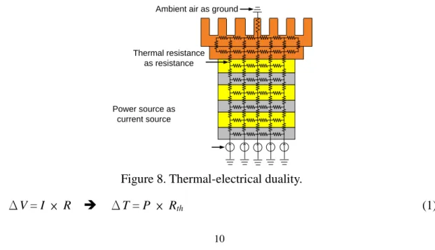
Figure 7 illustrates a typical single-chip package used by a well-known thermal model named Hotspot [32][33]. Silicon die represents the active silicon device layer and the thermal interface material layer is used to increase the efficiency and
10
uniformity of thermal transfer. Heat spreader and heat sink exhaust most of the heat. Heat generated from the active silicon device layer is delivered from the silicon die to the heat sink, and then removed to the ambient air.
According to design geometries and material physical properties, Hotspot employs thermal-electrical duality to model thermal effects at the functional block level. As shown in Figure 8, current sources (I) represent power sources (P); resistances (R) represent thermal resistances (Rth); ground represents ambient air;
voltage difference (ΔV) represents temperature difference (ΔT). The formulation of Ohm’s law for temperature is shown in (1). In Hotspot, the chip is divided into grids for analyzing thermal problems, that is, grid-based (as shown in Figure 9). The grids have different magnitude of power due to the characteristics.
ΔV = I × R ΔT = P × Rth (1) Ambient Air Heat Sink Heat Spreader Thermal Interface Material Silicon Die Power Sources
Figure 7. A typical single-chip package.
Power source as current source
Thermal resistance as resistance
Ambient air as ground
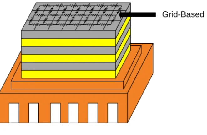
3D FPGAs has some features which can help building thermal model. First, architectural regularity of 3D FPGAs can match the grid-based characteristic for thermal analysis by dividing into grids based on CLBs. Second, the behavior inside a CLB is unknown and the two situations that can be observed from outside are occupied and unused. Therefore, occupied CLB can be denoted as holding current source and unused CLB can be denoted as open circuit. That is, the power of a CLB only has two types of magnitude. Due to the two features, the thermal problems can be treated as spatial block distributional problem.
3.2 The Influence of Patterns on Temperature
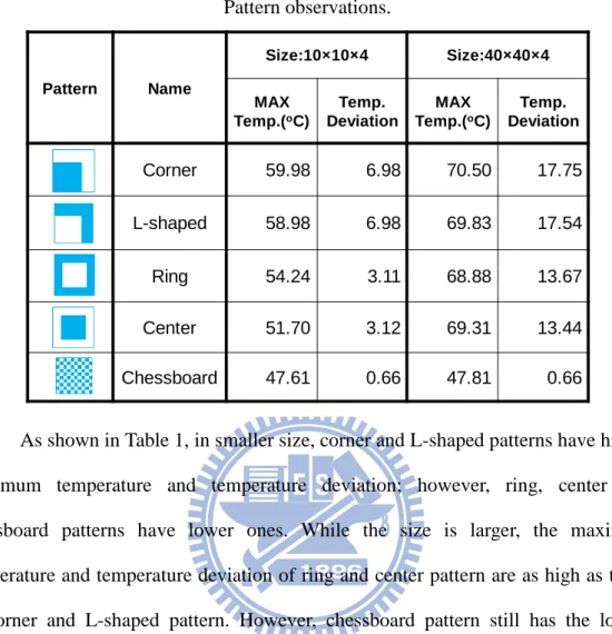
The pattern represents the planar block distribution. In this subsection, the effects of different patterns on temperature are observed. Five patterns are performed in two sizes which are 10 × 10 × 4 and 40 × 40 × 4. The utilization of all patterns is fixed to 50%. The five patterns are described as follows. i) Corner pattern – all blocks are placed on one of the corners on the chip. ii) L-shaped pattern – all blocks are placed on two sides of the chip. iii) Ring pattern – all blocks are placed on the periphery of the chip. iv) Center pattern – all blocks are placed in the center of the chip. v) Chessboard pattern – all blocks are placed evenly on the chip. The maximum temperature and temperature deviation of patterns are shown in Table 1.
Grid-Based
12
As shown in Table 1, in smaller size, corner and L-shaped patterns have higher maximum temperature and temperature deviation; however, ring, center and chessboard patterns have lower ones. While the size is larger, the maximum temperature and temperature deviation of ring and center pattern are as high as those of corner and L-shaped pattern. However, chessboard pattern still has the lowest maximum temperature and temperature deviation. Therefore, the first guideline is to assign blocks more evenly helps alleviating thermal problems.
3.3 The Influence of Utilization on Temperature
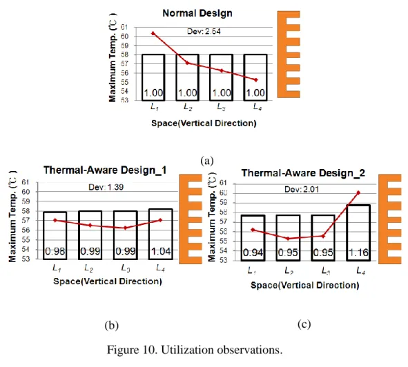
The vertical block distribution is called utilization in different layers. Because the lengths of heat dissipation path for layers are different, the utilization in layers should not be identical for better temperature profile (i.e. maximum temperature, temperature deviation and maximum temperature gradient). Different types of utilization in layers are performed as shown in Figure 10. The dimensions of the architecture are 40 × 40 × 4 and total utilization is fixed to 65%. Chessboard pattern
Table 1 Pattern observations. Pattern Name Size:10×10×4 Size:40×40×4 MAX Temp.(oC) Temp. Deviation MAX Temp.(oC) Temp. Deviation Corner 59.98 6.98 70.50 17.75 L-shaped 58.98 6.98 69.83 17.54 Ring 54.24 3.11 68.88 13.67 Center 51.70 3.12 69.31 13.44 Chessboard 47.61 0.66 47.81 0.66
is applied for each layer because of better temperature profile. Figure 10(a) shows that each layer uses the same utilization and L4 is the nearest to heat sink. The curve of
maximum temperature declines from L1 to L4, that is, the different lengths of
dissipation path for layers lead to uneven temperature distribution. Because of the result of Figure 10(a), 1%~2% blocks are moved to L4 from L1~L3 as shown in Figure
10(b). Temperature distribution in Figure 10(b) is more even. However, placing too many blocks in L4 leads to elevated temperature in L4 as shown in Figure 10(c).
Therefore, the second guideline is to place a little more blocks in the top layer, but not too many.
According to the second guideline, the thermal-aware area constraints are proposed for each layer. It is suggested to move 2% blocks from the bottom layer to the top layer at most and 1% blocks from the middle layers to the top layer at most.
Figure 10. Utilization observations.
(b) (c)
14
Besides the top layer, the number of blocks in each layer is no more than blockavg.
Using this area constraints, the temperature distribution becomes more even. The area constraint is shown in (2). lbk isdenoted as the lower bound for area constraints of Lk.
ubk isdenoted as the upper bound for area constraints of Lk. The values of lbk andubk
are shown in Table 2. ubnz represents the situation for moving the most blocks from
L1~Lnz-1 to Lnz.
blockavg × lbk block(k) blockavg × ubk (2)
3.4 The Influence of Vertical Direction Staggers on
Temperature
Another issue for vertical block distribution is the stagger between layers. We want to figure out that whether a block placed right up or down to another block causes hotspots or not. The dimensions of the architecture are 40 × 40 × 4 and total utilization is fixed to 50%. Chessboard pattern is applied for each layer for better temperature profile. Two types of observations are shown in Figure 11. Figure 11(a) is called Z-non-stagger which a block is placed right up or down to another block. Figure 11(b) is called Z-stagger opposite to Z-non-stagger. The temperature observations are shown in Table 3.
Table 2 Utilization observations. L1 L2 ... Lnz – 1 Lnz Lower Bound(lbk) 0.98 0.99 0.99 0.99 1 Upper Bound(ubk) 1 1 1 1 1+0.01nz Area Constraint Lk
The maximum temperature and temperature deviation of Z-non-stagger and Z-stagger are nearly the same. The reason is that heat sink exhausts most of the heats in vertical direction, which makes the heat dissipation in vertical direction much easier than the one in planar direction. Therefore, the third guideline is that stagger placement in vertical direction affects temperature slightly.
Figure 11. Two types of stagger observations in vertical direction. (a) Z-non-stagger (b) Z-stagger
Table 3
Stagger observations in vertical direction.
Maximum(oC) Deviation
Z-Non-Stagger 47.81 0.66
Z-Stagger 47.58 0.65
Pattern
16
Chapter 4 Proposed Thermal-Aware
Placement
As mentioned in Chapter 3, distributing block in the plane evenly can help alleviating thermal problems. The proposed thermal-aware placement methods are based on a 3D FPGA CAD tool named TPR. The original SA-based thermal-unaware placement (as shown in (3)) is modified to thermal-aware version by adding the thermal cost to the cost function as shown in (4).
Cost3D = α × Costnet + β × Costdelay (3)
Cost3D = α × Costnet + β × Costdelay + ( 1 - α - β ) × Costther (4)
Costnet is calculated by the half-perimeter bounding box of the nets. Costdelay is
computed by the delay from source to sink. The objective of the thermal cost Costther
is to achieve even block distribution in the plane. α and β are the adjustable parameters. In thermal-unaware placement, both α and β are set to 0.5. In proposed thermal-aware placement, α and β are set to 0.25.
In the rest of this chapter, two proposed thermal-aware placement methods are described. One is called Standard Deviation (SD) and the other one is called Minesweeper (MS). In the last subsection, the advantages and drawbacks of the two methods are compared.
4.1 Standard Deviation (SD) Method
4.1.1 Concept – SD
of dispersion as shown in (5). A lower standard deviation indicates that all the values are very close to the mean. Since the goal is to achieve even block distribution, standard deviation is suitable to be the cost function. Originally, a grid is used as a unit of standard deviation as shown in Figure 12(a). If a grid holds a block, the value is 1, and vice versa. In this example, 5 blocks are assigned into 9 CLBs so the average number of blocks in a grid is 5/9 = 0.56. The standard deviation of total grids is . (5 girds have 1 block and 4 grids have 0 blocks). However, no matter how the placement is changed, the standard deviation remains the same. The reason is that the total number of blocks is constant. Therefore, a grid cannot be the unit for the measure of block dispersion. The window is applied as the unit for measure as shown in Figure 12(b). A window is a square which includes several grids (more than one) on the chip and the windows in the same layer overlap with each other. If all the numbers of blocks in each window are as uniform as possible, (i.e. standard deviation is as small as possible,) the block distribution becomes more even. Since the calculation of square root is time-consuming and the value of N for each case is constant, the formulation of thermal cost can be omitted.
(5)
Figure 12. An example for grid-based and window-based standard deviation. method. 50 . 0 9 ) 56 . 0 0 ( 4 ) 56 . 0 1 ( 5 2 2 N x x x1 )2 ( 2 )2 ... ( N )2 (
18
4.1.2 Cost Function – SD
The definitions of SD cost function are as follows:
wi, j, k : The number of blocks in a window which has the lower left CLB
clbi, j, k.
win_dim : The side length of a square window.
wavg(k) : The average number of blocks in a window in Lk.
costther(k) : The thermal cost of Lk.
Costther : The total thermal cost.
According to the utilization, . costther(k) is based on
standard deviation with removing the calculation of square root and division. That is, , win_x = nx - win_dim + 1, win_y = ny - win_dim + 1. The number of windows in a layer is win_x × win_y. The total
thermal cost Costther is the summation of the thermal cost of every layer. That
is .
There is an example for SD cost function in Figure 13. The number of blocks in this layer is block(1) = 5. 2 × 2 windows are used so win_dim = 2. w1, 1, 1 = 1, w1, 2, 1
= 1, w2, 1, 1 = 2 and w2, 2, 1 = 3. According to definition, wavg(1) = 5/9 × 22 =2.22.
If nz = 1, the total thermal cost Costther = 3.63.
2 ) ( ) ( win_dim ny nx k block k wavg
nz k ther ther cost k Cost 1 ) ( 63 . 3 ) 22 . 2 3 ( ) 22 . 2 2 ( ) 22 . 2 1 ( ) 22 . 2 1 ( ) 22 . 2 ( ) 1 ( 2 2 2 2 2 1 2 1 2 , ,
i j k j i ther w cost
win x i y win j avg k j i ther k w w k cost _ 1 _ 1 2 , , ( )) ( ) ( nz = 14.1.3 Drawbacks of SD Method
The first drawback is that the calculations are too complicated. The update for moving a block to different layer is too complicated as shown in Figure 14.
In Figure 14, moving a block from L2 to L1 causes the numbers of blocks in
from-layer and to-layer changed. The number of blocks in from-layer, L2,decreases
from 7 to 6. The number of blocks in to-layer, L1,increases from 5 to 6. Accordingly,
wavg(2), wavg(1), costther(2) and costther(1) change, too. That is, all the windows in
from-layer and to-layer must be recalculated. Just moving a block to different layer leads to at least hundreds of recalculation for windows (with at least 10 × 10 windows in a layer). Moreover, the recalculations cannot be reduced in any way.
The second drawback is memory-consuming. SD has to record every wi, j, k
because moving a block from or to a window needs to update the value of wi, j, k for
the calculation of thermal cost. This inspires us to propose another efficient thermal-aware placement method.
20
4.2 Minesweeper (MS) Method
4.2.1 Concept – MS
The idea of MS comes from minesweeper. Observing minesweeper as shown in Figure 15, one of the concepts of minesweeper is that every position is calculated the number of mines in the surrounding positions. It shows that the positions of holding larger values appear in mine-gathering area. An idea comes out that counting the number of mines in the surrounding positions can represent the estimation of evenness.
An example can make this concept clear. A lot of people live together crowdedly. The probability of disturbing each other is higher. On the contrary, if people live sparsely, the probability of disturbing each other is lower. In minesweeper, if the mine distribution is uneven, the probability of counting each other is higher. As the results, the values become larger. This idea can be modeled into our thermal cost function as shown in Figure 16. Figure 16(b) is more even than Figure 16(a). The number of occupied neighbors in the surrounding positions of each block is counted. For example, the position (2, 2) in Figure 16(a) has seven occupied neighbors in the surrounding positions. Using the same idea with minesweeper, the figure also shows that the uneven pattern (Figure 16(a)) leads to appearing larger values frequently.
Then all the values are summed up from each block. For Figure 16(a), there is higher probability for double counting during the summation process. For example, because the block in position (1, 2) and the block in position (2, 2) are neighbors with each other, the value of the block in position (1, 2) and the value of the block in position (2, 2) both add one. The total values of Figure 16(a) and Figure 16(b) are 34 and 18 respectively. Larger nunber of double counting causes larger total value in the example of Figure 16(a). Therefore, the total value of the number of occupied neighbors in the surrounding positions of each block can estimate evenness. Because the unused CLBs have much lower power, there is no need to calculate the number of occupied neighbors of unused CLBs. Therefore, MS is a block-based calculation.
When moving a block, the total value needs to be updated. There is an example in Figure 17. The before total value calculated with each block is 304. The after total value calculated with each block is 294. However, there is an easy way for calculating the after total value. Since MS is block-based, we only have to focus on the positions of occupied CLBs. First, two kinds of values caused by the from-position are subtracted as shown in Figure 17(a). The two values are equal due to duality of relationship between each other. If A is the neighbor of B, B is also the neighbor of A. One of the values is the number of occupied neighbors of the from-position, i.e., 8 in this case. The other one is caused by that each neighbor of the from-position loses one
3
5
3
5
7
4
3
4
2
1
2
4
4
2
1
2
Figure 16. An example for concept of MS cost function. (a) Total = 34 (b) Total = 18
22
neighbor which is the moving block. That is, we sub 1 eight times due to eight neighbors. Then the two kinds of values caused by the to-position are added as shown in Figure 17(b). The two values are also equal due to duality. One is the number of occupied neighbors of the to-position which is 3 in this case. The other one is caused by that each neighbor of the to-position has one more neighbor which is the moving block. That is, we add 1 three times due to three neighbors. According to above, The update is 304 - 8 - 8 + 3 + 3 = 294. The update of MS is easy and fast. Moreover, there is no need to store any data for calculations.
(a) Before
(b) After
4.2.2 Cost Function – MS
The definitions of MS cost function are as follows:
h(v) : The number of occupied adjacent neighbors of block v, 0 h(v) 4.
d(v) : The number of occupied diagonal neighbors of block v, 0 d(v) 4.
costther(v) : The thermal cost of block v.
Costther : The total thermal cost.
The adjacent neighbors are different from the diagonal neighbors because the effects from the adjacent neighbors are stronger than the other ones. The inverse of distance is used as the weight to distinguish the difference. Therefore, the formulation of costther(v) is costther(v) = 1 × h(v) + 0.7 × d(v), . The total thermal cost
is the summation of all blocks, that is .
There is an example for MS cost function in Figure 18. h(v) = 4 and d(v) = 2. costther(v) = 1 × 4 + 0.7 × 2 = 5.4. Costther = 1.7 + 3.4 + 2.7 + 3.7 + 5.8 + 6.1 + 4.4 +
3.7 + 5.8 + 5.4 + 3.4 + 1.7 + 2.4 = 50.2.
V v ther ther cost v Cost ( ) 7 . 0 2 1 d
h
h
v
h
d
h
nz =124
The update function is shown as follows:
costther_to = costther_from – 2costther(vfrom) + 2costther(vto) – θ, (6)
An example is used to explain (6) as shown in Figure 19. First the costs caused by the from-position are subtracted. The cost for moving block of the from-position is costther(vfrom) = 6.1. The total cost for the neighbors of the from-position is also 6.1.
Then the costs caused by the to-position are added. The cost for moving block of the to-position is costther(vto) = 1.7. The total cost for the neighbors of the to-position is
also 1.7. Since costther_from = 69.5 and θ = 0, costther_to = 69.5 - 6.1 × 2 + 1.7 × 2
= 60.7.
θ is treated as a correction of the overestimate. costther(vto) is overestimated when
vfrom is in the surrounding positions of vto as shown in Figure 20. The reason is that
vfrom is not an actual neighbor of vto.However, when costther(vto) is calculated, vfrom is
Figure 19. An example for MS cost function update.
otherwise 0 neighbors diagonal are and if 4 . 1 neighbors adjacent are and if 2 to from to from v v v v
(a) The costs for the moving block.
(b) The costs for from and to neighbors of moving block. nz = 1
mistaken for a neighbor of vto. Therefore, θ is subtracted for correction. If the position
of vfrom is an adjacent neighbor of vto,θ = 2. If the position of vfrom is a diagonal
neighbor of vto,θ = 1.4.
As described in this subsection, MS update function is fast and easy. Moreover, there is no need for storing any data for each block. We just scan the surrounding positions of blocks for counting the number of neighbors during updating.
4.3 Comparisons between SD and MS
Five aspects of comparisons between SD and MS are discussed as shown in Table 4. SD uses windows to calculate and the number of calculations is related to the number of CLBs in SD, that is, the dimensions of the whole architecture. However, there is no need to calculate the number of neighbors of unused CLBs in MS. MS is block-based and the number of calculations is the number of blocks in MS. Moreover, the update method for MS is much easier than the one for SD. The update method for MS just needs several additive and subtractive calculations, whereas the update method for SD may need hundreds of multiplicative and subtractive calculations. Using the concept of statistics, the quality of SD is higher. Compared the update
Vfrom
Vto
Vfrom
Vto
26
methods with SD and MS, MS is much faster.
Table 4
Comparisons between SD and MS.
SD MS
Type Window-Based Block-Based
Update Complexity O(nx× ny) O(1)
QoR Very Good Good
Speed Slow Fast
Method Comparison
Chapter 5 Experiments
5.1 Environmental Setup
The algorithms are implemented in C++/Linux environment. All experiments are conducted on a workstation with an Intel Xeon 2GHz CPU and 21GB RAM. I/O pads are placed around the bottom-most layer. The architecture settings are summarized as follows: i) Use 4-layer 3D FPGAs (nz = 4). ii) Perform three kinds of utilization for experiments: 65%, 75% and 85%. iii) Fix nx and ny as the same. The values of nx and ny are .
Fifteen benchmarks come from three sources: MCNC benchmark set [34], ITC’99 benchmark set [35] and Altera [36] as shown in Table 5, which is sorted by problem sizes. All benchmarks are run five times with different random seeds and are averaged as results.
Table 5 Benchmarks.
Name # Blocks # Nets # I/Os misex3 699 1159 28 des 796 1600 501 bigkey 854 1261 426 seq 875 1458 76 apex2 939 1572 41 s298 966 1361 10 elliptic 1802 3038 245 spla 1845 2977 62 pdc 2288 3671 56 ava2_6lut 2492 4468 84 ava0_6lut 3117 6001 84 ava1_6lut 3119 5841 84 ava1_5lut 3539 6246 84 b21 10016 15714 55 fpu 12882 20078 542 utilization nz V | |
28
Figure 21 shows the experimental flow. TSV-driven 3D layering [37] is performed first. The result of layering is used for initial placement. Then three types of placement are implemented: i) Thermal-unaware placement proposed from TPR. ii) SD placement. iii) MS placement. Finally three placement methods perform timing-driven 3D routing, which is from TPR. Three placement methods are evaluated in the following subsections.
5.2 Experimental Results
Even though the thermal issue is important, wire length and delay still have to be considered. The better performance and quality are also the goals we pursued. However, for well temperature profile, block distribution needs to be dispersed to avoid hotspots, which may cause wire length and delay overhead. Moreover, there are some extra calculations for thermal cost, which increase runtime. Therefore, the discussions in the following subsections are divided into three parts: temperature, wire length and delay and the last one, runtime. In subsection 5.2.1, the improvements of
Netlist (.net) Architecture (.arch) TSV-Driven 3D Layering Thermal-Unaware Placement Timing-Driven 3D Routing Output SD Placement MS Placement
maximum temperature, temperature deviation and maximum temperature gradient are discussed. Subsection 5.2.2 shows the extra wire length and delay, which are used to demonstrate that performance and quality are still good enough. The extra runtime is presented in subsection 5.2.3 for evaluating efficiency.
5.2.1 Temperature
Figure 22 shows the improvements of maximum temperature and Figure 23 illustrates the improvements of temperature deviation. Table 6 presents the average and maximum improvements of maximum temperature and temperature deviation in all cases. The calculation of improvement described in (7) can represent how great we achieve. All results shown in the figures and table are averaged from three kinds of utilization. Generally, the larger case is, the greater improvement becomes. Since larger case has higher maximum temperature and temperature deviation, larger case has higher opportunity to reach greater improvement. The improvements for SD are greater than those for MS in each case because SD uses the concept of statistics, which leads to higher quality. The magnitude of temperature deviation improvement is greater than that of maximum temperature improvement because our methods contribute to distribute blocks evenly.
(7) % 100 _ or 1 Unaware Thermal MS SD t improvemen Table 6
The average and maximum improvements of temperature in all cases.
SD MS Maximum Temperature Improvement Average 10.80% 9.25% Maximum 14.88% 13.00% Temperature Deviation Improvement Average 86.20% 81.15% Maximum 92.43% 86.61%
30
The relationship between utilization and temperature is shown in Figure 24 and Figure 25. The calculation of improvement is the same as (7) and three kinds of
Figure 22. The improvements of maximum temperature.
utilization are shown in the same figure. For maximum temperature and temperature deviation, the results show that the lower utilization is, the greater improvement becomes generally. The reason is that the lower utilization means more unused CLBs, that is, the block distribution can be dispersed more evenly since there are more positions available. As shown in Figure 24 and Figure 25, in 65% utilization, the maximum improvement of maximum temperature in all cases is 20.78% for SD and the maximum improvement of temperature deviation is 93.58%. Our methods in lower utilization have pretty good improvements. Moreover, even in 85% utilization, the improvements of temperature deviation are still more than 65% in each case. Our methods can reach great improvements of temperature deviation even in higher utilization.
32
Figure 26 shows the improvements of maximum temperature gradient, which is the maximum difference of temperature for any two adjacent blocks. The calculation of improvement is the same as (7) and all results shown in the figures are averaged from three kinds of utilization. In all cases, the average improvement in all cases is 67.63% for SD and 74.27% for MS. The maximum improvement is 75.20% for SD and 79.37% for MS. The improvements in all cases are more than 62%. The improvements for MS are greater than those for SD in each case because SD ignores the placement in a window. However, MS has strong attempts on not assigning other blocks in the surrounding positions. The fact just matches the definition of maximum temperature gradient. Therefore, the maximum temperature gradient improvements for MS are greater than those for SD.
5.2.2 Wire Length and Delay
For better temperature profile, block distribution must be dispersed and thus there are some overheads for wire length and delay. The calculation of extra described in (8) can show how we can minimize. All results shown in the figures are averaged from three kinds of utilization. Figure 27 shows extra wire length. The difference between two methods is slight, in other words, two methods perform similar in extra wire length. The average extra wire length in all cases is 8.55% for SD and 8.75% for MS. The maximum extra wire length is 14.37% for SD and 12.26% for MS. In extra wire length, the average is no more than 9% and the maximum is less than 15%. A larger case needs more extra wire length. The reason is that larger case results in bigger footprint area; bigger footprint area leads to longer wire length potentially. Even though, the extra wire length is still acceptable in each case.
(8) % 100 1 _ or Unaware Thermal MS SD extra
34
Figure 28 shows extra delay. Two methods perform similar in extra delay. The average extra delay in all cases is 2.49% for SD and 2.76% for MS. The maximum extra delay is 6.10% for SD and 7.00% for MS. Although the block distribution is dispersed, the extra delay is no more than 7% in each case. Moreover, problem size has no relationship with extra delay. The reason is that dispersing blocks does not necessarily affect critical delay. The range of extra delay is between -1%~7%. Therefore, the extra delay is acceptable in each case.
Figure 28. Extra delay. Figure 27. Extra wire length.
5.2.3 Runtime
There are some extra calculations for thermal cost so the runtime of SD and MS is more than the thermal-unaware one. The calculation of extra is the same as (8) and all results shown in the figures are averaged from three kinds of utilization. Figure 29 shows extra runtime. The upward-sloping curve of SD shows that the runtime grows gradually. However, the curve of MS is smoother. The reason is that due to the updating methods, most of the extra runtime for MS is caused by the first calculation of the thermal cost. However, the one for SD comes from the first calculation and update. Therefore, as the problem size increases, the extra runtime becomes more. The average extra runtime in all cases is 18.98% for SD and 3.49% for MS. The maximum extra runtime is 71.60% for SD and 5.56% for MS. MS is 5 times faster than SD in average and MS is 53 times faster than SD at most as shown in Table 7. MS is much faster than SD a lot due to the updating methods.
36 Table 7 Extra runtime of SD/MS. Benchmark Extra Runtime SD/MS misex3 1.56 des 1.64 bigkey 2.18 seq 1.80 apex2 2.23 s298 2.05 elliptic 4.05 spla 4.93 pdc 3.94 ava2_6lut 3.37 ava0_6lut 10.36 ava1_6lut 4.65 ava1_5lut 7.63 b21 15.12 fpu 53.30
Chapter 6 Conclusion
The thermal issue is important in three-dimensional integration since it has been aggravated due to higher power density, longer heat dissipation path and lower thermal conductivity of inter-layer. Since 3D FPGA is a type of 3D ICs, the thermal issue is also critical for 3D FPGAs. Therefore, two thermal-aware placement methods for 3D FPGAs have been presented in this thesis. One is called Standard Deviation (SD) method. It calculates the number of blocks in a window and finds the standard deviation as thermal cost to estimate the evenness of block distribution. The other one is called Minesweeper (MS) method. We find that the number of occupied neighbors in the surrounding positions can estimate evenness, which is used as thermal cost. Because the concept of SD is from statistics, the results for SD have greater improvements of temperature. MS is much easier and faster than SD due to the way of updating calculations.
Compared to thermal-unaware placement method, SD and MS improve over 9% in maximum temperature, 81% in temperature deviation and 67% in maximum temperature gradient in average. For better temperature profile, SD and MS only increase about 9% in wire length and 3% in delay in average, which are acceptable. Since there are extra calculations for thermal cost, some extra runtime is caused. However, MS only increases runtime 3.49% in average. In the results of our works, the wire length and delay are still good enough, while the maximum temperature, temperature deviation and maximum temperature gradient have great improvements with a few extra runtime in MS. Therefore, our methods can efficiently reduce hotspots with well quality and performance.
38
Reference
[1] “International Technology Roadmap for Semiconductor,” Semiconductor Industry Association, 2005–2009.
[2] G. Metze, M. Khbels, N. Goldsman, and B. Jacob, “Heterogeneous integration,” Tech Trend Notes, vol. 12, no. 2, p. 3, 2003.
[3] B. Black, D. W. Nelson, C. Webb, and N. Samra, “3D processing technology and its impact on IA32 microprocessors,” Proc. International Conference Computer Design, 2004, pp. 316–318.
[4] R. Tummala and V. Madisetti, “System on chip or system on package?” IEEE Design Test Computers, vol. 16, no. 2, pp. 48–56, Apr.–Jun. 1999.
[5] P. H. Shiu and K. S. Lim, “Multi-layer floorplanning for reliable system-on-package,” Proc. International Symposium Circuits and System, 2004, pp. 23–26.
[6] S. Spiesshoefer, Z. Rahman, G. Vangara, S. Polamreddy, S. Burkett, and L. Schaper, “Process integration for through-silicon vias,” Journal of Vacuum Science and Technology A, vol. 23, no. 4, pp. 824–829, Jul. 2005.
[7] K. Banerjee, S. J. Souri, P. Kapur, and K. C. Saraswat, “3-D ICs: a novel chip design for improving deep submicron interconnect performance and systems-on-chip integration,” Proc. IEEE, vol. 89, no. 5, pp. 602–633, May 2001.
[8] A. W. Topol, D. C. La Tulipe, L. Shi, D. J. Frank, K. Bernstein, S. E. Steen, A. Kumar, G. U. Singco, A. M. Young, K. W. Guarini, and M. Ieong, “Three-dimensional integrated circuits,” IBM Journal of Research and Development, vol. 50, no. 4/5, pp. 491–506, Jul.–Sep. 2006.
[9] T. Y. Chiang, S. J. Souri, C. O. Chui, and K. C. Saraswat, “Thermal analysis of heterogeneous 3D ICs with various integration scenarios,” Technical Digest International Electron Devices Meeting, 2001, pp. 681–684.
[10] S. Im and K. Banerjee, “Full chip thermal analysis of planar (2D) and vertically integrated (3D) high performance ICs,” Technical Digest International Electron Devices Meeting, 2000, pp. 727–730.
[11] Y. K. Cheng, P. Raha, C. C. Teng, E. Rosenbaum, and S.-M. Kang, “ILLIADS-T: an electrothermal timing simulator for temperature-sensitive reliability diagnosis of CMOS VLSI chips,” IEEE Transactions Computer-Aided Design Integrated Circuits Systems, vol. 17, no.8, pp. 668–681, Aug. 1998.
[12] K. Banerjee, A. Mehrotra, A. Sangiovanni-Vincentelli, and C. Hu, “On thermal effects in deep sub micron VLSI interconnects,” Proc. Design Automation Conference, 1999, pp. 885–891.
[13] B. Goplen and S. Sapatnekar, “Placement of 3D ICs with thermal and interlayer via considerations,” Proc. Design Automation Conference, 2007, pp. 626–631. [14] S. Das, A. Chandrakasan, and R. Reif, “Timing, energy, and thermal performance
of three-dimensional integrated circuits,” Proc. Great Lakes Symposium VLSI, 2004, pp. 338–343.
[15] H. Yan, Q. Zhou, and X. Hong, “Efficient thermal aware placement approach integrated with 3D DCT placement algorithm,” Proc. International Symposium Quality Electronic Design, 2008, pp. 289–292.
[16] B. Goplen and S. S. Sapatnekar, “Efficient thermal placement of standard cells in 3D ICs using a force directed approach,” Proc. International Conference Computer-Aided Design, 2003, pp. 86–89.
[17] J. Cong, G. Luo, J. Wei, and Y. Zhang, “Thermal-aware 3D IC placement via transformation,” Proc. Asia South Pacific Design Automation Conference, 2007, pp. 780–785.
[18] K. Balakrishnan, V. Nanda, S. Easwar, and S. K. Lim, “Wire congestion and thermal aware 3D global placement,” Proc. Asia South Pacific Design Automation Conference, 2005, pp. 1131–1134.
[19] K. Siozios and D. Soudris, “A novel methodology for temperature-aware placement and routing of FPGAs,” Proc. IEEE Computer Society Annual Symposium VLSI, 2007, pp. 55–60.
[20] J. Jaffari and M. Anis, “Thermal-aware placement for FPGAs using electrostatic charge model,” Proc. International Symposium Quality Electronic Design, 2007, pp. 666–671.
[21] S. Bhoj and D. Bhatia, “Thermal modeling and temperature driven placement for FPGAs,” Proc. International Symposium Circuits and System, 2007, pp. 1053–1056.
[22] S. Bhoj, “Thermal aware FPGA architectures and CAD,” Proc. International Conference Field-Programmable Logic Applications, 2008, pp. 701–702.
[23] K. Siozios and D. Soudris, “A novel algorithm for temperature-aware P&R on 3D FPGAs,” Proc. International Conference on VLSI and System-on-Chip, 2008. [24] K. Siozios, K. Sotiriadis, V. F. Pavlidis, and D. Sondris, “Exploring alternative
3D FPGA architectures: design methodology and CAD tool support,” Proc. International Conference Field-Programmable Logic Applications, 2007, pp. 652–655.
[25] K. Siozios, A. Bartzas, and D. Soudris, “Architecture-level exploration of alternative interconnection schemes targeting to 3D FPGAs: a software-supported methodology,” International Journal Reconfigurable Computing, vol. 2008, Article ID 764942, 2008.
40
[26] C. Ababei, H. Mogal, and K. Bazargan, “Three-dimensional place and route for FPGAs,” IEEE Transactions Computer-Aided Design Integrated Circuits Systems, vol. 25, no. 6, pp. 1132–1140, Jun. 2006.
[27] C. Ababei, Y. Feng, B. Goplen, H. Mogal, T. Zhang, K. Bazargan, and S. Sapatnekar, “Placement and routing in 3D integrated circuits,” IEEE Design Test Computers, vol. 22, no. 6, pp. 520–531, Nov. 2005.
[28] V. Betz and J. Rose, “VPR: A new packing, placement and routing tool for FPGA research,” Proc. International Workshop on Field Programmable Logic Applications, 1997, pp. 312–322.
[29] A. Marquardt, V. Betz, and J. Rose, “Timing-driven placement for FPGAs,” Proc. International Symposium Field-Programmable Gate Arrays, 2000, pp. 203–213. [30] W. K. Chu and W. H. Kao, “A three-dimensional transient electro thermal
simulation system for IC’s,” Proc. Therminic Workshop, 1995, pp. 201–207. [31] T.-Y. Wang, Y.-M. Lee, and C. C.-P. Chen, “3D thermal-ADI: an efficient
chip-level transient thermal simulator,” Proc. International Symposium Physical Design, 2003, pp. 10–17.
[32] K. Skadron, M. R. Stan, K. Sankaranarayanan, W. Huang, S. Velusamy, and D. Tarjan, “Temperature-aware microarchitecture: modeling and implementation,” ACM Transactions Architecture Code Optimization, vol. 1, no.1, pp. 94–125, Mar. 2004.
[33] W. Huang, S. Ghosh, S. Velusamy, K. Sankaranarayanan, K. Skadron, and M. Stan, “Hotspot: a compact thermal modeling methodology for early-stage VLSI design,” IEEE Transactions Very Large Scale Integration Systems, vol. 15, no. 5, pp. 501–513, May 2006.
[34] MCNC benchmarks. S. Yang, “Logic synthesis and optimization benchmarks user guide,” Technical Report 1991-IWLS-UG-Saeyang, 1991.
[35] ITC’99 Benchmarks. [Online]. Available:
http://www.cerc.utexas.edu/itc99-benchmarks/bench.html. [36] Altera Benchmarks. [Online]. Available:
http://www.eecs.berkeley.edu/~alanmi/benchmarks/altera/old/altera12_blif_baf.z ip.
[37] Y.-S. Huang, Y.-H. Liu, and J.-D. Huang, “Iterative 3D partitioning for through-silicon via minimization,” Proc. Workshop Synthesis and System Integration Mixed Information Technologies, 2010.
![Figure 1. Relative delay vs. process technology. [1]](https://thumb-ap.123doks.com/thumbv2/9libinfo/8464240.183299/11.892.134.753.504.979/figure-relative-delay-vs-process-technology.webp)