This content has been downloaded from IOPscience. Please scroll down to see the full text.
Download details:
IP Address: 140.113.38.11
This content was downloaded on 28/04/2014 at 07:05
Please note that terms and conditions apply.
Low-Temperature Process to Improve the Leakage Current of (Ba, Sr)TiO3 Films on
Pt/TiN/Ti/Si Substrates
View the table of contents for this issue, or go to the journal homepage for more 2000 Jpn. J. Appl. Phys. 39 L1314
(http://iopscience.iop.org/1347-4065/39/12B/L1314)
Jpn. J. Appl. Phys. Vol. 39 (2000) pp.L1314–L1316 Part 2, No. 12B, 15 December 2000
c
°2000 The Japan Society of Applied Physics
Low-Temperature Process to Improve the Leakage Current of (Ba, Sr)TiO
3Films
on Pt/TiN/Ti/Si Substrates
Chuan-Chou HWANG, Ming-Jiunn LAI, Cheng-Chung JAING1, Jyh-Shin CHEN1, Stewart HUANG2, Miin-Horng JUANG3and Huang-Chung CHENG
Department of Electronics Engineering and Institute of Electronics, National Chiao Tung University, Hsinchu, Taiwan, R.O.C.
1Precision Instrument Development Center (PIDC), National Science Council (NSC), Science-Based Industrial Park, Hsinchu, Taiwan, R.O.C. 2Mosel Vitelic Incorporation, Science-Based Industrial Park, Hsinchu, Taiwan, R.O.C.
3Department of Electronics Engineering, National Taiwan University of Science and Technology, Taipei, Taiwan, R.O.C. (Received August 21, 2000; accepted for publication October 16, 2000)
In this study, we employed an oxygen plasma post-treatment to improve the leakage characteristics of Pt/(Ba, Sr)TiO3(BST)/Pt capacitors prepared by the RF cosputtering technique. Applying oxygen plasma treatment to BST
thin films can effectively passivate the oxygen vacancies of the BST films, thus decreasing the electric conduction paths of leakage current. The leakage current is reduced by as many as two orders of magnitude by this low-temperature (250◦C) and short duration (∼5 min) process. However, the usage of oxygen plasma treatment is not unrestricted. Plasma treatment over a long time (more than 10 min) degrades the leakage characteristics, due to plasma damage. Therefore, a proper oxygen plasma treatment for as-deposited BST films is desired to improve leakage characteristics of BST thin films.
KEYWORDS: BST films, RF cosputtering, oxygen vacancies, O2plasma, low temperature
L1314
1. Introduction
Barium strontium titanate (BST) films with a high dielec-tric constant have attracted great attention for practical use in the capacitors of giga-era dynamic random-access mem-ory (DRAM).1–4)To satisfy gigabit (Gbit) generation
require-ments, BST films with considerably high dielectric constants are necessary to provide sufficient charge in a miniaturizing storage capacitor to maintain immunity against soft error5)as well as keep the cell structure simple. Other basic require-ments for BST thin films include features such as low leakage current, high breakdown electric field, high time-dependent dielectric breakdown (TDDB), and low fatigue and aging ef-fects.6, 7)
One of the most crucial issues for electrical parameters has been the leakage current of DRAM cells. Once data have been written in DRAM, charges stored in each capac-itor must maintain more than the critical amount of charges for a time interval (>DRAM refresh time) so that the infor-mation stored in each DRAM cell can be read out correctly. The operation voltage, Vcc, for Gbit DRAMs is about 2 V.
The voltage difference between two electrodes of the DRAM capacitor is 1/2Vcc (1 V). The leakage current measured at
1 V for the above-mentioned BST thin films is recognized to be dominated by the Schottky emission (SE) (electrode-limited) conduction mechanism.8–10)The SE leakage current can be affected by the metal work function of the electrodes, the oxygen vacancy accumulation at the electrode interface, and the surface morphology of the BST thin films.11–14)The
mechanism of leakage current has been ascribed to the varia-tion of the oxygen vacancies in the BST thin films.8–10, 14–17)
Recently, it was reported that the higher leakage current of BST films could be effectively reduced by activated oxy-gen annealing.14, 16, 17) However, high processing
tempera-tures (>500◦C) and long process duration (∼1 h) were nec-essary for these postannealing processes.
In this investigation, oxygen plasma treatment was per-formed on as-deposited BST films at a low substrate tem-perature (250◦C) in order to passivate the oxygen vacancies. Applying oxygen plasma treatment can provide active
oxy-gen atoms to decrease the oxyoxy-gen vacancies and improve the quality of BST films. Plasma treatments with different time intervals are also used to examine their effects on the leakage characteristics of BST thin films. In addition, the mechanism of improvements in the leakage characteristics of BST films has been investigated via various characterizations.
2. Experimental
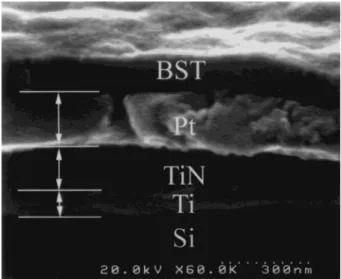
Figure 1 shows a cross-sectional scanning electron microscope (SEM) micrograph of the BST capacitor with 300◦C-deposited BST films. The structure of Pt/BST/Pt/TiN/Ti/Si was employed to simulate the practical capacitor over a bit-line (COB) DRAM capacitor structure. After a standard Radio Corporation of America (RCA) clean-ing process, Ti and TiN films with 50 and 100 nm thicknesses serving as the adhesion and the barrier layers, respectively, were sequentially deposited on the p-type Si(100) substrates by the sputtering technique. A 200-nm-thick Pt layer as the bottom electrode was also deposited by sputtering at room temperature. Accordingly, a Pt/TiN/Ti/Si substrate was
pre-Fig. 1. Cross-sectional SEM micrograph of the BST/Pt/TiN/Ti/Si for which the BST was deposited at 300◦C.
Jpn. J. Appl. Phys. Vol. 39 (2000) Pt. 2, No. 12B C.-C. HWANGet al. L1315
pared. Ba0.5Sr0.5TiO3 films, all with a nominal thickness of
100 nm, were then deposited using a RF magnetron cosput-ter system at a substrate temperature of 300◦C. To control the Ba/Sr ratio of BST thin films by tuning the RF power, BaTiO3 and SrTiO3 targets were used simultaneously. In
or-der to achieve paraelectric characteristics, the Ba/Sr ratio of 1 : 1 was selected in this investigation. The RF powers for the deposition of BaTiO3 and SrTiO3 were 175 and 230 W,
respectively.
After depositing BST films, the oxygen plasma post-treatment was performed on planar-type plasma in a 12-inch chamber for 3, 5, 10 and 15 min, to passivate the oxy-gen vacancies in various BST films. The operating conditions for the oxygen-plasma treatment are a flow rate of 900 sccm, a gas pressure of 650 mTorr, a substrate temperature of 250◦C, and a RF power of 300 W. Finally, Pt top electrodes with a diameter of 150µm were deposited on the BST films by sput-tering via a metal shadow mask process.
The composition of the resultant (Ba, Sr)TiO3 films were
analyzed by Rutherford backscattering spectroscopy (RBS). The surface morphology, the cross-sectional view, and the film thickness of the BST films were examined by scanning electron microscopy (SEM). The crystallinity and grain size estimated from the Scherrer equation were characterized by a Siemens D5000 diffractometer.18) In addition, the surface
roughness was inspected using an atomic force microscope (AFM). An automatic measurement system was conducted to obtain the current–voltage (I –V ) characteristics of the resul-tant BST capacitors.
3. Results and Discussion
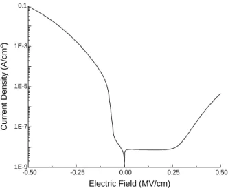
Figure 2 presents the variation of the leakage current of as-deposited BST films with applied voltage. The leakage cur-rent under reverse bias is much higher than that under positive bias. The barrier height of SE is a function of the work func-tion of the electrode metal, electron affinity of the dielectric, and the surface states. The Poole-Frenke (PF) transport mech-anism (bulk limited) results from the lowering of the barrier height of traps in the dielectrics. Hence, the PF transport mechanism does not present polarity dependence.8–10, 17)The
higher reverse current shown in Fig. 2 indicates that the leak-age current is dominated by the SE conduction mechanism
rather than the PF transport mechanism. Since the material of the top electrode is the same as that of the bottom elec-trode, the higher reverse leakage current is likely due to the high concentration of oxygen vacancies at the interface with the top electrode.8–10, 17)In order to enhance the crystallinity
and step coverage of BST films deposited by sputtering, sub-strate heating is necessary. However, as the BST films were deposited at a high substrate temperature (>300◦C), oxygen would escape and thus oxygen vacancies were generated ac-cording to:
O0↔ V++0 + 2e−+ 1/2O2,
where O0, V++0 and e−represent the oxygen ion at its normal
site, oxygen vacancy and electron, respectively. A higher con-centration of oxygen vacancies would give the BST materials n-type conductivity due to the electrons generated, causing larger leakage currents.
Since the oxygen vacancies generated during the film de-position process greatly affect the leakage characteristics, ap-plying an oxygen plasma treatment can provide active oxy-gen atoms to decrease the oxyoxy-gen vacancies and, furthermore, improve the quality of BST films. Figure 3 shows the depen-dence of the dielectric constant and the leakage current mea-sured at various electric fields on O2 plasma treatment with
different time intervals after the BST film deposition. A con-siderable reduction of the leakage current is noted in the O2
plasma-treated samples for 3, 5 and 10 min, especially that for 5 min. This improvement in leakage characteristic could be attributed to the compensation of oxygen vacancies near the surface or the improved surface roughness.13, 14)Of these two
possibilities, it was found that no obvious difference appeared in the surface roughness between the as-deposited BST films and that of samples with O2plasma treatment for 5 min. On
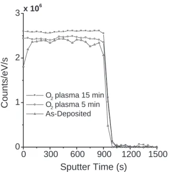
the other hand, judging from the Auger electron spectroscopy (AES) profiles, the samples with oxygen plasma treatment ex-hibited a larger amount of oxygen in the BST films than the as-deposited specimen, as shown in Fig. 4. Therefore, the improvement of leakage current at negative bias is primarily attributed to the compensation of surface oxygen vacancies. Moreover, the leakage currents in the high electric field region (0.3,−0.3 and 0.5 MV/cm) are also improved. The leakage
-0.50 -0.25 0.00 0.25 0.50 1E-9 1E-7 1E-5 1E-3 0.1
Current Density (A/cm
2 )
Electric Field (MV/cm)
Fig. 2. Variation of leakage current of as-deposited BST films with applied voltage. 0 100 200 300 Leakage Current ( A /cm 2 ) As-Depos ited Dielectric Constant 1E-7 1E-5 1E-3 0.1 O2plas ma 15 mi n O2plasma 1 0 min O2plas ma 5min O2plasma 3 min at -300 kV/cm at 500 kV/cm at -100 kV/cm at 300 kV/cm at 100 kV/cm
Fig. 3. Dependence of the dielectric constant and the leakage current mea-sured at various electric fields with a delay time of 30 s on O2 plasma treatment for different time intervals after the BST film deposition.
L1316 Jpn. J. Appl. Phys. Vol. 39 (2000) Pt. 2, No. 12B C.-C. HWANGet al.
mechanism in such a region is dominated by the PF transport mechanism.8–10, 15–17) Accordingly, the oxygen plasma treat-ment can compensate the oxygen vacancies not only on the surface but also in the bulk. The oxygen radical in oxygen plasma is so active that it can oxidize BST film and com-pensate oxygen vacancies. However, for the samples with longer plasma treatment intervals of 10 and 15 min, the leak-age current was degraded, especially in the case of the 15 min treatment, which is attributable to damage induced by plasma treatment over a long-time. The preferential crystal orienta-tion of each BST film, as checked by X-Ray Diffracorienta-tion Anal-ysis (XRD), is (110). According to the Scherrer formula, the average grain size (<100 nm) can be estimated by
D= 0.9λ/(B∗cosθ),
where D is the grain size, λ is the X-ray wavelength (∼0.15428 nm), B is the full-width at half-maximum (FWHM) of the XRD peak, andθ is the diffraction angle.18)
The FWHM of each sample analyzed by XRD is essentially identical, about 0.01725. The estimated grain size of each sample is therefore about 8.3 nm. This finding is consistent with our electrical measurements. There is no obvious differ-ence in the dielectric constant of BST films with O2 plasma
treatment of various durations, as shown in Fig. 3. Hence, proper and careful oxygen plasma treatment should be car-ried out to effectively improve the leakage characteristics of BST thin films.
4. Conclusions
The composition of BST thin films fabricated by the RF
0
300
600
900
1200 1500
0
1
2
3
x 10
6 O2 plasma 15 min O2 plasma 5 min As-DepositedCounts/eV/s
Sputter Time (s)
Fig. 4. AES profiles of the BST films without plasma post-treatment and with plasma post-treatment of 5 min, respectively.
sputtering technique shows serious oxygen deficiency, which greatly affects the leakage characteristics of the BST films. Applying oxygen plasma treatment to as-deposited BST films can effectively passivate the oxygen vacancies at low sub-strate temperatures and short process duration. Consequently, the plasma technique significantly improves the leakage cur-rents as a result of the reduction of high-concentration oxygen vacancies of the as-deposited BST films. However, plasma treatment over a long time degrades the leakage character-istics of the BST films, due to plasma damage. Therefore, proper and careful oxygen plasma treatment, after depositing the BST films, should be employed to improve the leakage characteristics of BST thin films without degradation. Acknowledgements
This work was supported in part by the Republic of China National Science Council (R.O.C. NSC) under the contract NSC-89-2215-E-009-068. Thanks are also due to the Semi-conductor Research Center (SRC) in National Chiao Tung University and the National Nano Device Laboratory (NDL) of the R.O.C. NSC for their technical support.
1) P.-Y. Lesaicherre, S. Yamamichi, H. Yamaguchi, K. Takemura, H. Watanabe, K. Tokashiki, K. Satoh, T. Sakuma, M. Yoshida, S. Ohnishi, K. Nakajima, K. Shibahara, Y. Miyasaka and H. Ono: IEDM Tech. Dig. (IEEE, Piscataway, 1994) p. 831.
2) A. Yuuki, M. Yamamuka, T. Makita, T. Makita, T. Hotikawa, T. Shibano, N. Hirano, H. Maeda, N. Mikami, K. Ono, H. Ogata and H. Abe: IEDM
Tech. Dig. (IEEE, Piscataway, 1995) p. 115.
3) S. Yamamichi, P.-Y. Lesaicherre, H. Yamaguchi, K. Takemura, S. Sone, H. Yabuta, K. Sato, T. Tamura, K. Nakajima, S. Ohnishi, K. Tokashiki, Y. Hayashi, Y. Kato, Y. Miyasaka, M. Yoshida and H. Ono: IEDM Tech.
Dig. (IEEE, Piscataway, 1995) p. 119.
4) S. Sone, H. Yabuta, Y. Kato, T. Iizuta, S. Yamamichi, H. Yamaguguchi, P.-Y. Lesaicherre, S. Nishimoto and M. Yoshida: Jpn. J. Appl. Phys. 35 (1996) 5089.
5) T. C. May and M. H. Wood: IEEE Trans. Electron Devices 26 (1979) 2.
6) T. Horikawa, N. Mikami, T. Makita, J. Tanimura, M. Kataoka, K. Sato and M. Nunoshita: Jpn. J. Appl. Phys. 32 (1993) 4126.
7) T. Kuroiwa, Y. Tsunemine, T. Horikawa and T. Makita: Jpn. J. Appl. Phys. 33 (1994) 5187.
8) W. Y. Hsu and J. D. Luttmer: Appl. Phys. Lett. 66 (1995) 2975. 9) M. S. Tsai and T. Y. Tseng: J. Electrochem. Soc. 145 (1998) 2853. 10) S. Maruno, T. Kuroiwa, N. Mikami, K. Sato, S. Ohmura, M. Kaida, T.
Yasue and T. Koshikawa: Appl. Phys. Lett. 73 (1998) 954. 11) K. Abe and S. Komatsu: Jpn. J. Appl. Phys. 33 (1994) 5297. 12) P. Bhattacharya, K. H. Park and Y. Nishhioka: Jpn. J. Appl. Phys. 33
(1994) 5231.
13) J. J. Lee, C. L. Thio and S. B. Desu: J. Appl. Phys. 78 (1995) 5073. 14) M. S. Tsai, S. C. Sun and T. Y. Tseng: J. Am. Ceram. Soc. 82 (1998)
351.
15) M. S. Tsai, S. C. Sun and T. Y. Tseng: J. Appl. Phys. 82 (1997) 3482. 16) M. S. Tsai, S. C. Sun and T. Y. Tseng: Integr. Ferroelectr. 21 (1998)
173.
17) J. H. Joo, J. M. Seon, Y. C. Jeon, K. Y. Oh, J. S. Roh and J. J. Kim: Appl. Phys. Lett. 70 (1997) 3053.
18) T. Horikawa, N. Mikami, T. Makita, J. Tanimura, M. Kataoka, K. Sato and M. Nunoshita: Jpn. J. Appl. Phys. 32 (1993) 4126.