國 立 交 通 大 學
電子工程學系 電子研究所碩士班
碩 士 論 文
二氧化鉿與氧化鋁鉿之堆疊式閘極在
金氧半場效電晶體上的特性研究
Investigation of HfO2/SiON and HfAlO/SiON
gate stack on the Characteristics of MOSFETs
研 究 生:邱大峰
指導教授:葉清發 博士
羅正忠 博士
二氧化鉿與氧化鋁鉿之堆疊式閘極在
金氧半場效電晶體上的特性研究
Investigation of HfO2/SiON and HfAlO/SiON
gate stack on the Characteristics of MOSFETs
研 究 生:邱大峰 Postgraduate:Da-Feng Chiou
指導教授:葉清發 博士 Advisor:Dr. Ching-Fa Yeh
羅正忠 博士
Dr. Jen-Chung Lou
國 立 交 通 大 學
電子工程學系 電子研究所碩士班
碩 士 論 文
A Thesis
Submitted to Department of Electronics Engineering & Institute of Electronics Engineering and Computer Science
National Chiao-Tung University in partial Fulfillment of the Requirements
for the Degree of Master of Science in
Electronics Engineering June 2007
Hsinchu, Taiwan, Republic of China
二氧化鉿與氧化鋁鉿堆疊式閘極
在金氧半場效電晶體上的特性研究
研 究 生:邱大峰 指 導 教 授:葉清發 博士 羅正忠 博士 國立交通大學 電子工程學系 電子工程所 摘 要 隨著金氧半場效電晶體尺寸的微縮,傳統的閘極介電質-二氧化矽-厚度微縮 到 1 到 1.5 奈米時,大量的漏電流將會從介電層直接穿遂過去,嚴重傷害到電晶 體的可靠度與特性,因此利用高介電常數介電質來取代傳統的二氧化矽是勢在必 行的。因為高介電常數介電質在與二氧化矽相等的等效厚度下,有較厚的實際介 電層,故可以抵擋大量的直接穿遂電流。然而,在高介電常數的介電質中所產生 的遷移率衰減與臨界電壓的不穩定都是其主要的存在問題。所以提昇驅動電流大 小並且了解高電藉常數介電質導致的可靠度下降問題都是本研究主要的探討重 點。 本論文首先探討氧化鋁鉿應用在堆疊式閘極N型金氧半場效電晶體下的特 性。經由電壓-電流與電壓-電容等圖來萃取此高介常數介電質的等效厚度。另一 部分,實驗中使用電漿增強式化學氣相沉積之氮化矽層,沉積在二氧化鉿與氧化 鋁鉿的金氧半場效電晶體上,利用較厚的氮化矽厚度會產生較大的伸張應力現象 發現N型金氧半場效電晶體之驅動電流隨著氮化矽厚度增加而增大。接著,我們也探討,二氧化鉿高介電常數介電質材料具伸張應變通道的金氧半場效電晶體, 其定電壓應力的可靠度特性分析以及偏壓變溫不穩定特性(BTI)。發現雖然較厚 的氮化矽厚度可以提升N型金氧半場效電晶體的驅動電流,但定電壓應力、偏壓 變溫不穩定特性卻在覆蓋較厚的氮化矽之電晶體下更為嚴重。特別是在高溫條件 下,氮化矽層造成的區域應力導致較多的介面狀態產生,這可能是由於通道內的 應能量造成大量矽氫鍵結斷裂。
Investigation of HfO2/SiON and HfAlO/SiON gate stack on the
Characteristics of MOSFETs
Postgraduate:Da-Feng Chiou Advisors:Dr. Chin-Fa Yeh
Dr. Jen-Chung Lou
Department of Electronics Engineering & Institute of Electronics
National Chiao Tung University
Abstract
As the conventional SiO2-based gate insulator scales down to 1.0nm~1.5nm, a large direct tunneling current generates through ultra-thin oxide which cause a serious
degradation in reliability and performance of device. Utilizing high-k dielectric to
replace SiO2-based gate as an insulator to eliminate high leakage current is necessary due to its larger physical thickness under the same equivalent oxide thickness.
However, mobility degradation and threshold voltage instability are the mainly
concern. Therefore, enhance mobility while keeping low leakage current is our aim
to realize. Beside, the reliability discussion for high-k dielectric needs to be
understood.
In this thesis, the electrical characteristics of HfAlO/SiON gate stack of
nMOSFET is discussed first. We extract the equivalent oxide thickness of HfAlO by
capacitance-voltage curve and we carried out with capping SiN layer on HfAlO/SiON
tensile strain locally in the channel region. Driving currents on nMOSFETs devices
are enhanced as the thickness of SiN layer increases due to increasing tensile strain in
the channel region. Constant voltage stress (CVS) and bias temperature (BTI)
characteristics of nMOSFET with tensile strain in the channel region are also
discussed. We can find that the nMOSFETs devices with thicken SiN capping layer
enhances drive current, the reliability concerns on CVS and BTI become huger when
thicken SiN capping layer deposited. More interface states are generated in high
CVS of nMOSFET with thicken SiN capping layer. This expresses that a higher
amount of hydrogen incorporated during SiN capping layer deposition as well as the
致謝
在兩年的碩士生涯中,首先要感謝我的指導教授羅正忠博士和葉清發博士, 由於兩位老師在研究上給予我細心的指導及教誨,讓我在學術及研究上都有莫大 的收穫。更感謝兩位老師在生活上及待人處世方面給我的幫助及啟發,讓我受益 良多並且更加成長,在這裡對兩位老師至是內心最誠摯的敬意與謝意。 此外,我要感謝我的女朋友湘淇因為有她在我背後默默支持,讓我在實驗遇 到困難及失敗時給我信心及鼓勵,讓我得以順利地完成畢業論文,也讓我碩士的 兩年生活更加的多采多姿。還有陳世璋、湯尼伯、陳永裕、紀伯翰、傅文煜、林 柏村……等諸位學長,給予我正確的研究方向並提供我實驗上的一切資源,在我 實驗遇到瓶頸時,幫助我解決困難,特別要感謝永裕學長與博翰學長在口試前一 天對我的指教,沒有你們我的論文是沒有辦法順利完成的。同時,也要感謝一起 努力的實驗室同學們:正凱(最不為人師表的教師)、建宏(每天都有可口愛心晚 餐可以吃)、宏仁(記憶體只有 1Kb 的葡萄腦)、信智(每次都愛逞強以及嘴硬)、 智仁(不管大考小考都要走天涯)、德安(最佳七舍陽光宅男),睿龍(一樣有愛心 晚餐可以吃的潮州之光)……等,跟你們相處了兩年讓我學到不少如何在遇到實 驗機台故障時的解決方法以及如何在沒經費的生活裡生存,跟你認識真的很高 興,也要感謝元愷,幸福,佳樺,土豆,岳展,嘉宏,晨修等碩一學弟感謝你們 的跑腿以及搞笑。還有很多幫助過我的人我在這裡一併的感謝你們,我會將你們 銘記在心裡。另外我要感謝國家奈米元件實驗室與交大半導體中心提供良好的設備與研究環境,讓我能順利的完成實驗。特別要感謝交大半導體中心的倪月珍小 姐,很感謝倪姐在我碩二這一年的照顧。 最後我要感謝我的家人,我可愛的妹妹俞萍,有你幫爸媽忙我可以全心的努 力研究,父親邱燕坤、母親詹桂蓮多年來辛苦的栽培與教導,提供我無憂無慮的 求學環境,並給我最大的關懷與支持。在此我獻上內心最深的謝意:爸、媽,謝 謝你們~~
Contents
Abstract (in Chinese)………I
Abstract (in English)………...III
Acknowledgement (in Chinese)……….…...V
Contents………..VII
Table Captions……….IX
Chapter 1 Introduction
1-1 Background and Motivation………1
1-2 Organization of the Thesis………...4
Chapter 2 Device fabrication and Measurement Setup
2-1 Experimental………...6.
2-2 Measurement Setup………..8
Chapter 3 Electrical Characteristics of nMOSFETs with
HfAlO/SiON gate stack
3-1 Introduction………18
3-2 Brief Review of Strained Si………20
3-3 Electrical Characteristics of MOSFETs with different thickness of SiN capping
layer………...24
3-4 Summary………....30
Chapter 4 Reliability of MOSFETs with HfO
2/SiON
4-1 Introduction………55
4-2 Brief Review of NBTI……….………57
4-3 Reliability of MOSFETs with different thickness of SiN capping layer……… 61
Chapter 5 Conclusion and Future Work
5-1 Conclusion………..…….…..79
5-2 Future Work………81
Table Captions
Table 1-1 2005 International Technology Roadmap of Semiconductor (ITRS)
Figure Captions
Chapter 2
Fig 2-1 The process flow of nMOSFET device with HfO2 and HfAlO gate stack
Fig 2-2 The cross section of nMOSFET with HfO2 and HfAlO gate stack
Fig 2-3 Configuration of charge pumping measurement setup
Fig 2-4 Configuration for (a) gate-to-substrate (Cgb) (b) gate-to-channel (Cgc) capacitance measurements
Fig 2-5 Configuration of Carrier Separation measurement setup for nMOSFET
Fig 2-6 Configuration of Carrier Separation measurement setup for pMOSFET
Fig 2-7 Configuration of CVS (constant voltage stress) measurement setup
Chapter 3
Fig 3-1 Definition of in- and out-of-plane direction
Fig 3-2 Ellipsoids of constant electron energy in reciprocal (“k”) space (a)
Unstrained Si (b) Strained Si;(c) Strain splits the energy level as shown,
removing the degeneracy between theΔ4 andΔ2
Fig 3-3 Hole constant energy surfaces at 25meV obtained from six band kp
calculations for common types of stresses:(a) unstressed, (b) longitudinal
and (d) biaxial tension
Fig 3-4 Hole intervalley phonon scattering process. High stress and splitting larger
than the optical phonon energy (60 meV) are required to suppress
scattering.
Fig 3-5 Simplified schematic of valence band splitting of strained Si as a function of
gate overdrive.
Fig 3-6 The C-V curve of the HfAlO gate stack nMOSFET
Fig 3-7 The EOT for HfAlO gate stack nMOSFET
Fig 3-8 The drain current versus to gate voltage with different SiN capping layer for
HfAlO gate stack nMOSFET
Fig 3-9 The Transconductance of devices with different capping layers for HfAlO
gate stack nMOSFET
Fig 3-10 The drain current versus to gate voltage with different SiN capping layer for
HfAlO gate stack nMOSFET
Fig 3-11 The drain current versus to gate voltage with different SiN capping layer for
HfO2 gate stack pMOSFET
Fig 3-12 The transconductance of devices with different capping layers for HfO2 gate stack pMOSFET
nMOSFET
Fig 3-14 The maximum transconductance versus to different channel length for
HfAlO gate stack nMOSFET
Fig 3-15 The drain current versus to different area for HfAlO gate stack nMOSFET
Fig 3-16 The subthreshold swing versus to different channel length for HfAlO gate
stack nMOSFET
Fig 3-17 Vth roll-off characteristics for HfAlO gate stack nMOSFET
Fig 3-18 Gate leakage current versus gate bias for fresh n-channel devices at room
temperature
Fig 3-19 Charge pump current for HfAlO gate stack nMOSFET with different SiN
thickness
Fig. 3.20 (a) In control devices, hydrogen species mainly locate at the interface to
passivate the interface states. (b) In SiN-capping devices, a large amount of
hydrogen species from the SiN layer diffuse to the gate oxide layer and the
Si/HfAlOinterface.
Fig 3-21 Carrier separation for HfAlO without SiN under (a) inversion (b)
accumulation
Fig 3-22 Carrier separation for HfAlO with SiN 1000A under (a) inversion (b)
Fig 3-23 Carrier separation for HfAlO with SiN 2000A under (a) inversion (b)
accumulation
Fig 3-24 Carrier separation for HfAlO with SiN 3000A under (a) inversion (b)
accumulation
Fig 3-25 n+-gated nMOSFET with HfAlO/SiON gate stack under inversion region
(a)Band diagrams, and (b) Schematic illustration of carrier separation
experiment.
Fig 3-26 n+-gated nMOSFET with HfAlO/SiON gate stack under accumulation
region (a) Band diagrams, and (b) Schematic illustration of carrier
separation experiment.
Fig 3-27 Gate leakage current versus gate bias without SiN for fresh n-channel
devices at various temperatures
Fig 3-28 Gate leakage current versus gate bias with SiN 1000A for fresh n-channel
devices at various temperatures
Fig 3-29 Gate leakage current versus gate bias with SiN 2000A for fresh n-channel
devices at various temperatures
Fig 3-30 Gate leakage current versus gate bias with SiN 3000A for fresh n-channel
Fig 3-31 Conduction mechanism for source/drain current fitting under inversion
region without SiN
Fig 3-32 Conduction mechanism for source/drain current fitting under inversion
region with SiN 1000A
Fig 3-33 Conduction mechanism for source/drain current fitting under inversion
region with SiN 2000A
Fig 3-34 Conduction mechanism for source/drain current fitting under inversion
region with SiN 3000A
Fig 3-35 Conduction mechanism for substrate current fitting under inversion region
without SiN
Fig 3-36 Conduction mechanism for substrate current fitting under inversion region
with SiN 1000A
Fig 3-37 Conduction mechanism for substrate current fitting under inversion region
with SiN 2000A
Fig 3-38 Conduction mechanism for substrate current fitting under inversion region
with SiN 3000A
Fig 3-39 Energy ban diagram for HfAlO/SiON gate stack to illustrate the conduction
Fig 3-40 The result of electron and hole trap with different SiN capping layer
Chapter 4
Fig 4-1 Bonding configuration at the surface of the (a) (111) Si surface and (b) (100)
Si surface.
Fig 4-2 Band diagrams of the Si substrate of a p-channel MOS device (a) negative
interface trap charge at flat-band and (b) positive interface trap charge at
inversion
Fig 4-3 Band diagrams of the Si substrate of a n-channel MOS device (a) positive
interface trap charge at flat-band and (b) negative interface trap charge at
inversion.
Fig 4-4 Id-Vg for HfO2 nMOSFETs before and after stress 1000s with and without SiN capping layer at room temperature.
Fig 4-5 Threshold voltage shift (∆Vth) as a function of stress time for HfO2 nMOSFETs without SiN.
Fig 4-6 Threshold voltage shift (∆Vth) as a function of stress time for HfO2 nMOSFETs with SiN 1000A
Fig 4-7 Threshold voltage shift (∆Vth) as a function of stress time for HfO2 nMOSFETs with SiN 2000A
nMOSFETs with SiN 3000A
Fig 4-9 Threshold voltage shift (∆Vth) as a function of stress time for HfAlO nMOSFETs withoutSiN capping layer under various temperature
Fig 4-10 Threshold voltage shift (∆Vth) as a function of stress time for HfAlO nMOSFETs with SiN 1000A capping layer under various temperature
Fig 4-11 Threshold voltage shift (∆Vth) of HfO2 nMOS as a function of stress time which compares without SiN and with SiN 3000A under CVS 1.5V and
CVS 2.5V
Fig 4-12 Gm_max degradation rate for HfO2 nMOS with different SiN thickness after CVS 1000 sec
Fig 4-13 Threshold voltage shift (∆Vth) as a function of stress time for HfAlO nMOSFETs without SiN
Fig 4-14 Threshold voltage shift (∆Vth) as a function of stress time for HfAlO nMOSFETs without SiN capping layer under various temperature
Fig 4-15 Threshold voltage shift (∆Vth) as a function of stress time for HfAlO nMOSFETs with SiN 1000A
Fig 4-16 Threshold voltage shift (∆Vth) as a function of stress time for HfAlO nMOSFETs with SiN 1000A capping layer under various temperature
nMOSFETs with SiN 2000A
Fig 4-18 Threshold voltage shift (∆Vth) as a function of stress time for HfAlO nMOSFETs with SiN 2000A capping layer under various temperature
Fig 4-19 Threshold voltage shift (∆Vth) as a function of stress time for HfAlO nMOSFETs with SiN 3000A
Fig 4-20 Threshold voltage shift (∆Vth) as a function of stress time for HfAlO nMOSFETs with SiN 3000A capping layer under various temperature
Fig 4-21 Threshold voltage shift (∆Vth) as a function of stress time for HfAlO nMOSFETs with different SiN capping layer under CVS 2V at 25℃
Fig 4-22 Threshold voltage shift (∆Vth) as a function of stress time for HfAlO nMOSFETs with different SiN capping layer under CVS 2V at 12
Fig 4-23 Gm_max degradation rate for HfAlO nMOSFETs with different SiN
Chapter 1
Introduction
1.1 Backgrounds and Motivation
According to the international technology roadmap of semiconductor (ITRS)
(Table 1-1), the metal oxide semiconductor field effect transistors (MOSFET) of high
density integration circuit and high performance, device geometry such as channel
length and thickness of gate dielectric would be reduced. However, as the
conventional gate dielectric scales down to 1.0nm~1.5nm, the viability of SiO2 will face several challenges like a large leakage current occurs through the ultra-thin oxide
by direct tunneling mechanism [1]. This phenomenon increases standby power
consumption and loss of inversion charge which degrade the reliability and
performance of device seriously. In order to suppress the leakage current and
maintain excellent performance of device, replace the conventional SiO2-based dielectric by high-k dielectric as a gate insulator is necessary. High-k dielectric can
efficiently reduce direct tunneling current through the oxide efficiently due to its high
dielectric constant. At same equivalent oxide thickness (EOT) high-k dielectric has
replacement for SiO2.
Several high-k dielectrics are investigated in the literature, among these high-k
dielectrics, Hafnium oxide (HfO2) is the most promising candidate due to its high permittivity (k ~ 20 for HfO2 ) as compared to Al2O3 and Si3N4 , high thermodynamic stability on silicon (47.6Kcal/mol at 727℃) as compared to TiO2 and Ta2O5 and its relatively high band gap (~5.8ev) among its high-k contender, appropriate barrier
height for both electrons and holes (>1ev), and compatible with poly-silicon gate
process. However, Hafnium oxide also has some challenge such as trapping in the
bulk dielectric and interfacial layer between high-k and Si-sub which cause mobility
degradation and threshold voltage instability especially in its quite low crystallize
temperature (< 500 ℃) [2-5], which restricts to the thermal budget after the post
deposition anneal (PDA) and brings about the leakage current and non-uniformity
associated with grain boundaries. By contrast, Al2O3 dielectric is an extremely promising selection on terms of its chemical, thermal stability as well as its high
barrier offset and band gap (barrier height of electron and hole are 2.9ev and 4.3ev,
band gap about 8.3ev) (Table1-2). In order to gain high dielectric constant and
thermal stability, we avoid the low crystallize temperature by adding Al to HfO2. It can be seen that the crystallize temperature increase between 500 and 600 ℃ for 6.8%
is increased further to about 31.7%, the depending crystallize temperature will
increase between 800 ~ 900 ℃, which is about 400 ℃ higher than HfO2 without Al [5].
Besides, enhanced turn-on current by tensile stress in nMOSFET is investigated.
[6] The uniaxial strain was induced by depositing SiN capping layer on HfO2/SiON
and HfAlO/SiON gate stack nMOSFET device and the magnitude of driving current
is proportion to the thickness of SiN capping layer. However, the reliability concern
such as negative bias temperature instability (NBTI) becomes worsened as compared
to thinner SiN capping layer. In this study, we analyses the characteristic and
performance of the nMOSFET device with HfAlO/SiON gate stacking structure, the
1.2 Organization of This Thesis
In this thesis, we discuss methodically the HfO2/SiON and HfAlO/SiON gate
stacking structure in terms of five chapters.
In chapter 1, we show the background and motivation respectively and the
characteristics of high-k dielectric.
In chapter 2, we explain the process flow of MOSFET device about the
HfO2/SiON and HfAlO/SiON gate stacking structure and illustrate the method of
measurement techniques.
In chapter 3, after measurement we show some basic electrical characteristics
about HfAlO with different thickness of SiN capping layer such as Id-Vg, Id-Vd, C-V,
charge pumping…etc. By these data we can verify what type interfacial layer is and
use carrier separation to obtain leakage current mechanism.
In chapter 4, we discuss the reliability issues with device that utilized
HfO2/SiON dielectric. BTI (bias temperature instability) is also an important part of
reliability issues.
In chapter 5, we summarize the important issues of this study. Some
recommendations for future works are investigated.
Year of Production 2006 2007 2008 2009 2010 2011 2012 EOT(physical) for
high-performance(nm) 1.1 1.1 1.0 1.0 0.9 0.65 0.9 Electrical thickness adjustment for
gate depletion and inversion layer effects (nm)
0.74 0.74 0.7 0.7 0.7 0.27 0.25
Normal gate leakage current
density linit(at 25oC)(A/cm2) 536 800 800 1180 1100 1560 2000
Table 1-1 2006 International Technology Roadmap of Semiconductor (ITRS)
High-κ Dielectrics
Al2O3 ZrO2 HfO2
Bandgap (eV) 8.3 5.82 6.02 Barrier Height to Si (eV) 2.9 1.5 1.6
Dielectric Constant 9 ~ 25 ~ 25 Heat of Formation (Kcal/mol) 399 261.9 271 ΔG for Reduction (MOx + Si → M + SiOx) 63.4 42.3 47.6 Thermal expansion coefficient (10-6 oK-1) 6.7 7.01 5.3 Lattice Constant (Å) (5.43 Å for Si) 4.7- 5.2 5.1 5.11
Chapter 2
Device fabrication and Measurement Setup
2.1 Experimental Details
In this section, we expound the process flow of the nMOSFET device
fabrication systematically. Local oxidation of silicon (LOCOS) was applied for
device isolation. The nMOSFET devices were fabricated on 6-inch p-type (100)
Si wafer by conventional integration process. After LOCOS formation, before
dielectric deposited, we dipped the dilute-HF about seven minutes to eliminate the
native oxide that on the active area, then we avoided the contamination of organic
element, particle and metal ion by standard RCA clean. At once, a thin interfacial
layer of SiON was formed by oxide rapid thermal anneal (RTA) at 800℃ in N2O ambient with 30 seconds and it was measured approximate 0.7 nm by ellipsometer
analysis. This film can alleviate the interfacial layer growth and prevent the leakage
current through the dielectric. And then the 30nms HfO2 and HfAlO films were deposited by atomic layer deposition (ALD) immediately. In order to improve the
dielectric film quality, following RTA at 600℃ for Hf02 and 700℃ for HfAlO with 20 seconds in N2 ambient is necessary. A 200nm poly-silicon was deposited on the dielectric by low pressure chemical vapor deposition (LPCVD) then the gate electrode
was defined by I-line stepper after I-line PR coating and etched by electron cyclotron
resonance etcher (ECR). After removing sidewall polymer by SC-1
(NH4OH:H2O2:H2O=1:1:5), S/D extension implant was done in order to avoid the hot carrier effect in the channel. A 200nm spacer formation was carried out by plasma
enhance chemical vapor deposition (PECVD) then etched by TEL5000 system.
Subsequently, S/D implantation was finished. Then definition and implantation of
body region was achieved respectively. Afterwards, the stress induced by
Si3N4/SiO2 capping layer was deposited by PECVD. In order to verify the relation between the stress effect and the thickness of Si3N4, we divided the Si3N4 thickness into four parts such as 100nm, 200nm, 300nm and without Si3N4. We obtained the magnitude of stress by stress measurement system and it showed 184.3 Mpa a for
100nm, 226.9 Mpa for 200nm and 432Mpa for 300nm. In some studies, we know
that the stress magnitude is relative to the concentration of nitrogen in Si3N4 deposition. Final, Al-Si-Cu metallization were implemented by physical vapor
deposition (PVD) system. After metal etching, forming gas annealing at 400℃ in
H2/N2 ambient for 30 minutes was used to fix dangling bond and reduces interfacial
state density. We show the process flow and the cross section of nMOSFET device
2.2 Measurement setup
Some basic electrical characteristics of the nMOSFET device such as
current-to-voltage and capacitance-to-voltage were extracted by Agilent 4156C
precision semiconductor parameter and HP 4284 LCR meter respectively.
First, we can obtain the equivalent oxide thickness of the HfAlO and HfO2 dielectric MOSFET device from the capacitance in inversion region of C-V profile
without considering quantum effect. The equation is
oxide inversion A C EOT ε = (2-1)
whereas ε, A are permittivity and device area respectively. In addition, the interface
state density (Nit) was measured by charge pumping method [7]. A series of
continuous square waveforms (f = 1 MHz) were generated and applied to gate by
8110 pulse generator while source, drain and body were grounded. Besides, we fix
the magnitude of the square waveforms at 1.5V and the base voltage was varied from
accumulation to inversion. After measurement, we gained a list of the charge
pumping current (Icp) data and calculated the Nit from the equation
Icp = q f Nit A (2-2)
whereas q, A and f are electron charge, the area of device and frequency of pulse
respectively. Fig 2-3 shows the configuration of charge pumping measurement setup.
calculated form threshold voltage shift (△Vth) by assuming that the charge was trapped at the interface between the dielectric and Si substrate. The equation is
th tot C V N qA ∆ ∆ = (2-3)
therefore, we can obtain the ∆Not (oxide trap or bulk trap) from (2-2) and (2-3) by
following equation
ot tot it
N = N - N
∆ ∆ ∆ (2-4)
However, by measuring the charge pumping current (Icp) wuth variable fall and rise times, we can obtain the energy distribution of the interface states in a relatively
huge part of the forbidden energy gap on both sides of midgap [8-9]. Interface
states act as acceptor-like or donor-like which depend on their relative state to the
band gap. Donor-like interface states are neutral when they are empty or negative
when occupied by electron. In contrast, acceptor-like states are positive when they
are empty or neutral when occupied by electron. Relative position depends on its
Fermi level and an interface trap will be occupied by an electron or empty.
Simultaneously, we listed some useful equations for analyzing whether acceptor-like
or donor-like interface states.
-2 ln ln fb t cp it r f th i n p a V V I qD AkT t t V n f V σ σ ⎡ ⎛ ⎞⎤ ⎢ ⎜ ⎟⎥ = + ⎜ ⎟ ⎢ ⎝ ⎠⎥ ⎣ ⎦ (2-5)
( - , ) ,e -- - ln i f inv E E fb th kT em i th i n f a V V E E kT V n t e V σ ⎛ ⎞ ⎜ ⎟ = + ⎜ ⎟ ⎝ ⎠ (2-6) (- - , ) , -- ln i f acc E E fb th kT em h i th i p r a V V E E kT V n t e V σ ⎛ ⎞ ⎜ ⎟ = + + ⎜ ⎟ ⎝ ⎠ (2-7)
( )
2 - ( constant) f cp it r f t dI N E t qATf dt = (2-8)( )
1 - ( constant) cp r it r r dI t N E t qATf dt = (2-9)If we gained the result that Nit(E2) was an extensive variation and Nit(E1) was almost similar according to equation (2-5), (2-6) and (2-8), we could observe that it existed
strong fall time dependence of charge pumping curve for fixed rise time. It shows
that acceptor-like interface states exist because huge interface state variation is near
conduction band. Similarly, Nit(E1) was a large variation and Nit(E2) was almost similar according to (2-5), (2-7) and (2-9), it means that it existed strong rise time
dependence of charge pumping curve for fixed fall time and donor-like interface states
exist because large interface variation is near valence band.
The electron mobility of nMOSFET was measured by split C-V method. The
effective mobility of electron was measured at low drain bias and then gave
d eff n g L WQ
µ
= (2-10)Where the Qn was measured from capacitance measurement and drain conductance gd was defined as constant GS D d V DS I g V = ∂ = ∂ (2-11)
The capacitance meter was connected between the gate and the source/drain were
connected together with the substrate grounded. Therefore, Qn was observed as follows -GS V n gs g Q = ∫∞ C dV (2-12)
And effective electric field produced by the voltage was express as
0 b n eff s Q Q E K η ε + = (2-13)
Qb was measured from capacitance measurements. The capacitance meter was
connected between the gate and substrate and the source/drain were connected
grounded together. Therefore,
VGS
b fb gb g
Q = ∫ C dV (2-14)
where Qn and Qb were charge densities in depletion layer and inversion layer respectively. The parameter η= 1/2 was for electron. And subsequently universal
mobility was accomplished by this equation
1.69 638 1 eff eff area µ ε = ⎛ ⎞ + ⎜⎝ ⎟⎠ (2-15)
We can obtain the data that we need easily from above all equation. Fig 2-4
illustrates the configuration of split C-V measurement setup.
Carrier separation measurement is shown in Fig 2-5 and Fig 2-6 for nMOSFET
of gate leakage current under different state (i.e. inversion or accumulation). By
comparing the IG, ISD and IB that we can define which path dominates the leakage mechanism.
Subsequently, in CVS measurement method, a constant voltage stress was
applied to the gate of device and the source/drain/substrate were grounded
respectively. We obtained the measurement data such as Id-Vg and charge pumping
during the stress intervals that Fig 2-5 shows the configuration of CVS measurement
setup. After analyzing these data we could observe the shift of transconductance
(Gm) and threshold voltage and charge pumping measurement is also used to
calculate the interface state generation under inversion. In the same way, we could
Standard LOCOS process
STD clean and HF dip
SiON ~ 0.7nm at 850℃ in
N
2O ambient
ALD HfO
2and HfAlO 30nm
deposited
600℃ 20sec for HfO
2700℃ 20sec for HfAlO
PDA
Poly silicon gate deposition
200nm and patterning
S/D extension and S/D implant
Dopant activation at 950℃
30sec in N
2ambient
Passivation layer deposition
Split table
100nm 200nm 300nm
Metallization
● Standard LOCOS process ● STD clean and HF dip
● SiON ~ 0.7nm at 850℃ in N2O ambient ● ALD HfO2 and HfAlO 30nm deposited
● PDA at 600℃ 20sec for HfO2 and 700℃ 20sec for HfAlO in N2 ambient ● Poly silicon gate deposition 200nm and patterning
● S/D extension and S/D implant ● Body engineering
● Dopant activation at 950℃ 30sec in N2 ambient
● Passivation layer deposition (split table: 100nm, 200nm and 300nm SiN ) ● Metallization
Fig 2-1 The process flow of nMOSFET device with HfO2 and HfAlO gate stack
Fig 2-2 The cross section of nMOSFET with HfO2 and HfAlO gate stack
Si-sub
Poly-Si
SiO
2Si
3N
4FOX
FOX
SiO
2Si
3N
4 HfAlO or HfO2S
D
Fig 2-3 Configuration of charge pumping measurement setup
Fig. 2.4 Configuration for (a) gate-to-substrate (Cgb) (b) gate-to-channel (Cgc) capacitance measurements S/D G B B G S/D
n
-n
-n
-n
-n
-n
-p
+-sub
p
+-sub
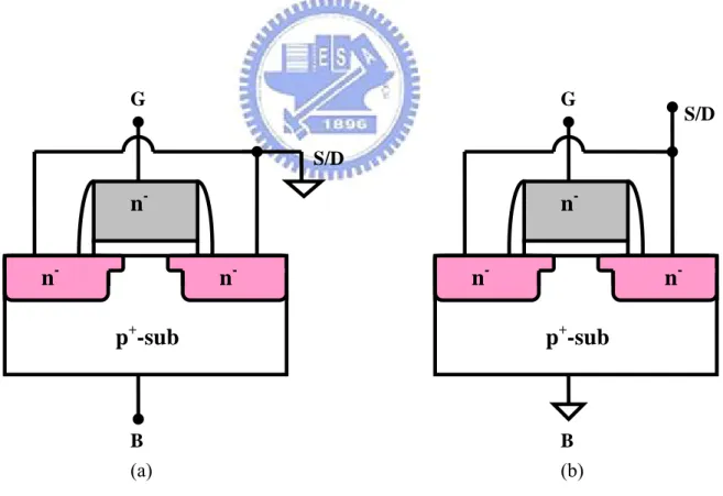
(a) (b) Switch HP 4156 GPIB p-substrate n -Source n -Drain n -Gate e -h+ HP 81110A Pulse GeneratorFig 2-5 Configuration of Carrier Separation measurement setup for nMOSFET
Fig 2-6 Configuration of Carrier Separation measurement setup for pMOSFET
S/D G B B G S/D
n
-n
-n
-n
-n
-n
-p
+-sub
p
+-sub
(a) inversion (b) accumulation Vg sweep -
~
+
Vg sweep +~
-S/D G B B G S/D
n
-n
-n
-n
-n
-p
+-sub
p
+-sub
(a) inversion (b) accumulation Vg sweep -
~
+
Vg sweep +~
-Fig 2-7 Configuration of CVS (constant voltage stress) measurement setup. P-sub n- n -n -Stress time DC stress 1sec DC stress 5sec DC stress X sec
Id-Vg Id-Vg Id-Vg
Constant stress applied to gate :
CVS=1.5, 2, 2.5, 3V for nMOS G (overwrite)
Chapter 3
Result and discussion
3.1 Introduction
Scaling of COMS has not only led to an increase of integration circuit density
but also a corresponding enhancement in the transistor performance. However,
when gate length scaled down to the nanometer order, some limitation such as gate
oxide leakage current and and power density, make geometric scaling an increasingly
challenging task. In order to continue CMOS device performance improvement, the
industry needs a new scaling vector. Starting with the 90-nm technology generation,
mobility enhancement through uniaxial process-induced strained Si has emerged as
the next scaling vector being widely adopted in logic technologies [10~12].
Strain improves MOSFET drive current by altering the band structure of the
channel. Biaxial and uniaxial strained silicon technologies are promising for
enhancement of CMOS performance [13]. Biaxial tensile strain can be done by
using a wafer-based approach of a thin strained Si layer on a thick relax SiGe virtual
substrate, however, biaxial tensile strained silicon is difficult to implement because of
some disadvantages of SiGe, such as misfit and threading dislocations, Ge
threading dislocation density (typically > 104 cm-2) of the virtual SiGe substrates represents a major obstacle for practical applications. In contrast, uniaxial strain can
easily be applied by modifying capping layer deposition [18][19], shallow trench
isolation [20][21], source/drain material [22], silicidation [23], packing process [24],
and so on. In this paper, we utilized the SiN capping layer as a stressor due to its
high stability and compatibility of conventional COMS process flow. Recently, it
has been shown that the mechanical stress from a contact etch-stop SiN layer over the
gate electrode can significantly affect the drive current [25][26]. Depending on the
deposition conditions, the SiN capping layer can generate either tensile or
compressive stress [26]. It thus can be applied to the NMOS devices that benefit from
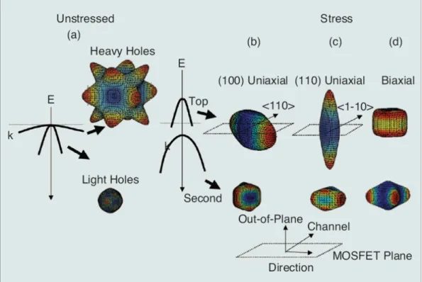
3.2 Brief Review of Strained Si
The carrier mobility is given by q*
m
τ
µ = , where 1/τ is scattering rate and m* is the conductivity effective mass. Strain enhance the mobility by reducing the
conductivity effective mass and/or the scattering rate. For electrons, both mass and
scattering rate reducing are generally accepted as important for mobility
enhancement[28]. However, for holes, only mass change due to band warping and
repopulation [29] plays a significant role at today’s manufacturable stress level (about
< 1GPa) since strain-induced valence band splitting is smaller than that for the
conduction band. Furthermore, though there has been focus on reduced in-plane mass
to increase the mobility, increasing the out-of-plane mass for electrons and holes is
also now understood to equally important factor for maintaining the mobility
enhancement at high vertical fields, Fig 3-1 shows the definition of in- and
out-of-plane. For electron transport in bulk Si at room temperature, the conduction
band consists of six degenerate valley as shown in Fig 3-2(a) and these valleys are
equal energy. The effective mass for any direction is the reciprocal of the curvature
of the electron energy function. For unstressed bulk Si, the total electron
conductivity mass, m*, is given by
-1 * 1 2 4 6 l t m m m ⎡ ⎛ ⎞ ⎛ ⎞⎤ =⎢ ⎜ ⎟ ⎜+ ⎟⎥ ⎝ ⎠ ⎝ ⎠ ⎣ ⎦
mass (perpendicular to the axis) about 0.19 mo, where mo is the free electron mass.
After stressing, the valleys of Si are shown in Fig 3-2(b). For MOSFETs on a wafer,
advantage strain removes the degeneracy between the four in-plane valley (Δ4) and the two out-of-plane (Δ2) by splitting them in energy as shown in Fig 3-2(c). The lower energy of theΔ2 valleys means that they are preferentially occupied by electron. The electron mobility partly improves via a reduced in-plane and increased
out-of-plane m* due to the favorable mass of the Δ
2 valleys, which result in more electrons with an in-plane transverse effective mass (mt =0.19 mo) and out-of-plane
longitudinal mass (ml =0.98 mo). However, electron scattering is also be reduced
due to the conduction valleys splitting into two sets of energy levels, which
suppresses the rate of intervalley phonon scattering between theΔ2 and Δ4 valleys. For holes, the valence band structure of Si is more complex than the conduction
band. Due to this complex structure as well as valence band warping under the strain
that results in a larger mobility enhancement than electron. These two factors are also
the reason that strained pMOSFET is a key focus in advantage logic technology. For
unstrained Si at room temperature, holes occupy the top two band:the heavy and light
hole bands. The unstrained constant energy surfaces for the two bands of Si are
shown in Fig 3-3(a). With the application of strain, the hole effective mass becomes
pure heavy, light, and split-off bands. Thus, the light and heavy hole bands lose their
meaning, and holes increasingly occupy the top band at higher strain due to the energy
splitting. The warped top two bands are shown in Fig 3-3(b), (c) and (d) for the
three most common types of stresses. As shown in Fig 3-3 (b) and (c), the narrow
constant energy surface in the channel direction for uniaxial compression creates a
desire mass that about 40% smaller in-plane mass as compared to biaxial tensile strain.
It is important to achieve high hole mobility by a low in-plane conductivity mass for
the top band (namely a narrow width to the constant energy surface along the channel
direction). This result is due to the difficulty of significantly enhancing hole
mobility by reducing the intervalley scattering rate. Hole intervalley scattering rate
is not significantly reduced for stress less than 1 GPa since the band splitting is less
than the optical phonon energy (60mev). Splitting is greater than 60mev and stress
is greater than 1GPa are necessary to suppress the intervalley phonon scattering rate
(see Fig 3-4). This is why the change of effective mass plays a more significant role
than reduced phonon scattering in hole mobility enhancement.
Hole mobility at high vertical field with uni-axial compressive and biaxial tensile
stresses would have different behaviors. Fig 3-5 shows the energy shift with
confinement for both uniaxial and biaxial stress. Etop represents the top band with large out-f-plane mass for uniaxial stress and small out-f-plane mass for biaxial stress
which compare to the second band, Esecond. Thus, uniaxial has a small shift in energy (indicates Etop which compares to unstrained) due to confinement for it, but there is a large shift for biaxial. As shown in Fig 3-5, the strain-induced band splitting (Etop- Esecond) increases for uniaxial strain but decreases for biaxial stress. Thus, confinement favors occupation of the top band for uniaxial compressive stress and the
second band for biaxial tensile stress. The net effect is strain and confinement
additive for uniaxial compressive stress and subtractive for biaxial tensile stress.
Thus, the competing effects of strain and confinement on band splitting is a factor of
lost hole mobility in biaxial tensile stress for pMOSFET at high vertical fields. For
uniaxial stress, the band splitting increased that maintains the hole mobility
enhancement at high vertical fields. This is why the uniaxial compressive stress is
extensively adopted in pMOSFET [12][31] [32].
For NMOSFETs, it has been reported that the threshold voltage shift caused by
bi-axial tensile stress is larger than the case with uni-axial tensile strain [33]. For
PMOSFETs, larger shift of light-hole band edge under bi-axial tensile strain leads to
larger shift in Vth, compared with the case with uni-axial compressive strain [34].
3.3 Electrical Characteristics of MOSFETs with different thickness of
SiN capping layer and materials
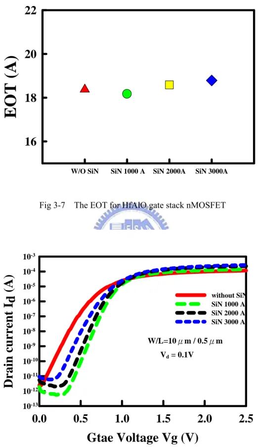
The C-V curve and EOT value are shown in Fig 3-6 and Fig 3-7 respectively, it
can be seen that the different SiN thickness which induced strain will not change the
equivalent oxide thickness of device. By this fact, we can make sure that the drive
current enhancement is not caused by EOT decrease. By equation physical ox
T EOT
κ ε= , where εox is the dielectric constant of SiO2 and Tphysical is the real thickness of gate
dielectric. Then, we can obtain that the dielectric constant,“κ”, is about 12. The
relation of Id-Vg and Gm-Vg characteristic of HfAlO gate stack nMOSFET with different SiN capping layer thickness that upon the gate are shown in Fig 3-8 and Fig
3-9. Simultaneously, the Id-Vd is also shown in Fig 3-10. It is about 2 times enhancement for Id and Gm between the without SiN and SiN 3000A. The improvement of drain current and transconductance is obviously proportional to the
thickness of SiN layers. The mechanism which results in these results might be as
follows: These SiN capping layers upon the poly-Si gates with highly tensile stress
cause the poly-Si gates under them to be with compressive strain, and then the tensile
strain is caused in the channel regions by these compressive poly-Si gates upon
channel regions. The results might also be caused by another mechanism: The SiN
regions in the two terminals of channels. These SiN layers cause the source/drain
regions under them compressive and the channel regions are implicated to become
tensile. Fig 3-11 and Fig 3-12 show that the relation of drain current and
transconductance of HfO2 gate stack pMOSFET with different tensile SiN capping layer. According to [12], it can be obtained the degradation of drain current for
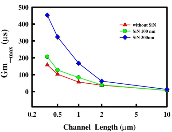
pMOSFET in such a tensile stress and it is about 14.8% and 30.8% degradation of Id and Gm respectively in figure. The relation between drain current and channel length of HfAlO gate stack nMOSFET is shown in Fig 3-13 and Gm is in Fig 3-14. By above result, we can know that the strain effect is strong with short channel especially
when channel length downs to 0.35µm. However, it can be also seen that the drain
current enhancement is saturated when channel length is above 2µm. In addition,
Fig 3-15 shows that the relation of drain current with different areas of channel, when
area of channel is large, the strain effect will not enhance the drain current. Unlike
biaxial strain, driving current improvement with uniaxial strain obviously takes place
in short channel device. This is also fit to the scaling-down demand.
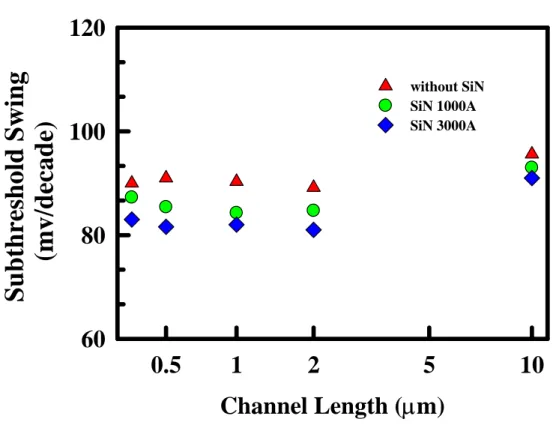
The subtreshold swing versus to channel length of HfAlO gate stack nMOSFET
with different SiN capping layer thickness is shown in the Fig 3-16. We find that the
subthreshold swing of SiN 3000A shows the better interface state than others. Thus,
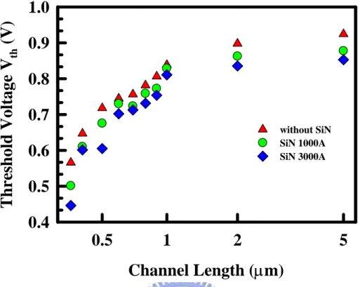
shows that the Vth roll-off characteristic with different thickness of SiN capping layer. It can be seen that when the channel length is scaled below 1µm, the roll-off
phenomenon is more series. Fig 3-18 indicates that gate leakage current seems not
to be increased as SiN thickness thicker. The extra hydrogen species come from the
SiN layer as a result of using SiH4 and NH3 as precursors during deposition. It is well known that the PE-SiN film contains a substantial amount of hydrogen [35]. Fig
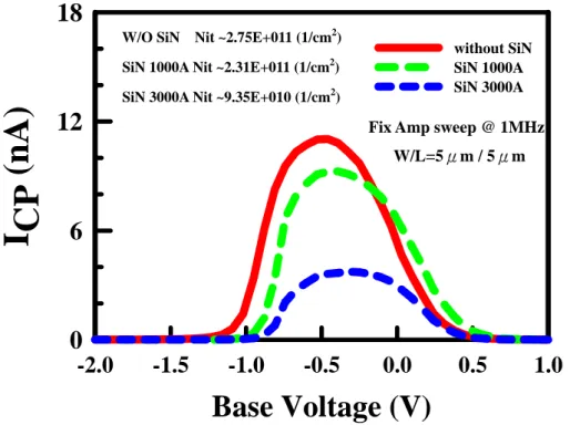
3-19 expresses the charge pumping current for different thickness of SiN layer. We
obtain that the charge pumping current decreased as the thickness of SiN capping
layer increased from 0 A to 3000 A. This means that the extra hydrogen species
come from the SiN layer as a result of using SiH4 and NH3 as precursors during deposition and a lot of dangling bond could be fixed and therefore reduced interfacial
state. It is well known that the PE-SiN film contains a substantial amount of hydrogen
[35]. These hydrogen could passivate interfacial state that located on interfacial
layer. So, depositing thicker SiN would take long time and more interfacial state
could be fixed. The brief pasivation diagram is in Fig 3-20, it can be seen that when
SiN is deposited by PECVD, a lot of hydrogen species will locate at the interface to
passivate the interface states.
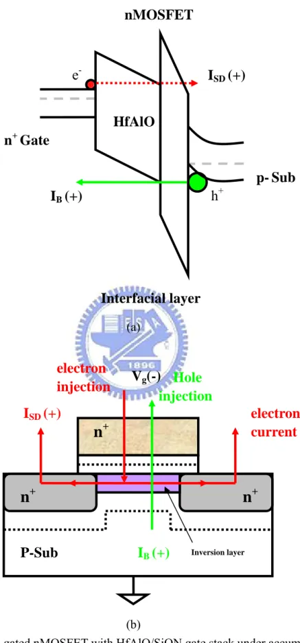
Carrier separation analysis is investigated to clarify the leakage path in gate stack
electrons. Fig 3-21, Fig 3-22, Fig 3-23 and Fig 3-24 express carrier separation
results under inversion regions and accumulation regions for n+-gate nMOSFETs with different thickness of SiN layer of HfAlO/SiON gate stack. By above result, we can
find that the IG is close to ISD under inversion region, it means that the source/drain current dominates the leakage current. In contrast, the substrate current dominates
the leakage current under accumulation region. This phenomenon indicates electron
from S/D that goes through high-k dielectric to gate is the major component of
conduction mechanism under inversion region. We can easily explain this
mechanism by band-diagram in Fig 3-25(a) and carrier separation current component
is in Fig 3-25(b). The substrate current which corresponds to hole current from the
gate, while source/drain current corresponds to electron current from silicon substrate
under inversion region. Hole supplied from gate valence band on nMOSFET are
confined by less generation of minority holes in n+-gate. In other words, carrier which go through gate dielectric are influenced by barrier height and distance[37].
Due to the asymmetry of the HfAlO/SiON (Fig 3-25(a)) and structure, we can deduce
that holes from gate electrode are hard to go through the dielectric compared to
electrons from the channel. In brief, electron current from the channel is the
predominant injection current under stressing. Similarly, the inference also is used
the band-diagram to interpret possible leakage current from under accumulation. Fig
3-26(b) shows the current component flow in carrier separation experiment. Fig
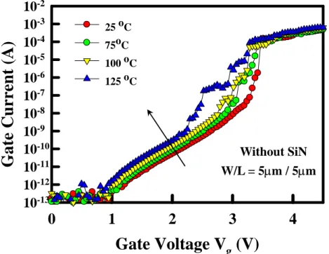
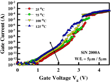
3-27, Fig 3-28, Fig 3-29 and Fig 3-30 show that the gate leakage current with different
thickness of SiN under inversion regions and these are measured form room
temperature to 125℃. We obtain the leakage current increased as temperature
elevated. This phenomenon means that the conduction mechanism must be relate
trap-related like schottky-emission, trap-assisted tunneling, Frenkel-Poole emission,
etc. Then, the result which we get accords with Frenkel-Poole emission for electron
current. Fig 3-31, Fig 3-32, Fig 3-33 and Fig 3-34 show that the excellent linearity
relation for source/drain current (electron) with different thickness of SiN under
inversion region, and Fig 3-35, Fig 3-36, Fig 3-37 and Fig 3-38 for substrate current
(hole current). Then, the fitting curve can be acquired from these dorms as follows:
2 HfAlO HfAlO 0 0 2 exp( - ) - ( - / ) * exp( ) ; , - / ) ln( )
-Intercept gives the Barrier height ( - ) B B B eff SiO eff B r B eff B B B B q a V I V T k T q qE J B E B q NT a const k T q q q J Eeff E k T k T q k T πε ε ε µ ε πε ε Φ ∝ Φ = = = = Φ = Φ ⇒
Where B is a constant which is about the trapping density and carrier mobility in
insulator, ΦB is the barrier height, Eeff is the electric field in HfAlO films,
ε
0 is the free space permittivity, kB is Boltzmann constant, and T is the temperature in Kelvin.This tendency indicates that both electron and hole conduction mechanisms
are the same, and the result agrees well with the F-P conduction mechanism. Barrier
hight ΦB and dielectric constant
ε
HfAlO of HfAlO/SiON can be calculated. The value of electron ΦB for without SiN, SiN 1000A, SiN 2000A and SiN 3000A under inversion are about 0.737eV, 0.722eV, 0.645eV and 0.621eV and ΦB for hole are 0.639eV, 0.614eV, 0.571eV and 0.464eV. The ΦB to be discussed in this chapter is the “effective” value that is representative of the HfAlO/SiON gate stack [49]. Weconsider the case when the injected carrier flow across HfAlO/SiON by hopping via
the trap sites with energy barrier ΦB, whose value depends on the fabrication process[50]. Fig 3-39 shows energy band diagram to present conduction mechanism
through HfAlO/SiON gate stack with different SiN capping layer. And Fig 3-40
shows that the result od electron and hole trap with different SiN capping layers.
3.4 Summary
In this chapter, we verify that PECVD SiN capping layer is tensile strain and
suitable for nMOSFETs application. Therefore, as SiN capping layer thickness
increases, driving current has a huge enhancement. Besides, we observe that interface
states become less when SiN capping layer thickens. It may be attributed that a large
amount of hydrogen generated from SH4 and NH3 and then passivate the interfacial layer and we verify the number of interface states by using charge pumping method.
Eventually, we utilize carrier separation method to make sure the current component
under inversion and accumulation regions and carrier separation measurement with
different temperature is followed to calculate the electron and hole barrier height
under inversion region then, we obtain F-P conduction mechanism is matched. This
`
Fig 3-1 Definition of in- and out-of-plane direction
Fig 3-2 Ellipsoids of constant electron energy in reciprocal (“k”) space (a) Unstrained Si (b) Strained Si;(c) Strain splits the energy level as shown, removing the
degeneracy between theΔ4 andΔ2
(a) (b) Kz Ky Kx
m
l Δ2 Δ4 (c) Δ2 Δ4 Δ6 in-plane Out-of-planem
tFig 3-3 Hole constant energy surfaces at 25meV obtained from six band kp calculations for common types of stresses:(a) unstressed, (b) longitudinal compression on (100) wafer (c) longitudinal compression on (110) wafer, and (d)
biaxial tension
Fig 3-4 Hole intervalley phonon scattering process. High stress and splitting larger than the optical phonon energy (60 meV) are required to suppress scattering.
Fig 3-5 Simplified schematic of valence band splitting of strained Si as a function of gate overdrive.
Gtae voltage Vg (V)
-2
-1
0
1
2
Capacitance (uF/cm
2
)
0.5 1.0 1.5 2.0 2.5 W/O SiN SiN 100 nm SiN 200 nm SiN 300 nmW/O SiN SiN 1000 A SiN 2000A SiN 3000A
EOT (A)
16
18
20
22
Fig 3-7 The EOT for HfAlO gate stack nMOSFET
Gtae Voltage Vg (V)
0.0
0.5
1.0
1.5
2.0
2.5
Drain current I
d
(A)
10-13 10-12 10-11 10-10 10-9 10-8 10-7 10-6 10-5 10-4 10-3 without SiN SiN 1000 A SiN 2000 A SiN 3000 AFig 3-8 The drain current versus to gate voltage with different SiN capping layer for HfAlO gate stack nMOSFET
W/L=10μm / 0.5μm Vd = 0.1V
Gtae Voltage Vg (V)
0.0
0.5
1.0
1.5
2.0
2.5
G
m
0
100
200
300
without SiNSiN 1000ASiN 2000A SiN 3000A
Fig 3-9 The Transconductance of devices with different capping layers for HfAlO gate stack nMOSFET
Drain voltage V
d(V)
0 1 2 3Drain curren
t I
d
(uA)
0 200 400 600 800 1000 coventional SiN 1000 SiN 2000 SiN 3000Fig 3-10 The drain current versus to gate voltage with different SiN capping layer for HfAlO gate stack nMOSFET
W/L=10μm / 0.5μm
(μ
s)
Vd = 0.1V
Gtae Voltage Vg (V)
-2.5
-2.0
-1.5
-1.0
-0.5
0.0
D
rai
n
cu
rren
t I
d
(A
)
10
-1310
-1210
-1110
-1010
-910
-810
-710
-610
-510
-410
-3 Without SiN SiN 2000 SiN 3000Fig 3-11 The drain current versus to gate voltage with different SiN capping layer for HfO2 gate stack pMOSFET
Gtae Voltage Vg (V)
-2.5
-2.0
-1.5
-1.0
-0.5
0.0
G
m
0
20
40
60
without SiNSiN 2000 ASiN 3000 A
Fig 3-12 The transconductance of devices with different capping layers for HfO2 gate stack pMOSFET
W/L=10μm / 1μm W/L=10μm / 1μm
(μ
s)
Vd = 0.1V Vd = 0.1VChannel Lengh (
µm)
0.2
0.5
1
2
5
10
I d
@ V
g
-V
t = 1 (V)
0
100
200
300
400
without SiN SiN 100 nm SiN 300 nmFig 3-13 The drain current versus to different channel length for HfAlO gate stack nMOSFET
Channel Length (
µm)
0.2
0.5
1
2
5
10
Gm
_
ma
x
(
µs)
0
100
200
300
400
500
without SiN SiN 100 nm SiN 300nmFig 3-14 The maximum transconductance versus to different channel length for HfAlO gate stack nMOSFET
L x W (
µm x µm)
0.5x10 1x10 2x10 10x10 50x50 100x100I d
(µ
A)
0
50
100
150
without SiN with SiNFig 3-15 The drain current versus to different area for HfAlO gate stack nMOSFET
Channel Length (
µm)
0.5
1
2
5
10
Subthreshold Swing
(mv/decade)
60
80
100
120
without SiN SiN 1000A SiN 3000AFig 3-16 The subthreshold swing versus to different channel length for HfAlO gate stack nMOSFET
Channel Length (
µm)
0.5
1
2
5
Threshold Voltage V
th(V)
0.4
0.5
0.6
0.7
0.8
0.9
1.0
without SiN SiN 1000A SiN 3000AFig 3-17 Vth roll-off characteristics for HfAlO gate stack nMOSFET
Gate Voltage Vg (V)
-4
-2
0
2
4
Gate Current (A)
10
-1210
-1110
-1010
-910
-810
-710
-610
-510
-4 without SiN SiN 1000A SiN 2000A SiN 3000AFig 3-18 Gate leakage current versus gate bias for fresh n-channel devices at room temperature
Base Voltage (V)
-2.0
-1.5
-1.0
-0.5
0.0
0.5
1.0
I CP
(nA)
0
6
12
18
without SiN SiN 1000A SiN 3000AFig 3-19 Charge pump current for HfAlO gate stack nMOSFET with different SiN thickness
Fix Amp sweep @ 1MHz W/L=5μm / 5μm
W/O SiN Nit ~2.75E+011 (1/cm2)
SiN 1000A Nit ~2.31E+011 (1/cm2)
(a)
(b)
Fig. 3.20 (a) In control devices, hydrogen species mainly locate at the interface to passivate the interface states. (b) In SiN-capping devices, a large amount of hydrogen
species from the SiN layer diffuse to the gate oxide layer and passivate the Si/HfAlO interface. Source Drain Gate : H species PE-Si3N4 SiO2 SiO2 Source Drain Gate : H species
Gate Voltage Vg (V)
0
1
2
3
4
C
u
rren
t (
A
)
10
-1310
-1210
-1110
-1010
-910
-810
-710
-610
-510
-4 without SiN - IG without SiN - ISD without SiN - IB (a)Gate Voltage Vg (V)
-4
-3
-2
-1
0
Current (A)
10
-1310
-1210
-1110
-1010
-910
-810
-710
-610
-510
-410
-3 without SiN - IG without SiN - ISD without SiN - IB (b)Fig 3-21 Carrier separation for HfAlO without SiN under (a) inversion (b) accumulation
Without SiN W/L=5μm / 5μ
Without SiN
Gate Voltage Vg (V)
0
1
2
3
4
Current (A)
10
-1310
-1210
-1110
-1010
-910
-810
-710
-610
-510
-410
-3 SiN 1000A - IG SiN 1000A - ISD SiN 1000A- IB (a)Gate Voltage Vg (V)
-4
-3
-2
-1
0
Current (A)
10
-1310
-1210
-1110
-1010
-910
-810
-710
-610
-510
-410
-3 SiN1000A- IG SiN 1000A - ISD SiN 1000A - IB (b)Fig 3-22 Carrier separation for HfAlO with SiN 1000A under (a) inversion (b) accumulation
W/L=5μm / 5μm W/L=5μm / 5μm
SiN 1000A
Gate Voltage Vg (V)
0
1
2
3
4
Current (A)
10
-1310
-1210
-1110
-1010
-910
-810
-710
-610
-510
-4 SiN 2000A - IG SiN 2000A - ISD SiN 2000A - IB (a)Gate Voltage Vg (V)
-5
-4
-3
-2
-1
0
Current (A)
10
-1310
-1210
-1110
-1010
-910
-810
-710
-610
-510
-410
-3 without SiN - IG without SiN - ISD without SiN - IB (b)Fig 3-23 Carrier separation for HfAlO with SiN 2000A under (a) inversion (b) accumulation
W/L=5μm / 5μm W/L=5μm / 5μm
![HPSH [ 氧化數平衡反應式係數 ]](data:image/gif;base64,R0lGODlhAQABAIAAAP///wAAACH5BAEAAAAALAAAAAABAAEAAAICRAEAOw==)