國 立 交 通 大 學
電信工程學系
碩 士 論 文
以集總與分散式元件設計任意功率分配之旁枝
耦合器
Analysis and Design of Lumped- and Distributed- Element
Branch-Line Coupler with Arbitrary Power Division
研究生:盧政良
指導教授:郭仁財博士
以集總與分散式元件設計任意功率分配之旁枝
耦合器
Analysis and Design of Lumped- and Distributed- Element
Branch-Line Coupler with Arbitrary Power Division
研究生:盧政良 Student:Zheng-Liang Lu
指導教授:郭仁財 博士 Advisor:Dr. Jen-Tsai Kuo
國立交通大學
電信工程學系
碩士論文
A Thesis
Submitted to Department of Communication Engineering
College of Electrical and Computer Engineering
National Chiao Tung University
in Partial Fulfillment of the Requirements
for the Degree of
Master of Science
in
Communication Engineering
June 2009
Hsinchu, Taiwan, Republic of China
I
以集總與分散式元件設計任意功率分配之
旁枝耦合器
研 究 生 : 盧 政 良 指 導 教 授 : 郭 仁 財 博 士
國立交通大學電信工程學系
摘要
本論文提出分析與設計方式,以集總元件實現具有寬頻、任意功
率分配之三級旁枝耦合器。藉由奇偶模分析,可知調整旁枝的傳輸線
阻抗控制旁枝耦合器的功率分配。同時,在一定的功率分配下,頻寬
的大小可以理論預測。本論文進一步利用集總與分散式元件,以縮小
三級旁枝耦合器的面積,並比較純以集總元件實現之電路和集總與分
散式元件實現之電路之間的差異。本論文實作
兩
電路,以驗證本文之
設計,量測數據與模擬結果相當一致。
II
Analysis and Design of Lumped- and
Distributed- Element Branch-Line Coupler
with Arbitrary Power Division
Student: Zheng-Liang Lu
Advisor: Dr. Jen-Tsai Kuo
Department of Communication Engineering
National Chiao Tung University
Abstract
This thesis designs a 3-section wideband branch-line coupler with an arbitrary power division. Through the even/odd mode analysis, the arbitrary power division can be achieved by controlling the characteristic impedances of the branch lines. Meanwhile, for a specified power division, the fractional bandwidth can be predicted theoretically. The 3-section branch-line couplers are implemented by lumped elements and lumped distributed elements to reduce the circuit size. Theoretical analysis is validated by measurement results of experimental circuits.
III
誌謝
能順利完成論文首先要感謝指導老師,郭仁財教授。經過老師兩
年的辛勤指導,帶領我瞭解微波被動電路的專業知識和技能,同時老
師對於做學問的態度和熱情,讓我學習到做人處事應有的本分。此外,
感謝口試委員:陳俊雄教授、張志揚教授與林祐生教授,對於學生論
文提供珍貴的意見。
感謝父母與家人對我兩年來的支持。感謝佳苹在我身處水深火熱
之時溫柔的陪伴。感謝 908 實驗室的各位,實驗室溫馨和樂的氛圍讓
我覺得值得依賴。感謝實驗室的大學長逸群在我的研究上幫助甚多,
也感謝實驗室同屆伙伴的相互扶持:邊衝浪又可以把研究做得好極了
的正修,懂得享受生活又會做研究的評翔,還有愛吃老陳雞排配日劇
的秉岳;還有感謝實驗室優秀又可愛的學弟妹:麒宏、紹展、峻瑜、
卓諭、宣融、詩薇與祖偉。另外也感謝 912 實驗室的肇堂和 903 實驗
室的菡澤,在最後實作階段上的意見交換。謝謝大家。
IV
Table of Contents
Chinese Abstract ... I English Abstract ... II Acknowledge ... III Table of Contents ... IV List of Figures ... V List of Tables ... VIIChapter 1 Introduction ... 1
1.1 History ... 1
1.2 Size-Reduction Design ... 1
1.3 Wideband Design ... 3
Chapter 2 Analysis and Design of 3-Section Branch-Line Coupler with Arbitrary Power Division ... 5
2.1 Principle of Branch-Line Coupler ... 5
2.1.1 Conventional Branch-Line Coupler ... 5
2.1.2 2-Section Branch-Line Coupler ... 8
2.2 3-Section Branch-Line Coupler ... 10
2.2.1 Even/Odd Mode Analysis ... 10
2.2.2 Simulation ... 20
Chapter 3 Miniaturization by Lumped Distributed- and Lumped Elements ... 25
3.1 Analysis with Equivalent Circuit Model ... 25
3.2 Implementation by Lumped Distributed Elements ... 31
3.3 Implementation by Lumped Elements ... 37
Chapter 4 Conclusion ... 45
References ... 46
V
List of Figures
Fig. 2-1. Conventional branch-line coupler. ... 6 Fig. 2-2. Even/odd mode analysis of the circuit in Fig. 2-1. (a) Even mode (b) Odd mode. ... 6 Fig. 2-3. A 2-section branch-line coupler. ... 8 Fig. 2-4. A 3-section branch-line coupler with characteristic impedance Za for main
line and Zb1 and Zb2 for branch lines. ... 10
Fig. 2-5. Even/odd mode analysis for the bisymmetric circuit in Fig. 2-4. (a)
Even-even mode. (b) Even-odd mode. (c) Odd-even mode. (d) Odd-odd mode. ... 11 Fig. 2-6. Normalized characteristic admittance y with various b2 y . ... 15 b1
Fig. 2-7. Normalized characteristic admittance y with various a y . ... 16 b1
Fig. 2-8. The variation of -20dB fractional bandwidth with various Z . (a) Sb1 11 (b)
S41. ... 17
Fig. 2-9 Illustrations for the discontinuity points of the fractional bandwidth
prediction. (a) |S11| and |S21|. (b) |S31| and |S41|. ... 18
Fig. 2-10. Layout for the 3-section branch-line coupler with -3dB power division and maximum fractional bandwidth. ... 21 Fig. 2-11. Simulation for the 3-section branch-line coupler with -3dB power
division and maximum fractional bandwidth. (a) Magnitude response. (b) Relative phase response. ... 22 Fig. 2-12. Layout for the 3-section branch-line coupler with 3 dB power division and maximum fractional bandwidth. ... 23 Fig. 2-13. Simulation for the 3-section branch-line coupler with 3 dB power division and maximum fractional bandwidth. (a) Magnitude response. (b) Relative phase response. ... 24 Fig. 3-1. Equivalent circuit models for one section of transmission line with
arbitrary electrical length θ and characteristic impedance Z0. (a) π model. (b) T model.
VI
Fig. 3-2. Phase response of S21 for equivalent circuit models with θ = 300, 450, and
900. ... 29 Fig. 3-3. Variations of frequency responses with 1st order, 2nd order and 3rd order equivalence. (a) |S11| and |S21|. (b) |S31| and |S41|. ... 31
Fig. 3-4. (a) Layout of 3-section branch-line coupler with -3 dB power division in ADS (Circuit 1) (b) Geometric parameters of the quarter circuit. ... 33 Fig. 3-5 Simulation and measurement of the 3-section branch-line coupler. (a) |S11|
and |S21|. (b) |S31| and |S41|. (c) Simulation and measurement of relative phase response
between S21 and S31. ... 36
Fig. 3-7. (a) Layout of 3-section branch-line coupler with -3 dB power division in ADS (Circuit 2) . (b) Geometric parameters of the quarter circuit. ... 38 Fig. 3-8. Simulation and measurement of the 3-section branch-line coupler with -3dB power division. (a) |S11| and |S21|. (b) |S31| and |S41|. (c) Simulation and
measurement of relative phase response between S21 and S31. ... 41
Fig. 3-9. Photo of Circuit 2. ... 41 Fig. 3-10. Power loss of 3-section branch-line coupler with transmission lines, lumped distributed elements (Circuit 1), and all lumped elements (Circuit 2) . ... 42
VII
List of Tables
Table 2-1 Summary Data of the Maximum Fractional Bandwidth for |S11| and |S41|
... 19 Table 3-1 Examples of Equivalent Circuit Models with Various Electrical Lengths ... 29 Table 3-2 Summary Data of the Lumped/Distributed Element Values ... 33 Table 3-3 Summary Data of the 3-Section Branch-Line Coupler with -3dB Power Division (Circuit 1) ... 37 Table 3-4 Summary Data of the Lumped Element Values ... 39 Table 3-5 Summary Data of the 3-Section Branch-Line Coupler with -3 dB Power Division (Circuit 2) ... 42 Table 3-6 Summary Data for 3 Types of 3-Section Branch-Line Couplers ... 44
1
Chapter 1
Introduction
The branch-line coupler is one of the most popular hybrids used in microwave and millimeter wave sub-systems such as balanced amplifiers, phase shifters, power dividers, and mixers. In this chapter, the history of its development is presented first. Then, some literatures on size-reduction and wideband design are discussed. Finally, the organization of the thesis is described.
1.1 History
Conventional branch-line coupler was first reported [1] by J. Reed and G. J. Wheeler in 1956. Using the even/odd mode analysis, the four-port network can be reduced to a half circuit such that the analysis is simply a superposition of the two modes. In 1968, Levy [2] proposed a synthesis method for multi-section branch-line coupler using exact Chebyshev and Butterworth characteristics and implemented the circuits by waveguide. In 1985, an optimum design of branch-line coupler using microstrip lines was reported by Y. Naito [3]. Except for using similar design as [2], the realizable impedance range for microstrip line was studied to make theimpedance levels of branch-line couplers reasonable, so that circuits can be physically fabricated by microstrip lines.
1.2 Size-Reduction Design
Up to now, branch-line couplers have been implemented using the microstrip line, stripline, coplanar waveguide (CPW), and multilayer structures. However their
2
sizes are relatively large due to the quarter-wavelength transmission line sections. Thus, the reduction of the size associated with these transmission lines is essential in decreasing the size of the branch-line coupler. Lots of attempts have been contributed to reduce circuit area. Conventionally, these works can be classified into two groups. One is achieved by using the folded line configuration, and the other is accomplished by adopting lumped-element components such as metal-insulator metal (MIM) capacitors.
In 1990, the approach in [4] utilizing combinations of short high-impedance transmission lines and shunt lumped capacitors to design a reduced-length transmission line section can largely miniaturize the branch-line coupler. Based on this, similar ideas have been proposed in [5]-[10]. In [5], a branch-line coupler with eight stubs inside the coupler was proposed for 25% size reduction. In [6] and [7], Hong proposed 2-section and 3-section branch-line couplers with lumped distributed elements, and size-reduction of 35% and 54%, can be achieved respectively. In 2007, Tang [8] proposed a synthesis method utilizing multiple shunt open stubs for miniaturizing the four quarter-wavelength transmission line sections of the conventional branch-line couplers. Authors also concluded that the more open stubs with low impedance utilized, the broader the bandwidth will be. In [9] and [10], T-shape structure of reduced-line and its quasi-lumped elements approach are used to have a size-reduction of 55% and 70%, respectively. Periodic shunt transmission line section with capacitances can be also used to reduce the physical length, as shown in [11].
Based on finite-ground coplanar-waveguide (FGCPW) structures [12], bended structure with adding an external compensation network to improve the bandwidth has been proposed. Branch-line coupler using three-dimensional structure of the low-temperature co-fired ceramic (LTCC) substrate can be available in the MIC and
3
MMIC applications [13]. In 2008, a dual transmission line equivalent to the conventional transmission line [14] is exploited to miniaturize a branch-line coupler. They demonstrated that this approach can achieve size-reduction to 63.9%. The artificial line approach [15] can also be used to implement couplers with the size reduction.
Lumped-element design methods are used to realize the coupler circuit within a reasonable chip area in various MIC or MMIC applications. In the conventional quadrature design methods, one-section high-pass networks based on the branch-line design technique was proposed by Gupta and Getsinger [16]. The dual form of a two-section quadrature coupler constructed by low-pass networks was designed and analyzed by Vogel [17]. Although the lumped-element quadrature couplers designed by the previous methods achieve a good isolation and voltage standing-wave ratio (VSWR), the amplitude balance between output ports can be maintained only within a narrow bandwidth. To achieve a flat coupling over a wider bandwidth, a hybrid of the lumped- and distributed-element method and a broad-band matching design technique is proposed by Vogel and Ohta, respectively, in [17], [18].
1.3 Wideband Design
Wide-band circuits are now in demand as wide-band systems such as ultra-wideband (UWB) become practical. There are a couple of circuits for broad-band purpose, such as a Lange coupler, tandem coupler, and so on. They show wide-band performances with small sizes, but most of them need multilayered or air-bridged structures for tight coupling and signal routing over a wide frequency range. The branch-line coupler has narrow-band characteristics with a large circuit area. Although there are several solutions to solve the large-size problem mentioned
4
above, they cannot enhance the bandwidth. In open literature, such as [6]-[7] and [19]-[20], the cascaded branch-line couplers can enlarge the bandwidth. In [6] and [7], Hong also concluded that the bandwidth can be enhanced to be larger than 56%. In [19], Chiang analyzed the 2-section branch-line coupler with lumped elements and demonstrated a fractional bandwidth of 50%. Lumped-element quadrature hybrids consisting of two-section inductively coupled networks have also been developed to realize the proposed hybrid with very good balance in both magnitude and phase between the output ports over a fractional bandwidth of 38% [20].
In this thesis, analysis and design for a 3-section branch-line coupler with arbitrary power division is described. Through the control of the characteristic impedance of one branch, the design is not only for arbitrary power division but also specified for desired fractional bandwidth. Due to the large size, in Chapter 3, the equivalent circuits of multi-section T and π model with lumped elements are under study for miniaturization. In consideration of implementation in MIC and MMIC applications, the proposed circuits are miniaturized by lumped- and distributed elements with simulation and measurement. Chapter 4 draws the conclusion.
5
Chapter 2
Design of 3-Section Branch-Line Coupler with
Arbitrary Power Division
In this chapter, the conventional branch-line coupler and 2-section branch-line coupler presented is reviewed. In section 2, 3-section branch-line coupler with arbitrary power division is studied and simulations are demonstrated to confirm the idea.
2.1 Reviews on Branch-Line Couplers
Branch-line coupler is one of quadrature couplers with phase difference of 900 in the outputs of the through and coupled ports. The branch-line coupler has a high degree of symmetry, since any port can be used as the input port. The output ports are on the opposite side of the junction from the input one, and the isolation port is the remaining port on the same side as the input port. Using even/odd mode analysis, the scattering matrix can be derived and it reflects the symmetry [21].
6
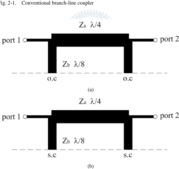
Z
aθ
aZ
b, θ
bport 1
port 2
port 3
port 4
Fig. 2-1. Conventional branch-line coupler
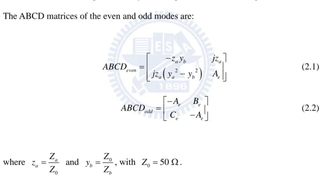
(a)
(b)
Fig. 2-2. Even/odd mode analysis of the circuit in Fig. 2-1. (a) Even mode (b) Odd mode
7
Fig. 2-1 shows the layout of conventional branch-line coupler. The reference impedances for the four ports are 50 ohm. All the sections are quarter-wavelength at the central frequency with characteristic impedances Za and Zb. Signal propagates
along with main line to port 2 (through), and part of signal further continues along with the branch to port 3 (coupling). Port 4 is isolated since the phase difference between two channels is 180 degrees, and then the deconstructive interference occurs. The control of coupling level subject to characteristic impedance of the branch will be demonstrated.
Even/odd mode analysis of the circuit is used to derive the S parameters. The circuits reduced with respect to the symmetric plane are shown in Fig. 2-2 (a) and (b). The ABCD matrices of the even and odd modes are:
(
2 2)
a b a even a a b e z y jz ABCD jz y y A − = − (2.1) e e odd e e A B ABCD C A − = − (2.2) where 0 a a Z z Z = and 0 b b Z y Z = , with Z0 =50 Ω .The conversion between S parameters and ABCD parameters can be written as:
2 11 o e S =Γ +Γ (2.3a) 2 21 o e S =τ +τ (2.3b) 2 31 o e S =τ −τ (2.3c) 2 41 o e S =Γ −Γ (2.3d)
8 where o e o e D C B A D C B A / / − − + − − + = Γ and o e o e D C B A / / 2 − − + = τ . When input is excited at port 1, for instance, S11 = S41 = 0 at the design frequency should be enforced.
Based on these conditions, the S matrix for a branch-line coupler can be derived as follows:
[ ]
0 1 0 0 0 1 1 0 0 0 1 0 1 1 2 + − = b b b b b jz jz jz jz z S (2.4)The diagonal terms in (2.4) vanish for input matching at central frequency, and S41 = S14 = S23 = S32 = 0 for isolation purpose. The ratio jzb
S S
= 31
21 stands for power
division zb2:1 and the phase of through port leading over coupling port. Typically, the fractional bandwidth is about 15% ~ 20%. The circuit size is
16
2
λ .
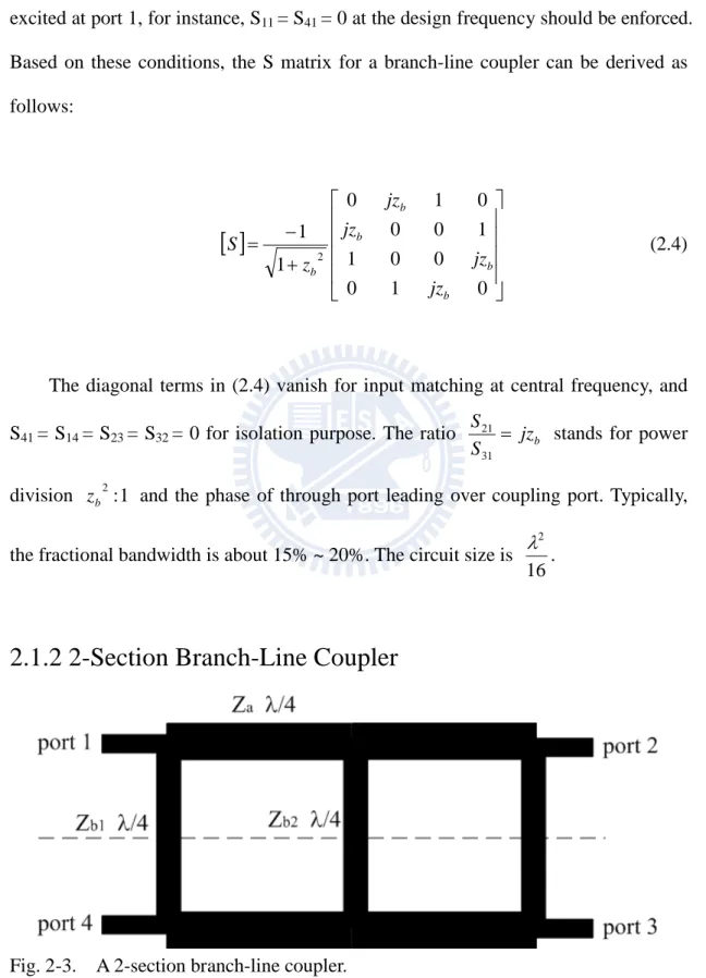
2.1.2 2-Section Branch-Line Coupler
9
Multi-section branch-line coupler can be used to enhance the fractional bandwidth. Fig. 2-3 shows the 2-section branch-line coupler. The analysis procedure is the same as one in previous section. Herein, the design formulas are listed as follows for reference:
2 31 2 2 1 B B y c S y = = − (2.5) 1 0 2 1 1 B c Z Z c = − − (2.6) 2 2 0 A B z Z Z c = (2.7)
where Z0 is the reference impedance, z for normalized impedance and c is coupling. A
Note that z typically ranges between 0.6 and 3 if ZA 0 = 50 ohm. The circuit size is
about 8
2
λ
at the design frequency. It is worth noting that the 2-section branch-line coupler possesses a fractional bandwidth about 30%.
10
2.2 3-Section Branch-Line Coupler
2.2.1 Even/Odd Mode Analysis
Fig. 2-4. A 3-section branch-line coupler with characteristic impedance Za for main
line and Zb1 and Zb2 for branch lines.
11
(b)
(c)
(d)
Fig. 2-5. Even/odd mode analysis for the bisymmetric circuit in Fig. 2-4. (a) Even-even mode (b) Even-odd mode (c) Odd-even mode (d) Odd-odd mode
12
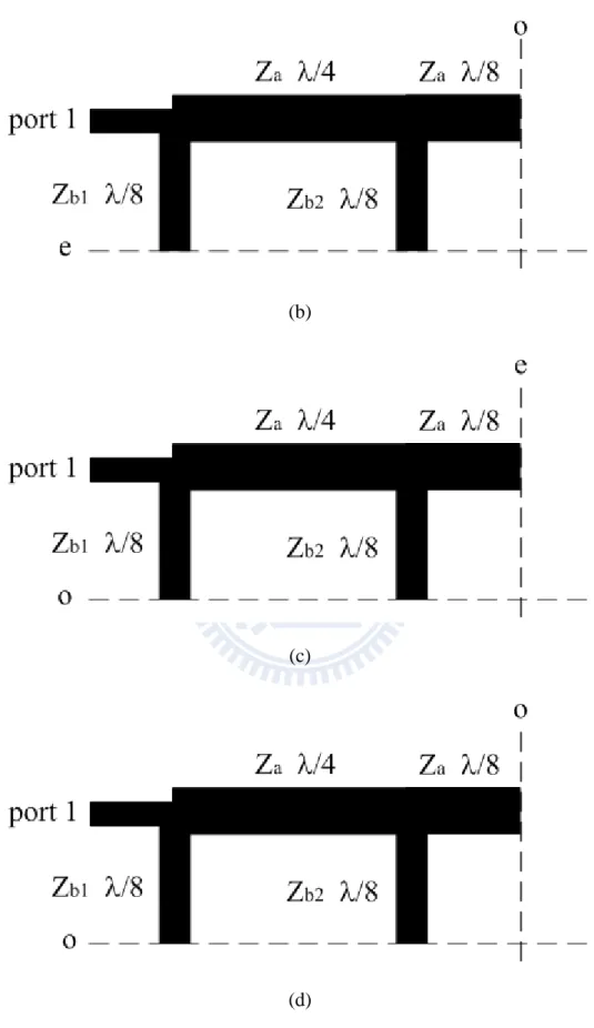
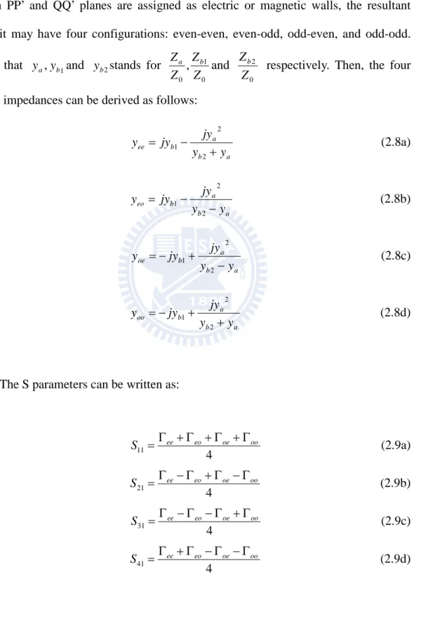
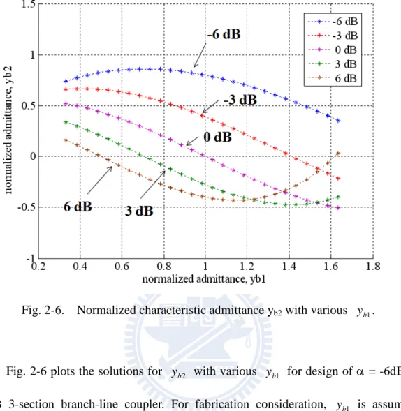
Fig. 2-4 shows layout of a 3-section branch-line coupler. In analysis, the PP’ and
QQ’ planes can be assigned as either an electric or a magnetic wall. Fig. 2-5 (a)
through (d) shows the reduced equivalent circuit of 3-section branch-line coupler when PP’ and QQ’ planes are assigned as electric or magnetic walls, the resultant circuit may have four configurations: even-even, even-odd, odd-even, and odd-odd. Note that ya,yb1and y stands for b2
0 1 0 , Z Z Z Za b and 0 2 Z Zb
respectively. Then, the four input impedances can be derived as follows:
a b a b ee y y jy jy y + − = 2 2 1 (2.8a) a b a b eo y y jy jy y − − = 2 2 1 (2.8b) a b a b oe y y jy jy y − + − = 2 2 1 (2.8c) a b a b oo y y jy jy y + + − = 2 2 1 (2.8d)
The S parameters can be written as:
11 4 ee eo oe oo S =Γ + Γ + Γ + Γ (2.9a) 21 4 ee eo oe oo S =Γ − Γ + Γ − Γ (2.9b) 31 4 ee eo oe oo S = Γ − Γ − Γ + Γ (2.9c) 41 4 ee eo oe oo S =Γ + Γ − Γ − Γ (2.9d)
13 where 1 1 ij ij ij y y − Γ =
+ , the subscripts i and j stand for either e or o.
Based on the input matching and isolation conditions, S11 = S41 = 0, we have:
eo ee =−Γ Γ (2.10a) oo oe =−Γ Γ (2.10b)
For simplicity, the imaginary number j is extracted from y , i.e.ij yee = ja,
jb
yee = , yee = jc and yee = jd. Equating the real part and imaginary part in (2.10a) and (2.10b), we obtain 1− ba2 2 =0 and
(
a+b)(
ab+1)
=0. In addition, c and dhave the same relation as a and b. The conditions in (2.9) can be replaced with the following conditions for input admittances:1 − = ab (2.11a) 1 − = cd (2.11b)
In order to specify arbitrary power divisionα2 :1 , jα S
S
= 31
21 builds up the
relationship between a and c as:
α − = − + a c ac 1 (2.12)
Substituting a, b, c and d into (2.11a) and (2.11b), one can observe that both equations give the same result:
14 0 2 1 2 2 2 2 1 2 2 2 1 = − − + + a b b b a a b y y y y y y y (2.13)
Using (2.12), (2.13) can be reduced into a result that y is in terms of a2 y andb1 y : b2
(
)
(
1 2)
1 2 2 2 1 1 b b b b a y y y y y + − − = α α (2.14)Substituting (2.14) into (2.13), y can be expressed in terms of 2 y : b1
(
)
(
)
(
)
2 1 1 2 1 2 1 1 2 1 α α α + − − − = b b b b y y y y (2.15)Note that y is one degree of freedom to be determined for desired fractional b1
15
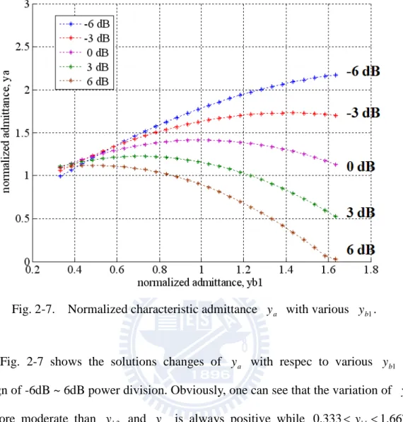
Fig. 2-6. Normalized characteristic admittance yb2 with various y . b1
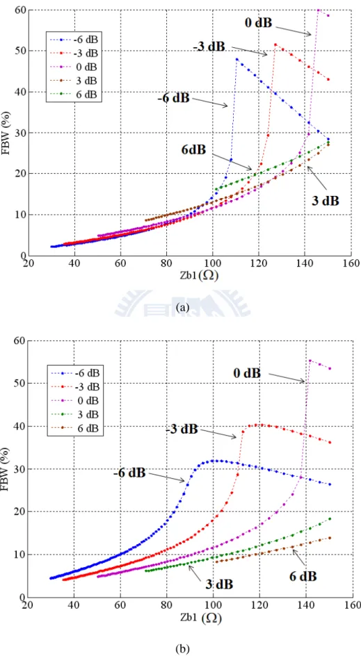
Fig. 2-6 plots the solutions for y with various b2 y for design of α = -6dB ~ b1
6dB 3-section branch-line coupler. For fabrication consideration, y is assumed b1
from 0.333 to 1.667, i.e., 150 ohm and 30 ohm for Z0 = 50Ω. It shows that the feasible region of y decreases as the power division is increased because b2 y b2
must be a positive number larger than 0.333. For instance, for α = 6dB power division design, y is only 0.163, or b2 Zb2 =306.7ohm, whileyb1=0.333. It also implies that
if the more power transmitted to the through port, the higher impedance the branch line has.
16
Fig. 2-7. Normalized characteristic admittance y with various a y . b1
Fig. 2-7 shows the solutions changes of y with respec to various a y to b1
design of -6dB ~ 6dB power division. Obviously, one can see that the variation of y a
is more moderate than y and b2 y is always positive while a 0.333<yb1 <1.667. Besides, for 6dB and -6dB design, the slope of y with respect to a y is positive b1
17
(a)
(b)
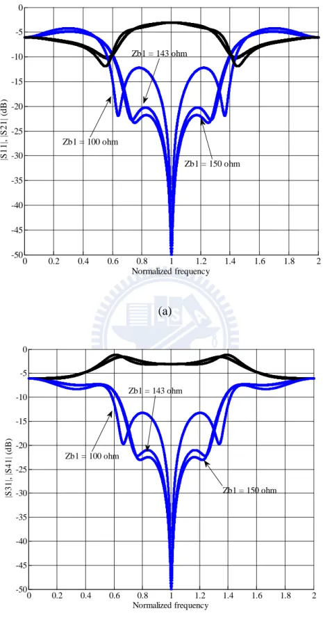
Fig. 2-8. The variation of -20dB fractional bandwidth with variousZ . (a) Sb1 11 (b)
18 0 0.2 0.4 0.6 0.8 1 1.2 1.4 1.6 1.8 2 -50 -45 -40 -35 -30 -25 -20 -15 -10 -5 0 Normalized frequency |S 11| , | S 21| ( dB ) Zb1 = 143 ohm Zb1 = 150 ohm Zb1 = 100 ohm (a) 0 0.2 0.4 0.6 0.8 1 1.2 1.4 1.6 1.8 2 -50 -45 -40 -35 -30 -25 -20 -15 -10 -5 0 Normalized frequency |S 31| , | S 41| ( dB ) Zb1 = 150 ohm Zb1 = 100 ohm Zb1 = 143 ohm (b)
Fig. 2-9 Illustrations for the discontinuity points of the fractional bandwidth prediction. (a) |S11| and |S21| (b) |S31| and |S41|
19
Fig. 2-8 (a) and (b) plot the fractional bandwidth of a 3-section branch-line coupler with various Z for power division of -6 dB to 6 dB. The fractional b1
bandwidths are defined as the frequency band in which the magnitude of the
S-parameter is -20dB. One can see that the bandwidth increases while Z is b1
increased. Note that there is one discontinuity point, for instance, the maximum fractional bandwidth of S11 for 0dB design occurs whenZ is approximately 143 ohm. b1
Investigating the frequency response shown in Fig. 2-9, the bandwidth is located in a narrow window when Z is smaller than 143 ohm, and the bandwidth suddenly b1
becomes maximum because the two local maxima are lower than -20 dB defined as the fractional bandwidth. Interestingly, the bandwidth again decreases when Z is b1
larger than that point. After simulating some solutions near the corner, one can see that the two local maximums vanish gradually and simultaneously the bandwidth becomes narrower. The desired wideband branch-line coupler with specific fractional bandwidth can be designed according to this graph. Table 2-1 compares the maximal fractional bandwidths with various power divisions.
Table 2-1
Summary Data of the Maximal Fractional Bandwidth for |S11| and |S41|
Power division *FBW of |S11| (Zb1) *FBW of |S41| (Zb1) -6 dB 48.56% (109.1 Ω) 31.89% (101.4 Ω) -3 dB 52.22% (125.5 Ω) 40.33% (118.1 Ω) 0 dB 60.67% (143.5 Ω) 55.78% (139.5 Ω) 3 dB 27.11% (150.0 Ω) 18.33% (150.0 Ω) 6 dB 27.78% (150.0 Ω) 14.0% (150.0 Ω) * the FBWs of |S11| and |S41| are in reference of -20 dB.
20
2.2.2 Simulation
Herein, only simulations are demonstrated to verify the idea because the miniaturized circuits are focused in this thesis and will be presented in next chapter. Two circuits are simulated to confirm the formulation by the software package IE3D [22]. The substrate has dielectric constant εr = 2.2 and thickness h = 0.508 mm. One circuit demonstrated is specified for -3 dB power division and the other for 3 dB power division, both with maximal fractional bandwidth of |S41|. The operating
frequency is 1 GHz.
Fig. 2-10 shows the 3-section branch-line coupler with -3 dB power division. In Fig. 2-8 (b), the impedances of Z , b1 Zb2, and Z are 125.12 Ω, 75.0169 Ω , and a
43.9481 Ω, respectively. The circuit size is 163.5 mm×59.03 mm. Fig. 2-11 (a) plots the magnitude responses of the S-parameters when the signal is excited at port 1, the simulation data at fo show that |S11| = –49.18 dB, |S21| = –5.19 dB, |S31| = -2.24 dB and
|S41| = –49.18 dB. The bandwidths in reference of |S11| < -20 dB and |S41| < -20 dB are
53.7% and 40%, respectively. The relative phase difference between S21 and S31 is
21 1.852 mm 0.798 mm 0.244 mm Port 4 Port 3 Port 2 Port 1 59.03 mm 163.5 mm
Fig. 2-10. Physical layout for 3-section branch-line coupler with -3dB power division and maximum fractional bandwidth
S31 S21 41 31 0 -10 -20 -30 -40 -50 2 1.6 1.2 0.8 0.4 0 Simulation 11 |S | , |
S
| , |S
| , |S
| (dB) Frequency (GHz) 21 0.2 0.6 1 1.4 1.8 S11 S41 (a)22
1
Frequency (GHz)
2
0
90
135
45
S
2 1S
3 1-(degr
ee
)
Simulation
(b)Fig. 2-11. Simulation for 3-section branch-line coupler with -3dB power division and maximal fractional bandwidth (a) Magnitude response (b) Relative phase response
Fig. 2-12 shows the 3-section branch-line coupler with 3 dB power division. In Fig. 2-8 (b), the impedances of Z , b1 Zb2, and Z are 150 Ω, 147 Ω, and 45.02 a
Ω, respectively. The circuit size is 163.47 mm×59.37 mm. Fig. 2-13 (a) plots the magnitude responses of the S-parameters when the signal is excited into port 1, the simulation data at fo show that |S11| = –41.69 dB, |S21| = –2.09 dB, |S31| = -5.22 dB and
|S41| = –39.86 dB. The bandwidths in reference of |S11| < -20 dB and |S41| < -20 dB are
28.6% and 19.7%, respectively. The relative phase difference between S21 and S31 is
89.490 in Fig. 2-13 (b). One can observe that the simulation results agree very well with the prediction.
23 0.147 mm 1.82 mm 0.157 mm 59.37 mm 163.47 mm Port 4 Port 3 Port 2 Port 1
Fig. 2-12. The physical layout for 3-section branch-line coupler with 3 dB power division and maximum fractional bandwidth
S41 S11 S31 S21 41 31 0 -10 -20 -30 -40 -50 2 1.6 1.2 0.8 0.4 0 Simulation 11 |S | , |
S
|, |S
|, |S
| (dB) Frequency (GHz) 21 0.2 0.6 1 1.4 1.8 (a)24
1
Frequency (GHz)
2
0
90
135
45
S
2 1S
3 1-(degr
ee
)
Simulation
(b)Fig. 2-13. Simulation for 3-section branch-line coupler with 3 dB power division and maximum fractional bandwidth (a) magnitude (b) phase difference
Based on the principle of branch-line coupler, an extension to have a wide-band branch-line coupler with arbitrary power division and specified fractional bandwidth is performed. Formulation for analyzing the circuit is derived and solution curves are provided. Two circuits are designed and simulated to validate the idea. Good simulation results agree with the design equations and prediction on fractional bandwidth.
Yet, for applications with low operating frequencies, the circuit size implemented by transmission lines is a vital problem due to the miniaturized design trend in modern RF system. Thus, in the next chapter, the miniaturization for a 3-section branch-line coupler is under study.
25
Chapter 3
Miniaturized 3-Section Branch-Line Coupler by
Lumped Distributed - and Lumped Elements
Conventional directional couplers are realized with the use of transmission lines of different types. In MIC, microstrip lines are the most popular transmission line. At frequencies below 20 GHz distributed components occupy large areas and create dimensional problems in MMIC's. Lumped elements are very attractive in applications where size reduction is important. It is known that, at a single frequency, the symmetrical π- or T- LC section is equivalent to the transmission line section with the appropriate characteristic impedance and electrical length. Consequently, the lines which compose a coupler can be partially or completely replaced by lumped sections.
In this chapter, miniaturized 3-section branch-line coupler is implemented by replacing the transmission lines with equivalent circuit models which composes lumped elements such as capacitors and inductors. First, analysis on equivalent circuit models is presented. Then, using these equivalent circuit models, size reduction can be achieved for a 3-section branch-line coupler with good performance.
26
(a)
(b)
Fig. 3-1. Equivalent circuit models for one section of transmission line with arbitrary electrical length θ and characteristic impedance Z0. (a) π model. (b) T model.
27
Fig. 3-1 shows two equivalent circuit models for a section of transmission line with arbitrary electrical length θ and characteristic impedance Z0. For equivalence, the
ABCD matrices of a transmission line and π network should be identical:
0 0 cos sin sin cos TL jZ ABCD jY θ θ θ θ = 2 , 3 1 2 3 3 1 2 1 1 2 3 3 1 1 1 0 1 0 1 1 0 1 1 1 1 lumped Y ABCD Y Y Y Y Y Y Y Y Y Y Y Y π = + = + + +
One can see that due to symmetry of a transmission line section, Y1 and Y2 must be
the same such that the degrees of freedom reduce from 3 to 2. Take the π model as an example, the network has a low-pass function if Y1 and Y3 are shunt capacitors with a
series inductor Y2. After some mathematical manipulations, the values of capacitance
and the inductance can be derived as follows:
0sin L Z ω = θ 0 1 tan 2 C Z θ ω =
Similarly, the network with the high-pass characteristic has the following capacitance and inductance:
0cot
2
L Z θ
28 0 1 sin C Z ω θ =
Note that the capacitance and inductance for the π model with low-pass characteristic are exactly the inverse of the inductance and capacitance for the π model with high-pass characteristic, respectively.
For T models, all capacitances and inductances can be derived with the same approach instead of replacing with the ABCD matrix of T model:
1 1 2 1 2 3 3 , 2 3 3 1 1 1 lumped T Z Z Z Z Z Z Z ABCD Z Z Z + + + = +
Table 3-1 lists the formula for equivalent circuit models with various electrical lengths 300, 450 and 900. For instance, assuming operating frequency is at 1 GHz and Z0 = 50 Ω, the values of capacitances and inductance are calculated for reference.
Note that the sign + stands for equivalent models with low-pass characteristic and the sign − for equivalent models with high-pass characteristic.
29
Table 3-1
Examples of Equivalent Circuit Models with Various Electrical Lengths f0@1 GHz, Z0 = 50 ohm formulation 300 450 900 π+ model ωL=Z0sinθ L (nH) 3.979 5.627 7.958 0 1 tan 2 C Z θ ω = C (pF) 0.853 1.318 3.183 π − model 0cot 2 L Z θ ω = L (nH) 29.699 19.212 7.958 0 1 sin C Z ω θ = C (pF) 6.366 4.502 3.183 T+ model 0tan 2 L Z θ ω = L (nH) 2.132 3.296 7.958 0 sin C Z θ ω = C (pF) 1.592 2.251 3.183 T−model 0 sin Z L ω θ = L (nH) 15.915 11.254 7.958 0 1 cot 2 C Z θ ω = C (pF) 11.879 7.685 3.183 1 , 2 , 3st nd rd rd nd st 1 , 2 , 3 HP equi. (d eg re e) 180 120 60 0 -60 -120 -180 21 S 1.8 1.6 1.4 1.2 1 0.8 0.6 0.4 Ideal TL LP equi. 2 0.2 0 Frequency (GHz)
Fig. 3-2. Phase response of S21 for equivalent circuit models with θ = 300, 450, and
30
Fig. 3-2 plots the phases of S21 for π models with 1st-, 2nd- and 3rd order models
equivalent to one transmission line of 900. One can see that higher order equivalence gives a better approximation. Interestingly, 2nd order model improves the performance much better than the 1st-order one, but the 3rd-order model brings comparatively slight improvement on 2nd-order model. For instance, for a conventional branch-line coupler with 0 dB power division, Fig. 3-3 plots the frequency responses with multi-section equivalent circuit models. The circuit implemented by transmission lines has the FBW 10.5% and the others with 8.12%, 9.45% and 9.95% for 1st-order one to 3rd order, respectively. One can conclude that the 2nd order equivalence is slightly not good as the 3rd-order one, but for lower frequency application, 2nd order model is adequate to approximate a transmission line. Later, the 2nd order model is adopted in consideration of fabrication complexity. Note that the same characteristics described for π models appear in the T models.
0 -10 -20 -30 -40 -50 2 1.6 1.2 0.8 0.4 0 S11 S21 11 |S | , |
S
| (dB) Frequency (GHz) 21 0.2 0.6 1 1.4 1.8 -20 dB 1 , 2 , 3st nd rd (a)31 0 -10 -20 -30 -40 -50 2 1.6 1.2 0.8 0.4 0 S41 S31 31 |S | , |
S
| (dB) Frequency (GHz) 41 0.2 0.6 1 1.4 1.8 -20 dB st nd rd 1 , 2 , 3 (b)Fig. 3-3. Variations of frequency responses with 1st order, 2nd order and 3rd order equivalence. (a) |S11| and |S21| (b) |S31| and |S41|
3.2 Miniaturization by Lumped Distributed Elements
One 3-section branch-line coupler designed at 1 GHz with -3 dB power division and optimal fractional bandwidth is fabricated and measured for demonstration. Fig. 3-4 (a) and (b) shows the layout. The substrate has a relative dielectric constant εr = 2.2 and thickness h = 0.508 mm. The 2-section T network equivalent circuit models for a transmission line section of electrical length +900 and characteristic impedances of 125.12 Ω, 75.0169 Ω , and 43.9481 Ω are used. The circuit is simulated and optimized by the software package ADS [23].
Table 3-2 lists the values used in theory and optimization. The surface mount devices (SMDs) of 0805 are employed. For SMDs, there are some typical values for capacitors and inductors, thus optimization is subject to available values. Note that the
32
shunt capacitors of outer-side branch lines are replaced by open stubs of 50 ohm with appropriate electrical lengths. Using the shunt open stubs brings two advantages: one is controllable variance of transmission line during fabrication with low complexity; the other is design flexibility due to limited lumped element values. In view of
physics, a wider line width corresponds to a larger capacitance. Yet, the coupling
effect between the open stubs occurs when the lines are tightly close coupled. Typically, there is a three-time distance reserved between two transmission lines in case of coupling.
33 1 mm 1.3 mm 0.608 mm 1.56 mm 1.56 mm 5.80 mm 21.99 mm (b)
Fig. 3-4. (a) Layout of 3-section branch-line coupler with -3 dB power division in ADS (Circuit 1) (b) geometric parameters of the quarter circuit.
.
Table 3-2
Summary Data of the Lumped/Distributed Element Values Theory Optimal Lb1 (nH) 8.3802 Lb1 (nH) 10
Lb2 (nH) 4.9471 Lb2 (nH) 4.7
La (nH) 2.9162 La (nH) 3.3
Cb1 (pF) 0.8853 Open stub 50ohm, 5.80
Cb2 (pF) 1.4997 Cb2 (pF) 1.0
34
Two of the four ports of the coupler circuit are connected to a HP8720ES network analyzer using coaxial cables and the other two ports are terminated in 50 ohm resistances, to measure the circuit. The conventional short-open-load-through (SOLT) calibration method is applied to eliminate the effects of the cables. Fig. 3-5 shows the simulated and measured results. Fig. 3-5 (a) and (b) plot |S11|, |S21|, |S31|, and
|S41| responses. Obviously, there is discrepancy that the designed band drifts toward
lower frequency caused by the practical inductances of the surface mount inductors with certain variation. At the operating frequency, |S11| and |S41| are below -25 dB,
while |S21| and |S31| are -6.86 dB and -2.36 dB; both one lower than the theoretical
results. This can be ascribed to the non-ideal lumped elements with parasitic resistances. The measurement indicates that the circuit has bandwidths of 33.15% and 28.28% for |S11| and |S41|, respectively, for a reference of -20 dB. Fig. 3-5 (c) shows
the response of relative phase ∠S31-∠S21 which is 96.540 at 1 GHz. This degradation
of the phase difference is due to parasitic inductance and capacitance of chip devices. Fig. 3-6 shows the photograph of the experimental circuit. Table 3-3 shows the summary data of simulation and experiment.
35 0 -10 -20 -30 -40 -50 2 1.6 1.2 0.8 0.4 0 Measurement Simulation 11 |S |, |
S
| (dB) Frequency (GHz) 21 0.2 0.6 1 1.4 1.8 -20 dB (a) 0 -10 -20 -30 -40 -50 2 1.6 1.2 0.8 0.4 0 Measurement Simulation 31 |S | , |S
| (dB) Frequency (GHz) 41 0.2 0.6 1 1.4 1.8 -20 dB (b)36
1
Frequency (GHz)
2
0
90
135
45
S
21S
31-(degree)
Simulation
Measurement
(c)Fig. 3-5 Simulation and measurement of the 3-section branch-line coupler. (a) |S11|
and |S21| (b) |S31| and |S41|. (c) The simulation and measurement of phase difference
between S21 and S31.
37
Table 3-3
Summary Data of the 3-Section Branch-Line Coupler with -3dB Power Division (Circuit 1) Simulation Measurement Operating frequency 1 GHz 1 GHz Return Loss (|S11|) FBW* -66.41 dB 30.3% -40.60 dB 33.15% Through (|S21|) -4.76 dB -6.86 dB Coupling (|S31|) -1.77 dB -2.36 dB Isolation (|S41|) FBW -68.17 dB 30.4% -19.56 dB 28.28% 21 31 S S ∠ − ∠ 89.990 96.540 * FBWs are in reference of -20 dB level.
3.3 Miniaturization by Lumped Elements
In this section, open stubs are replaced with chip capacitors to implement a 3-section branch-line coupler designed at 1 GHz with -3 dB power division and optimal fractional bandwidth. Fig. 3-7 shows the layout. Table 3-4 lists the values used in theory and optimization. The circuit is simulated and optimized by the software package ADS [23].
38 (a)
0.8 mm
0.908 mm
0.608 mm
1.3 mm
0.708 mm
(b)Fig. 3-7. (a) Layout of 3-section branch-line coupler with -3 dB power division in ADS (Circuit 2). (b) Geometric parameters of the quarter circuit.
39
Table 3-4
Summary Data of the Lumped Element Values Theory Optimal Lb1 (nH) 8.3802 10 Lb2 (nH) 4.9471 4.7 La (nH) 2.9162 3.3 Cb1 (pF) 0.8853 0.5 Cb2 (pF) 1.4997 1 Ca (pF) 2.5441 2
Fig. 3-8 (a) and (b) plot |S11|, |S21|, |S31|, and |S41| responses. At the operating
frequency, |S11| and |S41| are below -20 dB, while |S21| and |S31| are -7.11 dB and -4.66
dB. The measured |S21| and |S31| are lower than the theoretical data because the
capacitors and inductors have parasitic resistances that cause severe power dissipation. The measurement indicates that the circuit has bandwidths of 35.59% and 26.33% for |S11| and |S41|, respectively, for a reference of –20 dB level. Fig. 3-8 (c) shows the
response of relative phase ∠S31-∠S21 which is 90.570 at 1 GHz. Due to the parasitic
inductance and capacitance of SMDs, the fractional bandwidth is narrower than the simulated results with degradation of the phase difference between S21 and S31. Fig.
3-9 shows the photograph of the experimental circuit. Table 3-5 shows the summary data of simulation and experiment.
40 0 -10 -20 -30 -40 -50 2 1.6 1.2 0.8 0.4 0 Measurement Simulation 11 |S |, |
S
| (dB ) Frequency (GHz) 21 0.2 0.6 1 1.4 1.8 -20 dB (a) 0 -10 -20 -30 -40 -50 2 1.6 1.2 0.8 0.4 0 Measurement Simulation 31 |S | , |S
| (dB) Frequency (GHz) 41 0.2 0.6 1 1.4 1.8 -20 dB (b)41
1
Frequency (GHz)
2
0
90
135
45
S
21S
31-(degree)
Simulation
Measurement
Fig. 3-8. Simulation and measurement of the 3-section branch-line coupler with -3dB power division. (a) |S11| and |S21| (b) |S31| and |S41| (c) The simulation and
measurement of phase difference between S21 and S31
42
Table 3-5
Summary Data of the 3-Section Branch-Line Coupler with -3 dB Power Division (Circuit 2) Simulation Measurement Operating frequency 1 GHz 1 GHz Return Loss (|S11|) FBW* -66.47 dB 42.44% -25.87 dB 35.59% Through (|S21|) -4.77 dB -7.11 dB Coupling (|S31|) -1.76 dB -4.66 dB Isolation (|S41|) FBW -69.44 dB 37.94% -26.05 dB 26.33% 21 31 S S ∠ − ∠ 900 90.570 * FBWs are in reference of -20 dB level.
TL Circuit 1 Circuit 2 1 0.8 0.6 0.4 0.2 0 2 1.6 1.2 0.8 0.4 0 Measurement Simulation 1-P ow er Lo ss Frequency (GHz) 0.2 0.6 1 1.4 1.8
Fig. 3-10. Power loss of 3-section branch-line coupler with transmission lines, lumped distributed elements (Circuit 1), and all lumped elements (Circuit 2).
43
Fig. 3-10 plots the power losses for three fabricated circuits. PL = 1 – |S11|2 –
|S21|2 – |S31|2 – |S41|2 at operating frequency for three circuits are 9.3%, 20.2% and
45.8%, respectively. One can see that the power losses increase extremely while the frequency increases. As expected, the circuit with all lumped elements has a severe power loss due to dissipations caused by non-ideal lumped elements, solder and the via holes. This conclusion can be judged by observing that Circuit 1 has fewer capacitors and via holes than Circuit 2. Table 3-6 compares the detailed data for the three implementation approaches of 3-section branch-line coupler. Obviously, the circuit implemented by microstrip lines has good performances with comparatively low power loss, but costs a large area. The performances of the circuits implemented by lumped- and lumped distributed elements are inferior to the former one, but they can reduce the area greatly.
44
Table 3-6
Summary Data for 3 Types of 3-Section Branch-Line Couplers TL Circuit 1 Circuit 2 Operating frequency 1 GHz 1 GHz 1 GHz Return Loss (|S11|) FBW* -37.01 dB 53.94% -40.60 dB 33.15% -25.87 dB 35.59% Through (|S21|) -5.09 dB -6.86 dB -7.11 dB Coupling (|S31|) -2.24 dB -2.36 dB -4.66 dB Isolation (|S41|) FBW -41.46 dB 39.94% -19.56 dB 28.28% -26.05 dB 26.33% 21 31 S S ∠ − ∠ 89.740 96.540 90.570 Circuit Area (mm2) 9651.41 mm2 (100%) 2800 mm2 (29.11%) 653.34 mm2 (6.76%) Power Loss 0.093 0.202 0.458
45
Chapter 4
Conclusion
Based on the principle of a branch-line coupler, an extended work has been presented in this thesis. Using cascading 3 section branch-line couplers, a wide fractional bandwidth design is reported. For arbitrary power division, the corresponding maximum fractional bandwidths are presented. The design curves also reveal that the more uneven power division, the narrower bandwidth the circuit has. Meanwhile, the large size problem due to utilizing transmission lines with quarter-wavelength can be tackled by replacing the transmission line sections with equivalent circuit models implemented by lumped elements or lumped-distributed elements. Yet, the power loss deteriorates the circuit performance while the amount of lumped elements is increased. The prototype circuits are simulated and fabricated to confirm the ideas. The sizes are reduced to 29.11% and 6.76% for the lumped distributed circuit and the lumped circuit. Also, the power losses are 20.2% and 45.8%, respectively. Measurement results are in good agreement with the simulations.
46
References
[1] J. Reed and G. J. Wheeler, “A method of analysis Of Symmetrical four-port net works,” IRE Trans. Micro wave Theory and Techniques, VOI. MT’T-4, pp. 246–252, October 1956.
[2] R. Levy and L. F. Lind, “Synthesis of symmetrical branch-guide directional couplers,” IEEE Trans. Microwai,e Theory Tech., vol. MTT-10, pp. 80-89, 1968. [3] M. Muracuchi, T. Yukitake, and Y. Naito, “Optimum design of 3-dB branch-line couplers using microstrip lines,” IEEE Trans. Microw. Theory Tech., vol. MTT-31, no. 8, pp. 674–678, Aug. 1983.
[4] T. Hirota, A. Minakaw, and M. Muraguchi, “Reduced-size branch-line and rat-race hybrids for uniplanar MMIC’s,” IEEE Trans. Microwave Theory Tech., vol. MTT-38, no. 3, pp. 270–275, Mar. 1990.
[5] I. Sakagami, M. Haga, and T. Munehiro, “Reduced branch-line coupler using eight two-step stubs,” IEE Proc -Microwaves Antennas Propag vol. 146 , 455–460, Dec. 1999
[6] Y.-H. Chun and J.-S. Hong, “Design of a compact broad-band branchline hybrid,” presented at the IEEE MTT-S Int. Microw. Symp. Dig., Long Beach, CA, Jun. 2005. [7] Y.-H.Chun and J.-S.Hong, “Compact wide-band branch-line hybrids”, IEEE Trans
Microwave Theory Tech vol. 54, NO.2, p.704–709, Feb. 2006
[8] C.-W. Tang and M.-G. Chen, “Synthesizing microstrip branch-line couplers with predetermined compact size and bandwidth,” IEEE Trans. Microw. Theory Tech., vol. 55, pp. 1926-1933, Sep. 2007.
[9] S. S. Liao, P. T. Sun, N. C. Chin, and J. T. Peng, “A novel compact-size branch-line coupler,” IEEE Microw. Wireless Compon. Lett., vol. 15, no. 9, pp. 588–590, Sep. 2005.
47
[10] S. S. Liao and J. T. Peng, “Compact planar microstrip branch-line couplers using the quasi-lumped elements approach with nonsymmetrical and symmetrical T-shaped structure,” IEEE Trans. Microw. Theory Tech., vol. 54, no. 9, pp. 3508–3514, Sep. 2006.
[11] K.W. Eccleston and S. M. Ong, “Compact planar microstripline branchline and rat-race couplers,” IEEE Trans. Microwave Theory Tech., vol. 51, no. 10, pp. 2119–2125, Oct. 2003.
[12] C.T. Lin, C.L. Liao and C.H. Chen, “Finite-ground Coplanar-waveguide Branch-line Couplers,” IEEE Microwave and Wireless Components Letters, Vol. 11, No. 3, March 2001, pp. 127–129.
[13] T. N. Kuo, Y. S. Lin, C. H. Wang, and C. H. Chen, “A compact LTCC branch-line coupler using modified-T equivalent-circuit model for transmission line,”
IEEE Microw. Wireless Compon. Lett., vol. 16, no. 2, pp. 90–92, Feb. 2006.
[14] C.-W. Tang, M.-G. Chen, and C.-H. Tsai, “Miniaturization of Microstrip Branch-Line Coupler with Dual Transmission Lines”, IEEE Microw. Wireless
Compon. Lett., vol. 18, pp. 185-187, Mar. 2008.
[15] C.-W. Wang, T.-G. Ma, and C.-F. Yang, “Miniaturized Branch-Line Coupler with Harmonic Suppression for RFID Applications using Artificial Transmission Lines”, in
IEEE MTT-S Int. Microwave Symp. Dig., Jun. 2007,, pp.29-32.
[16] R. K. Gupta and W. J. Getsinger, “Quasi-lumped element 3- and 4-port networks for MIC and MMIC applications,” in IEEE MTT-S Int. Microwave Symp. Dig., CA, 1984, pp. 409–411.
[17] R. W. Vogel, “Analysis and design of lumped- and lumped-distributed element directional couplers for MIC and MMIC applications,” IEEE Trans. Microwave
Theory Tech., vol. 40, pp. 253–262, Feb. 1992.
48
quadrature hybrids,” in Proc. Asia–Pacific Microwave Conf., 1997, pp. 1141–1144. [19] Y.-C. Chiang and C.-Y. Chen, “Design of a wide-band lumped-element 3-dB quadrature coupler,” IEEE Trans. Microw. Theory Tech., vol. 49, no. 3, pp. 476–479, Mar. 2001.
[20] W. S. Tung, H. H. Wu, and Y. C. Chiang, “Design of microwave wide-band quadrature hybrid using planar transformer coupling method,” IEEE Trans.
Microwave Theory Tech., vol. 51, no. 7, pp. 1852–1856, Jul. 2003.
[21] D. M. Polar, Microwave Engineering, 3rd ed. New York: Wiley, 2005, ch. 7. [22] IE3D simulator, Zeland Software Inc., Jan. 2002.
49