掺鎂氧化鋅材料之激子–聲子交互作用研究
126
0
0
全文
(2) 掺鎂氧化鋅材料之激子–聲子交互作用研究 Influence of phonons on excitonic characteristics in Mg-incorporated ZnO 研 究 生:潘 晴 如. Student:Ching-Ju Pan. 指導教授:謝 文 峰 教 授. Advisor:Dr. Wen-Feng Hsieh. 國 立 交 通 大 學 光 電 工 程 研 究 所 博 士 論 文. A Dissertation Submitted to Department of Photonics and Institute of Electro-Optical Engineering College of Electrical Engineering and Computer Science National Chiao Tung University In Partial Fulfillment of the Requirements for the Degree of Doctor of Philosophy in Electro-Optical Engineering. January 2008 Hsinchu, Taiwan, Republic of China. 中華民國九十七年一月.
(3) 誌 謝. 耶!!耶!!耶!!我終於畢業了~~好感動喔,終於完成求學生涯的最後一個階段。 也即將邁入人生的另一個階段,工作賺錢嫁人去嚕^^。 回想博士班生活的點點 滴滴,所有的一切都還歷歷在目,要感謝的人、感動的事實在不勝枚舉。 首先, 我要非常感謝我的指導老師 謝文峰教授。 老師真的是一位有教無類的好老師, 能發掘每個學生潛藏的長處而將其發揮,不僅耐心的引領我找到研究方向,並且 適當的訓練我在學術研究上建立一套邏輯性的思考模式,所謂一日為師終身為父 丫,老師真的像一個爸爸ㄝ,特別是在天南地北的閒聊中感受最為明顯。 然後 我要感謝口試委員們對論文的指導及建議,使得論文更臻完善。 很開心 周武清 老師見證了我從大學、碩士班到博士班的求學歷程。 再來我要謝謝雷射診測實 驗室那些曾經陪伴我ㄧ起走過這些年的夥伴們: 智章學長給我課業上的幫助,丫 政學長以及吳俊毅學弟在我初踏入這個領域時的引導; 林國峰在物理觀念及數 據分析的無私分享與大力協助以及徐瑋澤學弟在實驗量測方面的幫忙; 而黃同 慶就像一個負責任的大家長,處理實驗室相當多的公務與雜事,感覺有他在實驗 室就有大大的支柱呢,也謝謝他在我博士生涯最難熬的時候給我鼓勵,另外我們 與楊松間許多吃喝玩樂的經驗分享也增添了刻板實驗室生活的色彩; 此外玫丹 、明容及盈璇學妹帶給我的歡樂仍然記憶猶新,妳們真是太好玩了! 當然還有謝 謝對我注入刺激的那些人,讓我更有動力往前邁進,在此祝福大家未來學業順利 萬事順心~ 最後我要感謝我親愛的爸爸媽媽偉大的奉獻與支持,拔拔我要回家陪你啦~~ 當然我也知道天上的媽媽一直默默的守護著我。 感謝一直在我身旁給予我全部 的那個人♥.
(4) 掺鎂氧化鋅材料之激子–聲子交互作用研究. 研究生:潘晴如. 指導教授:謝文峰 教授. 國立交通大學光電工程學系暨研究所 摘要 我們利用熱擴散與溶膠-凝膠法製備氧化鎂鋅合金半導體。 利用拉曼散射與 光激發光實驗研究氧化鎂鋅合金的晶格動力學、組成擾動以及激子相關特性(即 激子與聲子、自由載子或其他激子的交互作用)在掺雜不同鎂成分之下的變化情 形。 我們藉由 x-光繞射與光激發光的光譜概略地估計氧化鎂鋅合金中鎂所取代 鋅的比例。 從室溫光激發光與吸收光譜譜峰的藍位移以及晶格常數的改變,可 以證明鎂離子摻入氧化鋅晶體中而且成功地佔據鋅離子的位置。 一般來說,由於合金引起的組成成分擾動會使得拉曼光譜中各種聲子模態發 生變化,如局部晶格改變引發的振動模態、因擾動而活化的振動模態、聲子頻率 的位移、譜形變寬與不對稱等特性。 因此,我們利用拉曼光譜分析當鎂掺入氧 化鋅奈米結構後,氧化鎂鋅晶格振動模態的變化情形。 除了氧化鋅原有的聲子 模態之外,我們亦觀察到 383 與 510 cm-1兩個異常的聲子模態,據推測可能來自 於鎂相關的振動模。 由於鎂離子與鋅離子在半徑上的差異,鎂的摻入會產生某 些新的晶格缺陷抑或是原有的晶格缺陷因擾動而活化進而出現一些額外的振動 模。. I.
(5) 我們用spatial correlation model探討組成成分的擾動造成拉曼光譜譜形變寬 與不對稱的行為;而這個理論模型的概念是考慮聲子的傳播受到合金位能異動 (alloy potential fluctuations)的侷限與晶粒分布(grain size distribution)的影響。 因 此可藉由分析氧化鎂鋅奈米粉末掺鎂的含量多寡與E2(high)聲子的頻率變化之關 聯性得知。 我們發現隨著鎂含量的增加,合金位能異動造成晶粒相對變小,那 是由於受到氧化鎂對氧化鋅溶解度的限制。 多餘的鎂離子無法取代氧化鋅晶體 中鋅離子的位置因而形成氧化鎂群環繞氧化鎂鋅晶體。 在輻射放光過程中雙激子(biexciton)的產生是束縛兩個激子形成,因此激發 能量與輻射放光的強度之間會有接近於2的一個理想指數關係。 我們在氧化鋅粉 末中觀察到聲學聲子(acoustic phonon)與光學聲子(optical phonon)在雙激子形成 的過程中扮演著不可或缺的角色。 研究發現當溫度低於某個程度,也就是激子 動能低於光學聲子動能時,激子或載子(carriers)冷卻(relaxation or cooling)過程僅 有聲學聲子的放射,此時的指數值是小於1的;然而當溫度提高到使得激子動能接 近於光學聲子最低動能的時候,激子或載子冷卻過程多了光學聲子的參與,此時 的指數值則是接近於理論上的理想值。 最後,我們使用變溫光激發光光譜研究掺雜不同鎂成分的氧化鎂鋅粉末其激 子與縱光學聲子(longitudinal optical phonon)耦合強度的變化。 激子與縱光學聲 子的耦合強度可經由分析激子的能量隨著溫度變化所產生的位移來決定。 除此 之外,觀察到隨著鎂成分的提高激子的束縛能相對增加,其原因可能是激子位能 受到合金引發的組成擾動而產生變化。 激子束縛能的增加是由於激子波爾半徑 (Bohr radius)的減小造成激子極性減弱所致,因而降低了激子與縱光學聲子的耦 合強度。. II.
(6) Influence of phonons on excitonic characteristics in Mg-incorporated ZnO. Student: Ching-Ju Pan. Advisor: Dr. Wen-Feng Hsieh. Department of Photonics & Institute of Electro-Optical Engineering National Chiao Tung University. Abstract MgZnO alloys with various Mg contents were successfully synthesized using thermal diffusion and sol-gel methods.. We investigated on the lattice dynamics,. compositional disorder, and exciton-related characteristics (i.e., interactions between excitons and acoustic phonons, LO phonons, free carriers and other excitons) of the MgxZn1-xO alloy semiconductors which depend critically on the Mg substitution using Raman and photoluminescence spectroscopy. Alloy compositions can be estimated from X-ray diffraction patterns and photoluminescence spectra. The blueshift of near-band-edge emission and excitonic absorption along with the variation of lattice parameters reveal that Mg2+ is incorporated into the ZnO host lattice and substitutes for Zn2+. In ternary semiconductor alloys, the Raman spectra show changes of various phonon modes with compositional disorder, including emergence of local vibration modes and disorder-activated modes, a shift in phonon frequency and changes of the linewidth and asymmetry.. In addition to the host phonons of ZnO, two anomalous. modes around 383 and 510 cm-1 are presumably attributed to the Mg-related vibrational modes.. Due to the differences in the ionic radii of Mg impurity and host III.
(7) ions, the Mg-induced extrinsic or intrinsic lattice defects in either substitutional sites or the interstitial sites would become activated.. As a result, disorder-activated. scattering or local lattice vibration occur in Raman scattering. The broadening in linewidth and asymmetry can be investigated in terms of the modified spatial correlation model based on the finite correlation length of a propagation phonon due to the alloy potential fluctuations and grain size distribution. The microscopic nature of the substitutional disorder is discussed by analyzing the compositional. dependence. submicropowders.. of. the. E2(high). phonon. mode. in. MgxZn1-xO. With increasing Mg concentration, the alloy potential. fluctuations lead to a decrease in the grain size, which is induced by the surplus Mg2+ that could form MgO clusters surrounding the MgZnO crystalline. Moreover, it is well known that efficient exciton relaxation is required for bounding two cooled excitons to form biexciton.. Acoustic and optical phonon. scattering playing key roles in exciton relaxation are responsible for formation of biexcitons at various temperatures. Using ZnO powders, we observed a sublinear dependence on excitation power at low temperature, in which the relaxation process involves only emission of acoustic phonons due to the excitons having kinetic energy lower than those of the optical phonons.. However, the exponent comes near. theoretical value of 2 for participation of optical phonons when the exciton kinetic energy approaches to the energy of the lowest optical phonon. Finally, the coupling between exciton and longitudinal optical (LO) phonon was investigated in use of the temperature-dependent photoluminescence from MgxZn1−xO powders (0 ≤ x ≤ 0.05). The exciton binding energy increases to 73 meV for 5 at. % Mg incorporated powders.. It is suggested that the localization of excitons. originating from the compositional fluctuation takes place in MgxZn1−xO alloys. The IV.
(8) strength of exciton-LO-phonon coupling was deduced from the energy shift of exciton emission with temperature variation.. The increase of the exciton binding energy. results from decrease of the exciton Bohr radius that is responsible for reducing the coupling strength of exciton-LO-phonon as increasing Mg content.. V.
(9) Contents Abstract in Chinese…………………………………………………………………… I Abstract in English ……………..………………………………………………….. III Contents……………………………………………………...………………………VI List of Figures………………………………………………………………………..X List of Tables………………………………………………………….....................XIII. Chapter 1 Introduction…………………………………………………………...….1 1.1 Basic properties of ZnO and general review of MgxZn1-xO materials…………… 1 1.1.1 Basic properties of ZnO……………………………………………………1 1.1.2 General review of Mg1-xZnxO materials……………………………………3 1.2 Motives……………………………………………………………………………6 1.3 Organization of the dissertation...………………………………………………...7 References……………………………………………………………………………..9. Chapter 2 Theoretical background………………………………………..……….13 2.1 Crystal structures and Lattice dynamics......………………………………..…….13 2.1.1 Crystal structures…………...……………………………………..………13 2.1.2. Selection. rules. and. phonon. modes……………………. …………………..15 2.1.3 Polar-optical phonons: Fröhlich interaction………………………………20 2.2 Fundamental optical transitions………………...………………………………..24 2.2.1 General conceptions……………….………………………………..…….24 2.2.2 Exciton-related emission ….……………………………………………...26 VI.
(10) 2.2.2.1 Free excitons and polaritons.………………………………………27 2.2.2.2 Bound excitons………………….…………………………………31 2.2.2.3 Two-electron satellites…………………..…………………………33 2.2.2.4 LO-phonon replicas……….…….…………………………………35 2.2.3 Defect emission…………...………………………………………………36 2.2.4 Biexciton and exciton-exciton scattering…………………………………38 References …………………………………………………………………………...42. Chapter 3 Experimental procedures and characterization techniques.…………44 3.1 Synthesis mechanism ……………………………………………………………44 3.1.1 Vapor-Liquid-Solid (VLS) method.…………..…………………………...44 3.1.2 Sol-gel process……………………..……………………………………..45 3.2 Sample preparation……….………………………………………………………48 3.2.1 ZnMgO nanostructures formed by Mg in-diffused ZnO nanowires…...…48 3.2.2 MgxZn1-xO nanopowders synthesized by varying volume ratio of MgO/ ZnO..….….……………………………………………………………….49 3.2.3 MgxZn1-xO powders synthesized by varying molar ratio of Mg/Zn………49 3.3 Characterization of lattice dynamics …………………….………………………50 3.3.1 X-ray Diffraction …………………………………………………………50 3.3.2 Scanning Electron Microscopy …….…………………………………….50 3.3.3 Raman scattering measurement …….…………………………………….50 3.4 Characterization of optical properties ……..…………….………………………52 3.4.1 Photoluminescence system ……………….………………………………52 3.4.2 Optical absorption system ……….……….………………………………52 References …………………………………………………………………………54. VII.
(11) Chapter 4 Raman study of Mg incorporation in MgZnO alloys……...…………56 4.1 Structural and optical properties of ZnMgO nanostructures formed by Mg in-diffused ZnO nanowires.……..…..……..……………………………………57 4.1.1 Morphology……………………………….………………………………57 4.1.2 Determination of Mg concentration………………………………………59 4.1.3 Raman spectra analysis……..…………….………………………………62 4.2 Raman study of alloy potential fluctuations in MgxZn1-xO submicropowders.......65 4.2.1 Morphology and bandgap modulation…....………………………………66 4.2.2 Raman spectra analysis…………………………...………………………68 4.3 Summary.…………………………………………………………………………73 References …………………………………………………………………………...75. Chapter 5 Acoustic and optical phonon assisted formation of biexcitons.............78 5.1 Morphology and temperature-dependent photoluminescence…...………………79 5.2 Excitation-power-dependent photoluminescence……………………...…………81 5.3 Photoluminescence spectra analysis……………………………...………………83 5.4 Summary…………………………………………………………………………86 References …………………………………………………………………………...87. Chapter 6 Reducing exciton–longitudinal optical phonon coupling with increasing Mg incorporation in MgZnO powders…………………………..……89 6.1 Morphology and temperature-dependent photoluminescence…….……………..90 6.2 Binding energy.......................................................................................................93 6.3 Photoluminescence spectra analysis……………………………………………...95 6.4 Summary…………………………………………………………………………98 References …………………………………………………………………………...99 VIII.
(12) Chapter 7 Conclusion and Prospective…………………………………………...101 7-1 Conclusion……………………………………………………………………..101 7-2 Prospective……………………...………………………………………………104 References…………………………………………………………………………..107. Resume …………………………………………………………………………….109 Publication list……………………………………………………………………..110. IX.
(13) List of Figures Fig. 1-1 The wurtzite structure model of ZnO.………….…………………………….1 Fig. 1-2 Typical room temperature PL spectrum of ZnO.…………….……………….3 Fig. 1-3 Tentative form of the system MgO-ZnO.…………….……………………....5 Fig. 2-1 Schematic representation of a wurtzite ZnO structure…………..………….15 Fig. 2-2 Phonon dispersion curves for ZnO crystal of wurtzite structure.…………...18 Fig. 2-3 Displacement vectors of the phonon modes in ZnO wurtzite structure.…….19 Fig. 2-4 A pair excitation in the scheme of valence and conduction band in the exciton picture for a direct gap semiconductor….......................................................26 Fig. 2-5 The electronic band structure of wurtzite ZnO…………...…………………28 Fig. 2-6 Free excitonic fine structure region of the 10 K PL spectrum for the ZnO single crystal……………..……………………………..…………………..29 Fig. 2-7 Dispersion curves of exciton and exciton polaritons…………..……………31 Fig. 2-8 Bound excitonic region of the 10 K PL spectrum for the ZnO single crystal……………………………………………………………………...32 Fig.2-9 10 K PL spectrum in the TES region of the main bound exciton lines……...34 Fig.2-10 10 K PL spectrum in the region where DAP transition and LO-Phonon replicas are expected to appear……………………………………..……...3 Fig.2-11 Inelastic scattering processes in the intermediate density regime: biexciton decay and inelastic exciton-exciton scattering……………...……………...39 Fig.2-12 PL spectra of a ZnO epilayer for various excitation intensities at 77 K…....40 Fig. 3-1 Vapor-Liquid-Solid method.………………...……………………………...45 Fig.3-2 Schematic of the rotes that one could follow within the scope of sol-gel processing…………………………………………………………………...47 X.
(14) Fig. 3-3 XRD ω-2θ scans geometry………………………………………………….50 Fig. 3-4 The scheme of the Raman system….……………………………………….51 Fig. 3-5 PL detection system….……………………………………………………...52 Fig. 3-6 Optical absorption system….………………………………….....................53 Fig. 4-1 The SEM images of the Mg in-diffused ZnO nanowires.. The inset shows. the original aligned ZnO nanowires………………………………………..58 Fig. 4-2 The Rietveld refinement plot of ZMO nanostructures and ZnO nanowires...59 Fig. 4-3 The normalized room-temperature PL spectra of ZMO nanostructures and ZnO nanowires……………………………………………………………..61 Fig. 4-4 The Raman spectra of ZMO nanostructures and ZnO nanowires…………..62 Fig. 4-5 The SEM image of the 10.9% Mg sample………………………………..…66 Fig. 4-6 Photoluminescence and absorption spectra of MgxZn1-xO alloys for different MgO/ZnO volume ratios..………………………………………….……….67 Fig. 4-7 The calculated Mg content in the MgxZn1-xO submicropowders as a function of the MgO/ZnO volume ratio……………………………………………...68 Fig. 4-8 Micro-Raman spectra of the MgxZn1-xO submicropowders with various Mg contents …………………………………………………………………....69 Fig. 4-9 Experimental and calculated line shapes of the E2(high) band for MgxZn1-xO submicropowders with x = 6%, 11%, and 13%.…….……………...……....71 Fig. 4-10 Linewidth. Δτ. and correlation length Lo of E2(high) phonon as a function of. Mg concentration..........................................................................................72 Fig. 5-1 The SEM image of the ZnO powders………………………..……………...79 Fig. 5-2 Temperature dependence of PL spectra in ZnO powders…………………...80 Fig. 5-3 Dependence of the PL spectra on the excitation power measured at 10 K….81 Fig. 5-4 Dependence of PL spectra on excitation power measured at 80 K………....82. XI.
(15) Fig. 5-5 Integrated emission intensity of biexciton as a function of excitation power under various temperatures.……..…………………………………….…....83 Fig. 5-6 Experimental and calculated exciton energies plotted against inverse temperature.........…………………………………………………………...85 Fig. 6-1 The SEM image of the 5% Mg sample.…………..…………………………90 Fig. 6-2 Temperature dependence of PL spectra in ZnO powders…………………...92 Fig. 6-3 Temperature dependence of PL spectra in Mg0.05Zn0.95O powders………....93 Fig. 6-4 Normalized integrated intensity of ZnO sample as a function of temperature.………………………………………………………………94 Fig. 6-5 Normalized integrated intensity of Mg0.05Zn0.95O sample as a function of temperature…………………………………………………………………94 Fig. 6-6 Diagram of exciton-phonon interaction in the unit cell.………………….…95 Fig. 6-7 Dependence of PL peak energy positions on temperature for the MgxZn1−xO alloys……………………………...…………...………………...…………...96 Fig. 6-8 The coupling strength of the exciton-LO-phonon given as the average ratio λratio = λMgxZn1−xO/λZnO for comparison with the exciton Bohr radius aEB…..97. XII.
(16) List of Tables Table 1-1 Properties of wurtzite ZnO………….………………………………………2 Table 2-1 Phonon mode frequencies of wurtzite ZnO at the center of the Brillouin zone obtained from infrared spectroscopic ellipsometry and Raman scattering measurements in comparison with theoretical predictions……19 Table 4-1 Phonon modes frequencies in our work and tentative assignments of all the peaks…….………………………………………………………………...63 Table 6-1 Summary of the results of the temperature-dependent photoluminescence characterization…………………………………………………………....97. XIII.
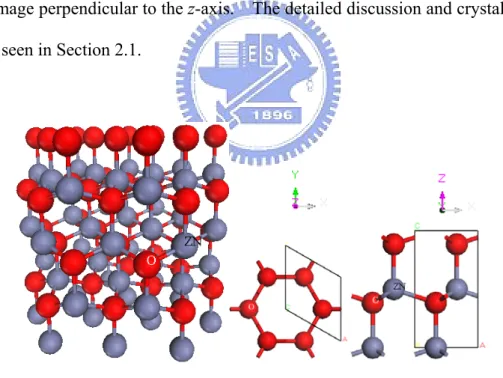
(17) Chapter 1 Introduction. 1.1 Basic properties of ZnO and general review of MgxZn1-xO materials 1.1.1 Basic properties of ZnO The ZnO crystal has wurtzite structure as schematically shown in Fig. 1-1 with lattice constants of a = 3.249 Å and c = 5.207 Å. Zn and O atoms, respectively.. The gray and red spheres denote. The center picture of Fig. 1-1 displayed the top view. image parallel to the z-axis, i.e., c-axis, while the right-most picture displayed the side view image perpendicular to the z-axis. The detailed discussion and crystal structure can be seen in Section 2.1.. Fig. 1-1 The wurtzite structure model of ZnO.. The basic materials parameters of ZnO are shown in Table 1-1. band gap semiconductor with Eg = 3.37 eV at room temperature (RT).. ZnO is a direct The band gap. of ZnO can be tuned via divalent substitution on the cation site to produce heterostructures.. Cd doping will decrease the band gap to as low as 3.0 eV, whereas 1.
(18) Mg doping increase the band gap to as high as 4.0 eV.. Electron doping in nominally. undoped ZnO has been attributed to Zn interstitials, oxygen vacancies, or hydrogen. The intrinsic defect levels that lead to n-type doping lie approximately at around 0.01-0.05 eV below the conduction band. The optical properties of ZnO, studied using photoluminescence (PL), photoconductivity, and absorption reflect the intrinsic direct band gap, a strongly bound exciton state, and gap states arising from point defects.. Shown in Fig. 1.2 is the typical RT PL spectrum.. A strong RT,. near-band-edge (NBE) UV photoluminescence peak at ~ 3.2 eV is attributed to an exciton state, as the exciton binding energy is ~ 60 meV. emission is also observed as a result of defect states.. The detailed optical transitions. of PL spectrum will be further discussed in Section 2.2.. Table 1-1 Properties of wurtzite ZnO. [1]. 2. In addition, visible.
(19) PL Intensity (a.u.) 2.1. 2.4. 2.7. 3.0. 3.3. 3.6. Photon Energy (eV) Fig. 1-2 Typical room temperature PL spectrum of ZnO.. 1.1.2 General review of Mg1-xZnxO materials ZnO is a direct band gap semiconductor with optical properties similar to GaN. Its high band gap energy of 3.37 eV at RT [2] and free-exciton binding energy of 60 meV [3] (much larger than that of GaN ~ 26 meV) along with its larger absorption coefficient compared to GaN make ZnO a promising candidate for the development of short-wavelength photonic devices, such as ultraviolet detectors, light-emitting diodes (LEDs), and laser diodes (LDs).. The large exciton binding energy has enabled. observation of laser action and/or stimulated emission of exciton at temperatures well above RT in ZnO thin films [4-6] and in ZnO/(Mg,Zn)O supperlattices (SLs) [7]. A lower lasing threshold can be expected, if exciton-related recombination is used, rather than recombination of an electron-hole plasma, which is the dominant mechanism of laser action in (In,Ga)N devices.. Therefore, it is expected that a. ZnO-based light emitter should be much brighter than its counterpart of GaN light emitter.. Furthermore, the recent availability of large size high crystalline quality. bulk ZnO can also be considered as an advantage not only for homoepitaxial ZnO. 3.
(20) growth, but also for GaN growth due to its potential as a suitable substrate with similar crystalline properties. ZnO is typically n-type and attempts to fully utilize ZnO-based technologies; p-type doping and band gap engineering are still the remaining issues in modern optoelectronics.. Jingbo et al. [8] proposed that, using the first-principles. band-structure calculations, the p-type dopability of ZnO can be improved by lowering the ionization energy of acceptors in ZnO by codoping acceptors with donor or isovalent atoms (e.g., Mg or Be). Many groups have successfully achieved p-type ZnO by single doping of I or V group elements, such as N [9-15], P [16-19], As [20-23], Li [24], etc., and by codoping of III-N groups, such as Al-N, Ga-N etc [25,26]. ZnO p-n junction LEDs have also been produced by using N-doped p-type ZnO recently, which emit blue or yellow light.[27-29]. However, the dominant. emissions do not come from near-band-edge (NBE) recombination but is related to defects with deep levels. To obtain strong NBE violet emission and even high effective UV laser, it is necessary to prepare LED and LD with active layers of ZnO SL or quantum well (QWs), which need high quality p-type ZnO and p-type ZnO alloy barrier materials. Lately, p-type ZnMgO has been achieved by doped with N, P, Li, and Sb elements.[30-33] Moreover, band gap modulation has played an important role in modern optoelectronics since the emergence of SLs and QWs.. The widely used. semiconductors GaN and GaAs both have their counterparts of AlGaN and AlGaAs with adjustably enlarged band gap to combine with to fabricate various heterostructures so as to realize desired functions.. In recent years, alloying the ZnO. with MgO has been investigated for widening the band gap of ZnO-based structures by adjusting the Mg concentration. MgO (Eg = 7.8 eV) has a NaCl type cubic. 4.
(21) structure with the lattice constant of a = 4.24 Å, while ZnO has a wurtzite structure. According to the phase diagram of ZnO-MgO binary system shown in Fig. 1-3, the thermodynamic solubility limit of MgO in ZnO is less than 4 mol % in the bulk form.[34]. However, ionic radius of Mg2+ (0.57 Å) is similar to that of Zn2+ (0.60 Å),. which may alloy by significant replacement of one another. In spite of a large structural dissimilarity between ZnO and MgO, the successful growth of ternary solid solutions MgxZn1-xO with metastable wurtzite for Mg compositions up to x = 0.45 or with zinc blende crystals for x > 0.5 as demonstrated by Koike et al. [35] and Choopun et al. [36], respectively.. Fig. 1-3 Tentative form of the system MgO-ZnO.. (Mg,Zn)O alloys have been proved feasible to realize the band gap modulation of ZnO.. So MgZnO can be used as barrier layers for carrier confinement.. For. example, Lim et al. [37] demonstrated the operation of the ZnO light-emitting devices emitted 380 nm UV light at room temperature with a turn-on voltage of 3.2 V.. The. intensity of near band edge emission was increased further and greatly suppressed the 5.
(22) deep level emission by using Mg0.1Zn0.9O layers as energy barrier layers to confine the carriers to the high-quality n-type ZnO. ZnO/Mg0.2Zn0.8O coaxial nanorod single quantum well structures were reported by Bae et al. [38], who proposed that the quantum confinement effect would depend on the Mg0.2Zn0.8O barrier layer thickness as well as the ZnO well layer thickness. Additionally, they are also very promising materials for use as active layers in double heterostructures, not only as barrier layers, e.g., Shibata et al. [39] reported high-quality Zn1-xMgxO alloys are very brilliant light emitters, even more brilliant than ZnO, particularly in the high-temperature region. The authors have revealed that the increase in the oscillator strength is mainly due to the increase in the activation energy required for the nonradiative recombination processes.. It is inferred that the localization of excitons originating from the. compositional fluctuation takes place in Zn1-xMgxO alloys.. 347 nm UV. electroluminescence resulted from the NBE emission of MgxZn1-xO was realized on a MgxZn1-xO-based metal-insulator (SiO2)-semiconductor (MIS) structure on a silicon substrate. Therefore, these applications require a full understanding of optical and structural properties of MgZnO materials.. 1.2 Motives Since Raman scattering can yield important information about the nature of the solid on a scale of the order of a few lattice constants, it can be used to study the microscopic nature of structural and/or topological disorder. Raman scattering thus has been widely used to study the local lattice vibration and alloy potential fluctuations of substitutional semiconductor alloys.. Besides, PL measurement is a. suitable tool to determine the crystalline quality and the presence of impurities in the material as well as exciton fine structures. It is imperative to fully characterize the 6.
(23) excitons in ZnO since not only are excitons a sensitive indicator of material quality but also they play an important role in the stimulated emission and gain processes in real device structures.. Especially, the exciton-phonon interaction has significant. influence on the optical properties of alloy semiconductors. To date, little is known about the influence of phonons on optical characteristics in the MgxZn1-xO ternary solid solutions.. A precise knowledge of fundamental. material parameters is essential, in particular, the lattice dynamic properties, exciton-related parameters, and the exciton-phonon interaction as Mg was introduced into the ZnO.. In the dissertation, the MgZnO samples were prepared by the. vapor-phase transport and sol-gel process as described in the experimental procedures of the sample preparation in the later chapter.. We will investigate the interesting. optical features of local lattice structure, Raman vibrational properties, alloy potential fluctuations, and exciton-LO-phonon coupling in use of Raman and PL spectroscopy.. 1.3 Organization of the dissertation This dissertation is organized as follows. Chapter 2 presents a general concept of crystal structures, lattice dynamics, and fundamental optical transitions. Optical transitions in ZnO systems are reviewed in terms of PL features, including exciton-related emissions, defect-related transitions, biexciton and exciton-exciton scattering. In Chapter 3, the synthesis of the MgZnO alloys with different processes is demonstrated.. We also show the brief illustrations of characterization techniques.. In Chapter 4, the band gap modulation of the MgxZn1-xO alloys is discussed. The changes of lattice structure and vibrational properties of ZnO caused by Mg incorporation are also investigated. The Mg-related lattice vibrations and the nature 7.
(24) of the alloy potential fluctuations are demonstrated by Raman study.. Chapter 5. elucidates a detailed discussion on the formation of biexciton assisted by acoustic and optical phonon scatterings. In Chapter 6, we discuss the increase of exciton binding energy may result from the decrease of exciton Bohr radius making the exciton less polar thereby reducing the coupling to LO phonons.. Reducing exciton-LO phonon. coupling with increasing Mg substitution in MgZnO powders will be explained. In the final Chapter 7, we conclude the studies on the MgZnO alloys and propose the several topics of the future work.. 8.
(25) References [1] D. P. Norton, Y. W. Heo, M. P. Ivill, K. Ip, S. J. Pearton, M. F. Chisholm, and T. Steiner, Materials Today 34 (2004). [2] Y. F. Chen, D. M. Bagnall, H. Koh, K. Park, K. Hiraga, Z. Zhu, and T. Yao, J. Appl. Phys. 84, 3912 (1998). [3] K. Hümmer, Phys. Status Solidi B 56, 249 (1943). [4] P. Yu, Z. K. Tang, G. K. L. Wong, M. Kawasaki, A. Ohtomo, H. Koinuma, and Y. Segawa, in Proccedings of the 23rd International Conference on Physics of Semiconductors, Berlin, edited by M. Scheffler and R. Zimmermann (World Scientific, Singapore, 1996), Vol. 2, p. 1453. [5] P. Yu, Z. K. Tang, G. K. L. Wong, M. Kawasaki, A. Ohtomo, H. Koinuma, and Y. Segawa, Solid State Commun. 103, 459 (1997). [6] D. M. Bagnall, Y. F. Chen, Z. Zhu, T. Yao, S. Koyama, M. Y. Shen, and T. Goto, Appl. Phys. Lett. 70, 2230 (1997). [7] A. Ohtomo, K. Tamura, M. Kawasaki, T. Makino, Y. Segawa, Z. K. Tang, G. Wong, Y. Matsumoto, and H. Koinuma, Appl. Phys. Lett. 77, 2204 (2000). [8] J. Li, S. H. Wei, S. S. Li, and J. B. Xia, Phys. Rev. B 74, 081201 (2006). [9] A. Tsukazaki, A. Ohtomo, T. Onuma, M. Ohtani, T. Makino, M. Sumiya, K. Ohtani, S. F. Chichibu, S. Fuke, Y. Segawa, H. Ohno, H. Koinuma, and M. Kawasaki, Nat. Mater. 4, 42 (2005). [10] J. M. Bian, X. M. Li, C. Y. Zhang, W. D. Yu, and X. D. Gao, Appl. Phys. Lett. 85, 4070 (2004). [11] D. C. Look, D. C. Reynolds, C. W. Litton, R. L. Jones, D. B. Eason, and G. Cantwell, Appl. Phys. Lett. 81, 1830 (2002). [12] H. W. Liang, Y. M. Lu, D. Z. Shen, Y. C. Liu, J. F. Yan, C. X. Shan, B. H. Liu, Z. Z. Zhang, J. Y. Zhang, and X. W. Fan, Phys. Status Solidi A 202, 1060 9.
(26) (2005). [13] J. G. Lu, Z. Z. Ye, F. Zhuge, Y. J. Zeng, B. H. Zhao, and L. P. Zhu, Appl. Phys. Lett. 85, 3134 (2004). [14] E. Kamińska, A. Piotrowska, J. Kossut, R. Butkutė, W. Dobrowolski, R. Łukasiewicz, A. Barcz, R. Jakiela, E. Dynowska, E. Przeździecka, M. Aleszkiewicz, P. Wojnar, and E. Kowalczyk, Phys. Status Solidi C 2, 1119 (2005). [15] X. Li, Y. Yan, T. A. Gessert, C. L. Perkins, D. Young, C. DeHart, M. Young, and T. J. Coutts, J. Vac. Sci. Technol. A 21, 1342 (2003). [16] D. K. Hwang, H. S. Kim, J. H. Lim, J. Y. Oh, J. H. Yang, S. J. Park, K. K. Kim, D. C. Look, and Y. S. Park, Appl. Phys. Lett. 86, 151917 (2005). [17] V. Vaithianathan, B. T. Lee, and S. S. Kim, Phys. Status Solidi A 201, 2837 (2004). [18] K. K. Kim, H. S. Kim, D. K. Hwang, J. H. Lim, and S. J. Park, Appl. Phys. Lett. 83, 63 (2003). [19] Z. Q. Chen, A. Kawasuso, Y. Xu, H. Naramoto, X. L. Yuan, T. Sekiguchi, R. Suzuki, and T. Ohdaira, J. Appl. Phys. 97, 013528 (2005). [20] Y. R. Ryu, T. S. Lee, and H. W. White, Appl. Phys. Lett. 83, 87 (2003). [21] D. C. Look, G. M. Renlund, R. H. Burgener II, and J. R. Sizelove, Appl. Phys. Lett. 85, 5269 (2004). [22] V. Vaithianathan, B. T. Lee, and S. S. Kim, Appl. Phys. Lett. 86, 062101(2005). [23] T. S. Jeong, M. S. Han, C. J. Youn, and Y. S. Park, J. Appl. Phys. 96, 175 (2004). [24] J. G. Lu, Y. Z. Zhang, Z. Z. Ye, L. P. Zhu, L. Wang, and B. H. Zhao, Appl. Phys. Lett. 88, 222114 (2006). [25] A. V. Singh, R. M. Mehra, A. Wakahara, and A. Yoshida, J. Appl. Phys. 93, 396 10.
(27) (2003). [26] D. C. Park, I. Sakaguchi, N. Ohashi, S. Hishita, and H. Haneda, Appl. Surf. Sci. 203/204, 359 (2003). [27] A. Tsukazaki, T. Onuma, M. Ohtani, T. Makino, M. Sumiya, K. Ohtani, S. F. Chichibu, S. Fuke, Y. Segawa, H. Ohno, H. Koinuma, and M. Kawasaki, Nat. Mater. 4, 42 (2005). [28] S. J. Jiao, Z. Z. Zhang, Y. M. Lu, D. Z. Shen, B. Yao, J. Y. Zhang, B. H. Li, D. X. Zhao, X. W. Fan, and Z. K. Tang, Appl. Phys. Lett. 88, 031911 (2006). [29] W. Liu, S. L. Gu, J. D. Ye, S. M. Zhu, S. M. Liu, X. Zhou, R. Zhang, Y. Hang, and C. L. Zhang, Appl. Phys. Lett. 88, 092101 (2006). [30] Y. M. Ye, Z. Z. Ye, L. L. Chen, B. H. Zhao, and L. P. Zhu, Appl. Surf. Sci. 253, 2345 (2006). [31] Y. W. Heo, Y. W. Kwon, Y. Li, S. J. Pearton, and D. P. Norton, Appl. Phys. Lett. 84, 3474 (2004). [32] P. Wana, N. F. Chen, Z. G. Yin, R. X. D, and Y. M. Bai, Appl. Phys. Lett. 89, 202102 (2004). [33] M. X. Qiu, Z. Z. Ye, H. P. He, Y. Z. Zhang, X.Q. Gu, L. P. Zhu, and B. H. Zhao, Appl. Phys. Lett. 90, 182116 (2007). [34] J. F. Sarver, F. L. Katnack, and F. A. Hummel, J. Electrochem. Soc. 106, 960 (1959). [35] K. Koike, K. Hama, I. Nakashima, G. Takada, K. Ogatha, S. Sasa, M. Inoue, and M. Yano, J. Cryst. Growth 278, 288 (2005). [36] S. Choopun, R. D. Vispute, W. Yang, R. P. Sharma, T. Venkatesan, and H. Shen, Appl. Phys. Lett. 80, 1529 (2002). [37] J. H. Lim, C. K. Kang, K. K. Kim, I. K. Park, D. K. Hwang, and S. J. Park, Adv. Mater. 18, 2720 (2006). 11.
(28) [38] J. Y. Bae, J. Yoo, and G. C. Yi, Appl. Phys. Lett. 89, 173114 (2006). [39] H. Shibata, H. Tampo, K. Matsubara, A. Yamada, K. Sakurai, S. Ishizuka, and S. Niki, and M. Sakai, Appl. Phys. Lett. 90, 124104 (2007).. 12.
(29) Chapter 2 Theoretical background. In this chapter, crystal structures, lattice dynamics, and fundamental optical transitions of ZnO are reviewed. Lattice dynamics corresponding to the selection rules, lattice vibrational properties, and polar-optical phonon scattering mechanism are discussed.. Optical transitions in ZnO have been studied by a variety of. experimental techniques such as optical absorption, transmission, reflection, photoluminescence (PL), and cathodoluminescence spectroscopies, etc.. In Section. 2.2, we reviewed some fundamental issues related to the optical properties of ZnO single crystal by PL measurement. After understanding the excitonic fine structures associated with either intrinsic or extrinsic transitions, we would describe the various sharp emission peaks observed in PL spectra more specifically for Chapter 5 and 6.. 2.1 Crystal structures and Lattice dynamics 2.1.1 Crystal structures [1] ZnO is a II-VI compound semiconductor whose ionicity resides at the borderline between covalent and ionic semiconductor. The crystal structures shared by ZnO are wurtzite, zinc blende, and rocksalt. At ambient conditions, the thermodynamically stable phase is wurtzite. The wurtzite structure has a hexagonal unit cell with two lattice parameters, a and c, and belongs to the space group of C6v4 or P63mc. A schematic representation of the wurtzitic ZnO structure is revealed in Fig. 2-1. The structure is composed of two interpenetrating hexagonal-close-packed (hcp) sublattices, each of which consists of one type of atom displaced with respect to each other along the threefold c-axis by the amount of u in fractional coordinates (the u. 13.
(30) parameter is defined as the length of the bond parallel to the c axis, in units of c). Each sublattice includes four atoms per unit cell and every atom of one kind (group-II atom) is surrounded by four atoms of the other kind (group VI), or vice versa, which are coordinated at the edges of a tetrahedron. In a real ZnO crystal, the wurtzite structure deviates from the ideal arrangement, by changing the c/a ratio or the u value. It should be pointed out that a strong correlation exists between the c/a ratio and the u parameter in that when the c/a ratio decreases, the u parameter increases in such a way that those four tetrahedral distances remain nearly constant through a distortion of tetrahedral angles due to long-range polar interactions. The lattice parameters of any crystalline material are commonly and most accurately measured by high resolution x-ray diffraction. Several groups reported the measured and calculated lattice parameters, c/a ratio, and u parameter for ZnO crystallized wurtzite structures.. The lattice constants mostly range from 3.2475 to. 3.2501 Å for the a parameter and from 5.2042 to 5.2075 Å for the c parameter.. The. c/a ratio and u parameter vary in a slightly wider range, from 1.593 to 1.6035 and from 0.383 to 0.3856, respectively.. The deviation from that of the ideal wurtzite. crystal is probably due to lattice stability and ionicity.. It has been reported that free. charge is the dominant factor responsible for expanding the lattice proportional to the deformation potential of the conduction-band minimum and inversely proportional to the carrier density and bulk modulus.. The point defects such as zinc antisites,. oxygen vacancies, and extended defects, such as threading dislocations, also increase the lattice constant, albeit to a lesser extent in the heteroepitaxial layers.. 14.
(31) Fig. 2-1 Schematic representation of a wurtzite ZnO structure having lattice constants a and c; u is the bond length, and α and β are the bond angles. [1]. 2.1.2 Selection rules and phonon modes [2,3] When photons from a laser are scattered from a crystal with emission or absorption of phonons, the energy shifts of the photons are small, but can be measured by interferometric techniques.. Usually, the phonon wave vectors are very small. compared to the size of the Brillouin zone so that the interactions are only with zone center phonon.. Thus, one can have interaction with either the zone center acoustic. phonons or the optical phonons.. The interaction with acoustic phonons is called. Brillouin scattering while the interaction with optical phonons is call Raman scattering.. All of the Raman mode frequencies, intensities, line-shapes, and. line-widths, as well as polarizations can be used to characterize the lattices and impurities.. The intensity gives information on crystallinity.. The line-width. increases when a material is damaged or disordered, because damage or disorder occurs in a material will increase phonon damping rate or relax the rules for momentum conservation in Raman process. The different long-wavelength phonon branches in a given crystal correspond to 15.
(32) different symmetries of vibration of the atoms in the unit cell and are characterized by irreducible representations of the space group of the crystal lattice.. If the. wavelengths of the Raman phonons are assumed to be effectively infinite, then the crystal point group can be used in classifying the phonon symmetries. This infinite wavelength assumption is not valid for Raman-active phonons which are also infrared active, and this type of vibration will be discussed separately in the following section. The selection rules for Raman-active phonons can be determined by standard group-theoretical methods and the calculation is described in some detail by Heine, who based his work on the polarizability derivative theory of Born and Bradburn. The result of this approach is that a phonon can participate in a first-order Raman transition if and only if its irreducible representation is the same as one of the irreducible representations which occur in the reduction of the representation of the polarizability tensor. The irreducible representations by which the components of the polarizability tensor transform are conveniently listed by Herzberg and Wilson et al. for the set of molecular point groups, which includes the 32 crystal point groups. The intensity of the Raman-scattered radiation depends in general on the directions of observation and illumination relative to the principal axes of the crystal. The angular variation of the scattering gives information about the symmetry of the lattice vibration responsible.. The anisotropy of the scattering can be predicted for a. vibration of any given symmetry by standard group-theoretical methods. GaN-, AlN- and InN-based materials are highly stable in the hexagonal wurtzite structure although they can be grown in the zinc blende phase and unintentional phase separation and coexistence may occur. The wurtzite crystal structure belongs to the space group C6v4 and group theory predicts zone-center optical modes are A1, 2B1, E1 B. and 2E2.. The A1 and E1 modes and the two E2 modes are Raman active while the B 16.
(33) modes are silent.. The A and E modes are polar, resulting in a splitting of the LO and. the transverse (TO) modes.. The Raman tensors for the wurtzite structure are as. follows: ⎛a ⎜ ⎜0 ⎜0 ⎝ ⎛0 ⎜ ⎜0 ⎜c ⎝. 0 0⎞ ⎟ a 0⎟ 0 b ⎟⎠. A1 ( z ) mode. 0 c⎞ ⎟ 0 0⎟ 0 0 ⎟⎠ ⎛0 0 0⎞ ⎜ ⎟ ⎜0 0 c⎟ ⎜0 c 0⎟ ⎝ ⎠ 0 0⎞⎛ 0 ⎛f ⎜ ⎟⎜ ⎜ 0 − f 0⎟⎜ − f ⎜ 0 0 0⎟⎜ 0 ⎝ ⎠⎝. E1 ( x) mode. (2.1) E1 ( y ) mode −f 0 0. 0⎞ ⎟ 0⎟ 0 ⎟⎠. E2 mode.. Here x, y or z in brackets after an irreducible representation indicates that the vibration is also infra-red active and has the direction of polarization indicated.. Such. vibrations occur only in piezo-electric crystals (i.e. crystals with no center of inversion symmetry).. In crystals which do have a center of inversion symmetry,. only even-parity vibrations, whose representations have a subscript g, can be Raman active and only odd-parity (subscript u) vibrations can be infrared active. This fact leads to the important complementary nature of infra-red absorption and Raman effect measurements. Directly above each irreducible representation is a matrix which μ gives the non-vanishing components of the Raman tensor, i.e. of αρσ,μ or Rσρ .. The. different elements of the matrices are the nine components of the tensor obtained by allowing both ρ and σ to take on the values x, y and z.. Here x, y, and z are the crystal. principal axes chosen to be identical with the principal axes x1, x2 and x3 defined for all the crystal classes by Nye.. The component μ of the phonon polarization for the. 17.
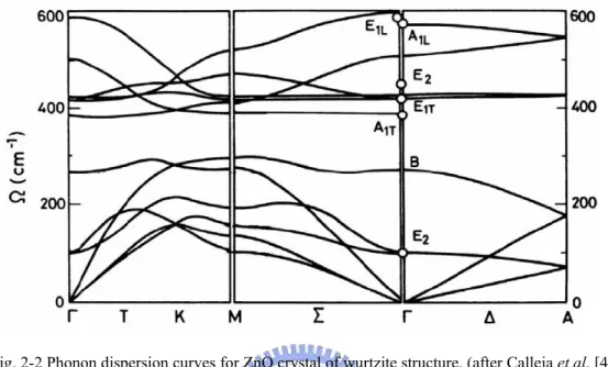
(34) case of infrared-active vibrations is the quantity given in brackets after the irreducible representation symbol.. Fig. 2-2 Phonon dispersion curves for ZnO crystal of wurtzite structure. (after Calleja et al. [4]). The vibrational modes in ZnO wurtzite structures are given in Figure 2-2.. At. the Γ point of the Brillouin zone, it can be seen that the existence of the following optic phonon modes:. A1+2B1+E1+2E2; A1 and E1 modes are both Raman and B. infrared active; and B1(low) and B1(high) modes are silent. However, the nonpolar B. B. E2 modes are Raman active and have two frequencies: E2(high) is related to the vibration of oxygen atoms and E2(low) is associated with the Zn sublattice.. The. displacement vectors of the phonon normal modes are illustrated in Fig. 2-3. For the lattice vibrations with A1 and E1 symmetry, the atoms move parallel and perpendicular to the c-axis, respectively. Table 2-1 summarizes a list of observed zone-center optical-phonon wave numbers along with those calculated for wurtzite ZnO.. 18.
(35) Fig. 2-3 Displacement vectors of the phonon modes in ZnO wurtzite structure. (after Jephcoat et al. [5]). Table 2-1 Phonon mode frequencies of wurtzite ZnO at the center of the Brillouin zone obtained from infrared spectroscopic ellipsometry and Raman scattering measurements in comparison with theoretical predictions. [1]. 19.
(36) 2.1.3 Polar-optical phonons:. Fröhlich interaction [3]. One of the most important carrier-phonon scattering mechanisms in semiconductors occurs when charge carriers interact with the electric polarization, P(r), produced by the relative displacement of positive and negative ions.. In. low-defect polar semiconductors such as GaAs, InP, and GaN, carrier scattering in polar semiconductors at RT is dominated by this polar-optical-phonon (POP) scattering mechanism.. The POP-carrier interaction is referred to as the Fröhlich. interaction. Here, the potential energy associated with the Fröhlich interaction will be denoted by φFr(r).. The polarization P associated with polar-optical phonons and. the potential energy associated with the Fröhlich interaction, φFr(r), are related by ∇ 2φFr (r ) = 4π e∇ ⋅ P (r ) .. (2.2). In terms of the phonon creation and annihilation operators ( aq+ and aq respectively), the operators act on states each having a given number of phonons. The creation operator acting on a state of nq phonons of wavevector q increases the number of phonons to nq + 1 and the phonon annihilation operator acting on a state of nq phonons of wavevector q decreases the number of phonons to nq − 1.. In phonon. absorption processes the phonon appears as an incoming wave and the factor ei (q.r-ωt ) multiplies the amplitudes associated with the phonon fields.. Likewise, in phonon. emission processes the phonon appears as an outgoing wave and the factor ei ( −q.r-ωt ) multiplies the amplitudes associated with the phonon fields.. Moreover, each. incoming or outgoing phonon will be associated with a unit polarization vector; these unit polarization vectors will be denoted by eˆ q , j for incoming waves and by eˆ *q , j for outgoing waves.. P(r) may be written as. 20.
(37) d 3q P(r ) = ζ ∑ ∫ (aq eiq.r eq , j + aq+ e − iq.r e*q , j ) 3 j =1,2,3 (2π ). (2.3). where eq,j represents the polarization vector associated with P(r), q is the phonon wavevector and ζ is the coupling constant; then, it follows that 4π∇ ⋅ P(r ) = 4πiζ. d 3q (aq eiq.r q ⋅ eq , j − aq+ e − iq.r q ⋅ e*q , j ) . ∑ 3 ∫ j =1,2,3 (2π ). (2.4). Consider the case of a polar crystal with two atoms per unit cell, such as GaAs. The dominant contribution to P(r) results from the phonon modes in which the normal distance between the planes of positive and negative charge varies. Such modes are obviously the longitudinal optical (LO) modes since in the case of LO modes eq,j is parallel to q.. However, transverse optical (TO) phonons produce. displacements of the planes of charge such that they remain at fixed distances from each other; that is, the charge planes slide by each other but the normal distance between planes of opposite charge does not change.. So, TO modes make negligible. contributions to P(r). For TO phonons, eq,j · q = 0.. Accordingly,. 4π∇ ⋅ P(r ) = 4πiζ ∫. d 3q (aq eiq.r q − aq+ e − iq.r q) , (2π )3. (2.5). and the potential energy associated with the Fröhlich interaction, φFr(r), is given by d 3q 1 H Fr = φFr (r ) = −4πieζ ∫ (aq eiq.r − aq+ e − iq.r ) , 3 (2π ) q. (2.6). where φFr(r), has been denoted by HFr, the Fröhlich interaction Hamiltonian since. φFr(r) is the only term contributes to it. The dependence of φFr(r) on q-1 is familiar from the Coulomb interaction; the coupling constant ζ remains to be determined. In polar semiconductors, the electron and nucleus having masses m and M carry opposite effective charges, e*, as a result of the redistribution of the charge associated with polar bonding.. The electric polarization P(r) may be written as 21.
(38) Ne* P(r ) = u (r ) ε (∞ ) q =. Ne* 1 ε (∞ ) N. = × (aq eiq.r eq , j − aq+ e− iq.r e*q , j ) , mM 2( )ωLO m+M. ∑∑ q. j =1,2,3. (2.7). where the division by ε(∞) accounts for screening, u(r) is the normal-mode phonon displacement, q is summed over all wavevectors in the Brillouin zone, and N is the number of unit cells in the sample. The normal-mode phonon displacement uq can be expressed in terms of aq+ and aq uq =. = (aq + aq+ ) . 2mωq. (2.8). u(r) is a Fourier series over the modes uq. As a means of including the phase factors to ensure proper accounting of energy and momentum as well as the appropriate unit polarization vectors, (2.8) will be written as a sum over all wavevectors q; the appropriate non-temporal phase factors appear as multipliers of the corresponding phonon operators: u(r ) =. 1 N. 1 = N. ∑∑. = (aq eiq.r eˆ q , j + aq+ e− iq.r eˆ *q , j ) 2mωq. ∑∑. = eˆ q , j (aq + a-q+ )eiq.r ≡ ∑ u(q)eiq.r . 2mωq q. q. q. j =1,2,3. j =1,2,3. (2.9). By noticing that 1 V. ∑ q. ↔∫. d 3q (2π )3. (2.10). and by comparing expressions (2.3) and (2.7), it follows that. ζ=. Ne* 1 ε (∞ ) N. = . mM 2( )ωLO m+M 22. (2.11).
(39) However, from the dielectric constant due to the electronic response 4π Ne*2 1 1 ε (ω ) = ε (∞) + 2 ( + ) evaluated for ω = ωLO where ε(ωLO) = 0, it (ωTO − ω 2 ) ε (∞) m M follows that 2 2 ωLO − ωTO Ne*2 1 1 ( ) + = 4πε (∞) ε (∞) 2 m M. =. 2 2 ωLO 1 1 ωTO ] [ − 2 4π ε (∞) ε (∞) ωLO. =. 2 ωLO 1 1 [ ], − 4π ε (∞) ε (0). (2.12). so that. ζ=. Ne* 1 ε (∞ ) N. 2 = = ωLO 1 1 = − [ ], mM ∞ ε ε 2 4 ( ) (0) ω π LO 2( )ωLO m+M. (2.13). and H Fr = φFr (r ) = −4πieζ ∫. d 3q 1 (aq eiq.r − aq+ e− iq.r ) (2π )3 q. 2π e 2 =ωLO 1 1 1 = −i [ ] ∑ (aq eiq.r − aq+ e − iq.r ) . − V ε (∞) ε (0) q q. (2.14). Besides, the lattice distortion created by a phonon resulting in a local change in the crystal’s energy band; the energy associated with the change is known as the deformation potential and it represents one of the major scattering mechanisms in non-polar semiconductors.. Indeed, the deformation-potential interaction is a. dominant source of electron energy loss in silicon-based electronic devices. The piezoelectric interaction occurs in all polar crystals lacking an inversion symmetry. In the general case, the application of an external strain to a piezoelectric crystal will produce a macroscopic polarization as a result of the displacements of ions. Thus an acoustic phonon mode will drive a macroscopic polarization in a piezoelectric crystal.. 23.
(40) 2.2 Fundamental optical transitions In this section, a review on the intrinsic excitonic properties, donor- and acceptor-bound. excitons,. two-electron. satellites,. and. longitudinal. optical. (LO)-phonon replicas investigated by low temperature PL spectrum is given. Then, the donor-acceptor-pair (DAP) transition, green, yellow, and orange defect emissions are discussed.. Finally, biexciton and exciton-exciton scattering are explored.. 2.2.1 General conceptions [6,7] The ground state of the electronic system of a perfect semiconductor is a completely filled valance band and a completely empty conduction band.. We can. define this state as the “zero” energy or “vacuum” state. If we start from the ground state and excite one electron to the conduction band, we simultaneously create a hole in the valance band. In this sense an optical excitation is a two-particle transition. The same is true for the recombination process. An electron in the conduction band can return radiatively or nonradiatively into the valance band only if there is a free space, i.e., a hole. Two quasi-particles, an electron and a hole, are annihilated in the recombination process. What we need for the understanding of the optical properties of the electronic system of a semiconductor is therefore a description of the excited states of the N-particle problem. The quanta of these excitations are called excitons, which have been classified as Wannier exciton and Frenkel exciton. It should be mentioned that in insulators like NaCl, or in organic crystals like anthracene, excitons also exist with electron-hole pair wavefunctions confined to one unit cell. These so-called Frenkel excitons cannot be described in the effective mass approximation. In Wannier excitons, the Bohr radius (i.e. the mean distance between electron and hole) is larger compared to the lattice constant. This situation is well realized in 24.
(41) narrow-gap semiconductors which usually have large ε (>> 1) and small μ (<< m0). Therefore, we always deal with Wannier excitons in all semiconductors, inclusive of ZnO certainly. Here we will consider the Wannier excitons more specifically. Using the effective mass approximation, the Coulomb interaction between electron and hole leads to a hydrogen-like problem with a Coulomb potential term −e2 . 4πε 0ε re − rh. Excitons in semiconductors form, to a good approximation, a. hydrogen or positronium like series of states below the gap. For a simple parabolic band in a direct-gap semiconductor one can separate the relative motion of electron and hole and the motion of the center of mass.. This leads to the dispersion relation. of exciton as shown in Fig. 2-4 1 =2 K 2 Eex (nB , K ) = Eg − Ry 2 + , nB 2M *. where nB = 1, 2, 3… is the principal quantum number, Ry* = 13.6eV. (2.15). μ 1 is the m0 ε 2. exciton binding energy, M = me + mh, and K = ke + kh are the translational mass and wave vector of the exciton, respectively. The series of exciton states in (2.15) has an effective Rydberg energy Ry * modified by the reduced mass of electron and hole and the dielectric constant of the medium in which these particles move. The radius of the exciton equals the Bohr radius of the H atom again modified by ε and μ. Using the material parameters for typical semiconductors one finds that the orbits of electron and hole around their common center of mass average over many unit cells and this in turn justifies the effective mass approximation in a self-consistent way. These excitons are called Wannier excitons. The exciton Bohr radius of bulk ZnO is 2.34 nm.. Based on cyclotron resonance measured polaronic mass as 0.28mo [8] for. H∥c corresponding to the bare mass of 0.24mo, which is consistent with Faraday 25.
(42) rotation measurement by Mollwo et al. [9], in the strong confinement regime, Senger et al. [10] demonstrated exciton radius in ZnO quantum dots changed dramatically as the crystal size closes to 2.34 nm to determine the Bohr radius of bulk exciton as 2.34 nm. Independently, we also found dramatic band-gap enlargement when the size approaches 2.34 nm.[11] This value is now commonly used in literatures.[12,13]. Fig. 2-4 A pair excitation in the scheme of valence and conduction band in the exciton picture for a direct gap semiconductor. [6]. 2.2.2 Exciton-related emission Exciton photoluminescence (PL) is very sensitive to the quality of crystal structures and to the presence of defects. Therefore, the regularities of the change in exciton spectra as a function of composition and structural peculiarities enable one to use them to determine the quality of the crystal optically.. Impurities and their. associations, main lattice defects and their impurity associations, and exciton and exciton impurity complexes all play an important role in the luminescence, which significantly complicates the observation of free-exciton PL.. 26. Generally, PL.
(43) spectrum of single crystal ZnO consists mainly of two bands.. The one in UV region. corresponds to near-band-edge (NBE) emission is attributed to exciton states; the other one in visible region is due to structural defects and impurities.. 2.2.2.1 Free excitons and polaritons [7,14] The optical properties of a semiconductor are connected with both intrinsic and extrinsic effects. For a start, the intrinsic excitonic features in the 3.376–3.450 eV range are discussed. The wurtzite ZnO conduction band is mainly constructed from the s-like state having ( Γ c7 ) symmetry, whereas the valence band is a p-like state, which is split into three bands due to the influence of crystal field and spin-orbit interactions. The ordering of the crystal-field and spin-orbit coupling split states of the valence-band maximum in wurtzite ZnO was calculated by our group using tight-binding theory.. The obtained electronic band structure of wurtzite ZnO is. shown in Fig. 2-5. The valence-band symmetry ordering (A- Γ9 , B- Γ 7 , and C- Γ 7 ) in ZnO is the same as that observed in low temperature PL and magnetoluminescence measurements by other researchers.[15-17] Group theoretical arguments and the direct product of the group representations of the band symmetries ( Γ 7 for the conduction band, Γ9 for the A valence band, upper Γ 7 for the B valence band, and lower Γ 7 for the C valence band) will result in the following intrinsic exciton ground state symmetries:. Γ 7 × Γ9 → Γ5 + Γ 6 , Γ 7 × Γ 7 → Γ5 + Γ1 + Γ 2 The Γ 5 and Γ 6 exciton ground states are both doubly degenerate, whereas Γ1 and. Γ 2 are both singly degenerate.. Γ5 and Γ1 are allowed transitions with E⊥c and. E║c, respectively, but the Γ 6 and Γ 2 are forbidden. 27.
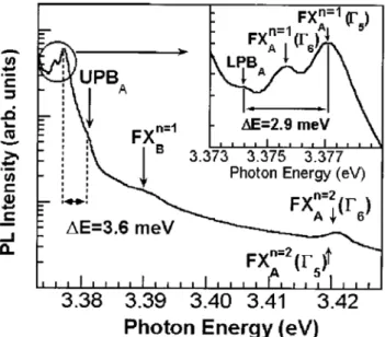
(44) Fig. 2-5 The electronic band structure of wurtzite ZnO. [unpublished]. Figure 2-6 displays the PL spectrum in the range of fundamental excitonic region measured at 10 K in the E⊥c polarization geometry for a high quality ZnO crystal. The A-free exciton and its first excited state emission are observed at FX An =1 = 3.3771 eV (3.3757 eV for Γ 6 ) and FX An = 2 = 3.4220 eV for Γ5 (3.4202 eV for Γ 6 ) band symmetry, respectively. Although, at k = 0, Γ 6 exciton is forbidden in the current measurement mode of polarization, it is still observable, due to the fact that the photon has finite momentum.. Geometrical effects such as not having the sample. orientation exactly perpendicular to the electric field may be also a reason for observing Γ 6 transition. Using the energy separation of ground state and excited state peak positions, the exciton binding energy and band gap energy can be predicted. The energy difference of about 45 meV gives an A-free exciton binding energy of 60 meV and a corresponding band gap energy of 3.4371 eV at 10 K.. Based on the. reported energy separation of the A- and B-free excitons (in the range of 9–15 meV), 28.
(45) we assigned the weak emission centered at 3.3898 eV, which is about 12.7 meV apart from the A exciton, to the B exciton transition.. Fig. 2-6 Free excitonic fine structure region of the 10 K PL spectrum for the ZnO single crystal. [14]. Additional fine structure of exciton lines was also observed in low temperature PL spectra. In strongly polar materials like ZnO transverse Γ 5 excitons couple with photons to form polaritons.. Therefore, as indicated in Fig. 2-6, the FX An =1 ( Γ 5 ). exciton line has two components.. The higher energy component at 3.3810 eV,. which is 3.6 meV apart from the A exciton, can be assigned to the so-called longitudinal exciton (upper polariton branch—UPBA).. The lower energy. component at 3.3742 eV, which is about 2.9 meV apart from the A exciton, corresponds to the recombination from the “bottleneck” region, in which the photon and free-exciton dispersion curves cross (lower polariton branch—LPBA). As a result, their dispersion curves are illustrated in Figure 2-7, and we will explain the energy diagram of a system consisting of a crystal and radiation below. Since Γ 6. 29.
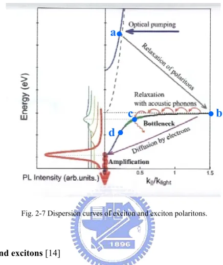
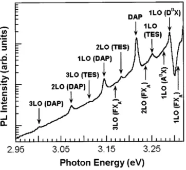
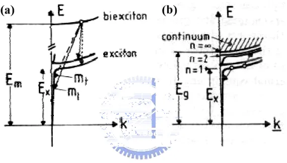
(46) excitons do not have transverse character, they do not interact with light to form polaritons, and thus have only normal free-exciton dispersion curves as seen in the PL spectra. The incident radiation in the exciton band region is converted to the exciton polariton inside the crystal and it has two modes, the upper and lower branches. The energy of the polariton is shown in Fig. 2-7 as a function of wave vector k. The broken line represents the relation between the energy and wave vector of the photon in vacuum.. The absorption of a photon creates an upper-branch polariton at a, which. is then scattered to state b of the lower-branch polariton. The polariton thus formed is thermalized from b to c through phonon and point-defect scattering.. The. thermalized polariton can be annihilated as a photon at d (direct radiative annihilation) or move in the crystal to be ionized or annihilated nonradiatively at imperfections, since the thermalized state has a longer lifetime. If the incident radiation energy is below the bottom of the upper-branch polariton, it generates the lower polariton directly. Here two assumptions are necessary. First, most inelastic scattering is caused by the LO phonon. Second, the probability for a thermalized exciton to be ionized or annihilated at imperfections is larger than that for it to be annihilated as a photon at d after being scattered from b to c. Under these assumptions if the energy difference between the upper polariton state a and the lower polariton state d is an integral multiple of the LO phonon energy, the cascade scattering of the polariton into state d occurs very efficiently and it is annihilated as a photon. If this energy difference is not an integral multiple of the phonon energy, the polariton is scattered and thermalized in the state near c in the lower-branch polariton and then it is ionized or trapped at imperfections before reaching state d. Thus the LO phonon structure is. 30.
數據
![Table 1-1 Properties of wurtzite ZnO. [1]](https://thumb-ap.123doks.com/thumbv2/9libinfo/8493603.184811/18.892.269.632.546.1053/table-properties-of-wurtzite-zno.webp)
![Fig. 2-5 The electronic band structure of wurtzite ZnO. [unpublished]](https://thumb-ap.123doks.com/thumbv2/9libinfo/8493603.184811/44.892.185.765.110.491/fig-electronic-band-structure-wurtzite-zno-unpublished.webp)
+7
![Fig. 2-8 Bound excitonic region of the 10 K PL spectrum for the ZnO single crystal. [14]](https://thumb-ap.123doks.com/thumbv2/9libinfo/8493603.184811/48.892.268.621.544.884/fig-bound-excitonic-region-spectrum-zno-single-crystal.webp)
![Fig. 2-9 10 K PL spectrum in the TES re on of the main bound exciton lines. [14]](https://thumb-ap.123doks.com/thumbv2/9libinfo/8493603.184811/50.892.269.622.358.686/fig-pl-spectrum-tes-main-bound-exciton-lines.webp)
相關文件
IQHE is an intriguing phenomenon due to the occurrence of bulk topological insulating phases with dissipationless conducting edge states in the Hall bars at low temperatures
The temperature angular power spectrum of the primary CMB from Planck, showing a precise measurement of seven acoustic peaks, that are well fit by a simple six-parameter
* All rights reserved, Tei-Wei Kuo, National Taiwan University, 2005..
The min-max and the max-min k-split problem are defined similarly except that the objectives are to minimize the maximum subgraph, and to maximize the minimum subgraph respectively..
Regardless of the assumed copula functions, we consistently find that the Chinese market experiences not only a higher degree of dependence but also a higher variation of
Moreover, due to the firm offers fixed years condition, we focus on this condition to introduce a two-stage game theoretical model which explicitly deals with
In this study, we report the preparation of metal Zinc (Zn) and Zinc oxide (ZnO) nanoparticles using an evaporation/condensation aerosol process via horizontal tube furnace
In the process control phase, by using Taguchi Method, the dynamic curve of production process and the characteristics of self-organizing map (SOM) to get the expected data
