國 立 交 通 大 學
電子工程學系電子研究所
碩 士 論 文
極紫外光輻射對於高介電常數介質之
影響研究
Effect of Extreme Ultra-Violet
Radiation on High Dielectric Constant
Dielectrics
研 究 生:李勃學
指導教授:崔 秉 鉞 教授
中華民國 九十九 年 七 月
極紫外光輻射對於高介電常數介質之影響研究
Effect of Extreme Ultra-Violet Radiation on
High Dielectric Constant Dielectrics
研究生:李勃學 Student: Po-Hsueh Li
指導教授:崔秉鉞 Advisor: Bing-Yue Tsui
國立交通大學
電子工程學系 電子研究所
碩士論文
A thesis
Submitted to Department of Electronics Engineering & Institute of Electronics College of Electrical and Computer Engineering
National Chiao Tung University in Partial Fulfillment of the Requirement
for the Degree of Master in
Electronic Engineering 2010
Hsinchu, Taiwan, Republic of China
極紫外光對於高介電常數薄膜之影響與其特性
之研究
研究生: 李勃學 指導教授: 崔秉鉞
國立交通大學電子工程學系 電子研究所碩士班
摘要
本論文探討極紫外光輻射對金屬閘極/高介電常數介電層的影響。選用氮化 鈦為金屬閘極材料,並選用五種介電層,分別為二氧化矽、金屬有機化學沉積之 氧化鋁、氧化鋁鉿、氧化矽鉿以及原子層沉積之氧化鋁,製作成金氧半(MOS)電 容器,另外也使用二氧化矽、氧化鋁兩種介電質製作了金氧半場效電晶體(MOSFET) 來驗證極紫外光對電晶體的影響。 以此五種介電質製作成的電容器經極紫外光照射後有明顯的電容-電壓特性 變化,包括平帶電壓飄移,電容-電壓曲線變形,也有遲滯現象的劣化。平帶電 壓飄移表示有淨正電荷產生,電容-電壓曲線變形表示介面能態增加,遲滯現象 劣化則表示邊界陷阱增加。綜合所有結果顯示二氧化矽抗極紫外光能力最佳。在 高介電常數介電質方面,氧化鋁呈現了最差之抗輻射能力。其中以金屬有機化學 沉積之氧化鋁有最大的平帶電壓飄移,原子層沉積之氧化鋁則顯現出較多的介面 能態以及遲滯現象增加。氧化矽鉿之能帶下半部經及紫外光照射後產生較多之介 面能態。氧化鋁鉿也對及紫外光有敏感的反應。以二氧化矽及氧化鋁作為介電質 的電晶體經極紫外光照射後,電晶體特性也和電容器一樣有臨界電壓漂移,此現 象可以呼應電容器電容-電壓曲線的漂移,顯示在介電層中一樣有電洞的捕捉。另外電晶體在關閉下的漏電流,經過元件的汲極、源極接面量測結果,我們可以 確定這是由源極以及汲極的 n+ -p 接面漏電所導致的結果。可能是因為場氧化層 (Field oxide)與矽基板介面經過極紫外光照射後,增加的介面能態導致激發電 流增加所致。 本論文也討論到經過極紫外光影響後的元件是否可以有自我修復的現象。元 件經由長時間儲存於一般室溫環境之下,電容器以及電晶體中因為極紫外光產生 的傷害會逐漸減少,並且有一定程度的改善,但是並無法回復到未照射前的性 能。因此極紫外光微影製程的設計必須與元件性能整體考慮,如何修復極紫外光 照射所產生的損傷也是企待進一步研究的課題。
Effect of Extreme Ultra-Violet Radiation on High
Dielectric Constant Dielectrics
Student: Po-Hsueh Li Advisor: Bing-Yue Tsui
Department of Electronics Engineering
Institute of Electronics
National Chiao Tung University
Abstract
In this thesis, EUV radiation damage on high dielectric constant (high-k) dielectric with metal gate is evaluated. TiN is selected as the metal gate electrode. Five kinds of high-k dielectric are evaluated. They are SiO2, , MOCVD Al2O3, HfAlO,
HfSiO and ALD Al2O3. Simple metal-oxide-Si (MOS) capacitor structure was
fabricated. We also use SiO2 and Al2O3 as gate dielectrics fabricate
Metal-Oxide-Silicon-Field-Effect-Transistor (MOSFET) in order to demonstrate EUV effect on MOSFET.
Before and after EUV irradiation, the C-V curves of these five dielectrics have significant change. There are flatband voltage shift, C-V curve distortion and hysteresis increases. Among these five kinds of dielectrics, SiO2 exhibits the best
EUV resistance. In high-k materials, Al2O3 suffered the worst radiation tolerance. The
MOCVD have the biggest flat band voltage shift and ALD Al2O3 exhibits more
more interface state in lower Si band gap. The HfAlO also has sensitive EUV irradiation response. The radiation hardness of all dielectrics may be related to hole traps in the dielectric and the EUV absorbing rate. Positive charges (hole traps) and border traps were also generated during EUV exposure.
The Id-Vg curve shows that there are Vth shift in both SiO2 and Al2O3 samples
which can respond to C-V curve shift with the positive charges be trapped in gate dielectric. We also observed when MOSFETs are in the off-state, the leakage current will raise after EUV irradiation. Measuring the n+-p junction I-V characteristic we find out the leakage current is also affected by EUV. We infer that the edge of S/D region under isolation generated leakage path after EUV irradiation which cause the leakage current when MOSFETs are in off-state.
In this thesis we also discuses that weather the device can have self-annealing behavior after EUV irradiation. After storage the samples at room temperature for a long time, the decreasing of radiation induced damages is observed. How to fixed the radiation damage is still under researched.
誌謝
碩士的生涯很快的已經進入了結束的階段,一路上隨著波折不斷的實驗,也 讓我從懵懂無知漸漸的蛻變並且茁壯堅強。在這短短的兩年之中我得到了許多人 的協助以及鼓勵。謹以此文來表達我無限的感謝。 首先我必須感謝我的指導老師 崔秉鉞老師。老師有著豐富的學識、一絲不 苟的處事態度、正直的品格、以及在教學上的熱誠。這些不凡的氣質,讓我對老 師有著由衷的欽佩。在老師的指導下,嚴謹的思考模式、扎實的訓練讓我的碩士 旅程得到比別人更多的收穫。在論文方面老師不厭其煩的一次一次、一字一字的 幫我修改眾多的錯誤,也讓我相當的慚愧。爾今以後我將會謹遵老師的諄諄教誨 前往未來的旅程。 再來實驗室的博班學長謝志民、盧季霈也時常的給我實驗的討論以及建議; 還有李振銘學長在機台訓練、實驗進行、結果討論都給予大力且無私的協助讓我 相當感動。李振欽學長、張孝瑜學姊也是提供了不少的實驗經驗。還有上一屆的 學長賴瑞堯、王俊凱、余昆武以及蔡依成也是在機台訓練上出了不少的力,並且 在平凡無奇的研究日子中帶來了很多的樂趣。實驗室的同學顏志展也和我一起做 著我們前無古人的研究,並且度過一次又一次漫長又難熬的實驗時程,同甘且共 苦。室友兼實驗室同學的羅子歆還有風趣幽默的周智超也在學業方面互相的砥礪 精進。鄭嶸健、王培宇、陳璽允、蘇婷婷、張克勤等學弟妹們也為我帶來了許多 的歡笑。另外國家同步輻射中心的許博淵博士、傅皇文先生還有彭均婷小姐也在 實驗儀器的架設提供了相當多的協助;奈米中心的技術員們也相當熱心的幫助我 完成我的實驗。 最後我必須感謝的是我最親愛的家人。父親 李其祐先生以及母親 石楣榕女 士提供了我一個安詳穩定的環境,讓我在這無後顧之憂這環境之中求學、成長。 感謝哥哥以及弟弟兄弟間的關照,更讓我覺得溫暖。 最後我將此文獻給一路上伴隨我、鼓勵我、協助我的大家。Contents
Abstract (Chinese)………I Abstract (English)………...………...III Acknowledge(Chinese)………V Contents………..VI Table Captions……….VIII Figure Captions……….IX Chapter1 Introduction1-1 The Evolution of Lithography………..1
1-2 Radiation Damage………... 3
1-2-1 Radiation Induce Charge Generation and Transport ………...3
1-2-2 Radiation Effects on MOS Devices and Circuits……… 4
1-3 Metal Gate and High-κ Dielectric………..5
1-3-1 From poly-Si Gate to Metal Gate……… 5
1-3-2 From SiO2 to High-κ material ……….7
1-4 Thesis Organization……… 9
Chapter2 Experimental Procedure 2-1 High-k Metal gate MIS Capacitor Fabrication ……….13
2-2 MOSFET Fabrication ………14
2-2-1In-situ Measurement Setup ……….15
2-3 EUV Source and End Station Setup ………..16
2-4 Dit and Oxide Trap Measurement ………..18
Chapter 3 Results and Discussion 3-1 Introduction………27
3-2 EUV Irradiation on MIS capacitors………..…….27
3-2-4 Recovery Property………. 34
3-2-5 In-situ Measurement versus Ex-situ Measurement ………37
3-3 EUV Radiation on MOSFETs ………...38
3-3-1 Basic Electrical Characteristics ……….38
3-3-2 Dose Effect……….39
3-3-4 Leakage Current Mechanism ……….39
3-3-5 Self-Annealing with time ………...40
Chapter 4 Summary and Future Works 4-1 Summary………... 68
4-2 Future Works ……….69
Table Captions
Chapter 3Table 3-1: Different MIS capacitors dielectrics fabricate condition and
properties ………... 42
Table 3-2: The different response of interface states, oxide traps and hysteresis in different material after EUV irradiation. ………..42
Figure Captions
Chapter1
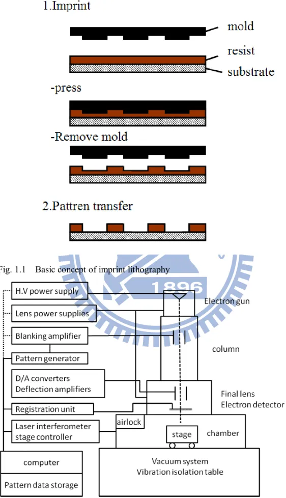
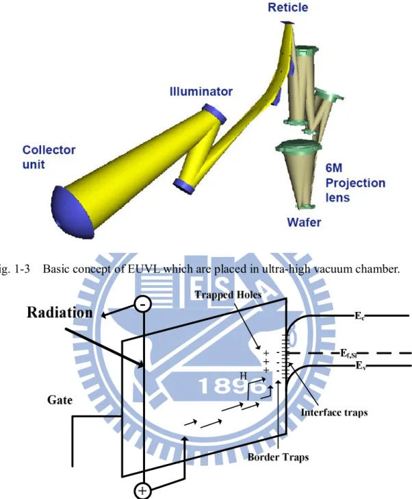
Fig. 1.1: Basic concept of imprint lithography………...………...…………...………10 Fig. 1.2: Outlook of maskless lithography system …………...………...…10 Fig. 1-3: Basic concept of EUVL which are placed in ultra-high vacuum
chamber .………...……..11 Fig. 1-4: Band diagram of gate oxide which is effected by radiation. Charge trapping
on the gate dielectrics and some defect traps are generation. ……...………11 Fig. 1-5: Band diagram of poly-si gate depletion. …...………..…..12 Fig.1-6: High-Performance Logic: The simulated gate leakage current versus limit gate leakage current for SiON (ITRS 2007 PROCESS INTEGRATION, DEVICES, AND STRUCTURES page.13) ………..………12
Chapter2
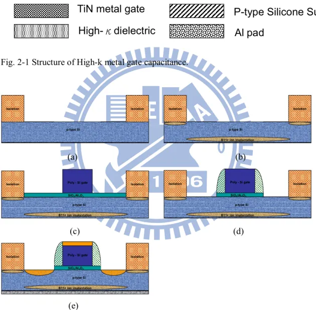
Fig. 2-1: Structure of High-k metal gate capacitance. ………...……...………...21 Fig. 2-2: Cross section view of the device after main process. (a) Isolation oxide formation (b) B11+ ion implantation (c) Poly-Si gate pattern (d) Spacer
forming (e) Source/Drain forming and Al deposition ………..21 Fig. 2-3: Process of in-situ measure sample. (a)Al2O3 (15nm) and TiN (40nm)
deposition (b) capacitance region etching (c) Bonding Al pad formation…...22
Fig. 2-4: Top view of in-situ measure sample………...……… 23 Fig. 2-5: The system module of the experiment chamber…………...……… 23
Fig. 2-6: (a) Photo of the experiment champer. (b) The output port position connect with measure system 4284b. ……… ………24
Fig. 2-7 : Smiling shape of bean line and the size is 0.016 cm2 ………..25 Fig. 2-8: Outlook of sample rod which is connect to the in-situ measure sample…...25 Fig.2.9: (a) Band diagram of flat band voltage (b) Band diagram of mid gate
voltage. ….………..26
Chapter3
Fig. 3-1: High-frequency C-V curve of MIS capacitor with TiN metal gate and SiO2
insulator at 100 kHz. ………...43 Fig. 3-2: High-frequency C-V curve of MIS capacitor with TiN metal gate and
MOCVD Al2O3 insulator at 100 kHz………....43
Fig. 3-3: High-frequency C-V curve of MIS capacitor with TiN metal gate and HfSiO insulator at 100 kHz. ………...44 Fig.3-4: High-frequency C-V curve of MIS capacitor with TiN metal gate and HfAlO
insulator at 100 kHz. ………...44 Fig. 3-5: High-frequency C-V curve of MIS capacitor with TiN metal gate and ALD
Al2O3 insulator at 100 kHz. ………...46
Fig. 3-6: Cross section of MOCVD Al2O3 with IL and rough surface between the
TiN...46 Fig. 3-7: Cross section of ALD Al2O3 without IL and smooth between the TiN...45
Fig. 3-8: Comparison of non-annealed and annealed High-frequency C-V curve of TiN + ALD Al2O3 capacitor after 300oC 30mins in high-vacuum furnace...47
Fig. 3-10: High-frequency C-V curve of TiN+SiO2 capacitor with EUV iradiation
dosage at 444mJ/cm2 and 1800mJ/cm2. ……… 48 Fig. 3-11: High-frequency C-V curve of TiN + HfAlO capacitor with EUV irradiation
dosage at 55.12 mJ/cm2 and 275mJ/cm2. ……….……... 48 Fig. 3-12: High-frequency C-V curve of TiN + MOCVD Al2O3 capacitor with EUV
irradiation dosage at 55.12 mJ/cm2 and 275mJ/cm2……….49 Fig. 3-13: High-frequency C-V curve of TiN + HfSiO capacitor with EUV irradiation
dosage at 55.12 mJ/cm2 and 275mJ/cm2. ……….…49 Fig. 3-14: High-frequency C-V curve of TiN + ALD Al2O3 capacitor with EUV
irradiation dosage at 55.12 mJ/cm2 and 275mJ/cm2. ………50 Fig.3-15: High-frequency C-V curve of in-situ TiN + ALD Al2O3 sample with EUV
irradiation dosage from 55.12 mJ/cm2 to 1102.4 mJ/cm2………50 Fig. 3-16 Comparison of interface trap density as a function of surface potential between Pre-irradiation and after 1800mJ/cm2 dosage for (a) SiO2 and
275mJ/cm2 dosage for (b) HfSiO, (c) HfAlO, (d) ALD Al2O3 and (e)
MOCVD Al2O3 sample………53
Fig. 3-17(a): Recovery behavior of ALD Al2O3 sample after 275mJ/cm2 EUV
irradiation for forward sweep high-frequency C-V curve……….54 Fig. 3-17(b): Recovery behavior of ALD Al2O3 sample after 275mJ/cm2 EUV
irradiation for reverse sweep high-frequency C-V curve………..54 Fig. 3-18: High-frequency C-V curve of SiO2 sample recovery behavior from 4.8x10³
s to 4.66x10⁶ s after 1800mJ/cm2 EUV irradiation………55 Fig. 3-19: High-frequency C-V curve of MOCVD Al2O3 sample recovery behavior
from 7.2x10² s to 4.92x10⁶ s after 275 mJ/cm2 EUV irradiation………...55 Fig. 3-20: High-frequency C-V curve of HfSiOsample recovery behavior from 3x10² s to 2.8x10⁴ s after 275 mJ/cm2 EUV irradiation………..….56
Fig. 3-21: High-frequency C-V curve of HfAlOsample recovery behavior from 3x10² s to 3.6x10³ s after 275 mJ/cm2 EUV irradiation………...56 Fig. 3-22(a): Hysteresis voltage, ΔVfb and ΔVmg as a function of time of SiO2
sample………...57 Fig. 3-22(b): The ΔNit values as a function of time of SiO2 sample………57
Fig. 3-23(a): Hysteresis voltage, ΔVfb and ΔVmg as a function of time of MOCVD
Al2O3 sample………..58
Fig. 3-23(b): The ΔNit values as a function of time of MOCVD Al2O3 sample…….. 58
Fig. 3-24 (a): Hysteresis voltage, ΔVfb and ΔVmg as a function of time of HfSiO
sample.……….. 59 Fig. 3-24(b): The ΔNit values as a function of time of HfSiO sample. ………...59
Fig. 3-25(a): Hysteresis voltage, ΔVfb and ΔVmg as a function of time of HfAlO
sample. ……….………60 Fig. 3-25(b): The ΔNit values as a function of time of HfALO sample. ……….60
Fig. 3-26(a): Hysteresis voltage, ΔVfb and ΔVmg as a function of time of ALD Al2O3
sample………...…61 Fig. 3-26(b): The ΔNit values as a function of time of ALD Al2O3 sample …………61
Fig. 3-27: Difference response of high-frequency C-V curve between in-situ and non ex-situ ALD Al2O3 samples under close EUV irradiation dosage………. 62
Fig. 3-28: Basic characteristic Id-Vg curve of SiO2 and Al2O3 MOSFET…………... 62
Fig. 3-29: Id-Vg curve of SiO2 MOSFETs with different EUV irradiation dosage from
195mJ/cm2 to 4680mJ/cm2 (Vd=0.1)……… 63
Fig. 3-30: (a) Swing and Vth of SiO2 MOSFETs as a function of EUV dosage. (b)
Fig. 3-32: Id-Vg curve and Is-Vg of SiO2 MOSFETs………... 64
Fig. 3-33: Junction current before and after 1170mJ/cm2 EUV irradiation. …………65 Fig. 3-34 The schematic cross-sectional structure of EUV irradiation damage between isolation oxide and depletion region where the interface states are as generation centers. ………..65 Fig. 3-35: Id-Vg curve of SiO2 MOSFETs with storage in room temperature from 21hr
to 208hr after 4680mJ/cm2 EUV irradiation………. 66 Fig. 3-36: Leakage current of SiO2 as a function of time after 4680mJ/cm2 EUV
irradiation……….66 Fig. 3-37: Swing of SiO2 MOSFET as a function of time after 4680mJ/cm2 EUV
irradiation………. 67 Fig. 3-38: The Vth of SiO2 MOSFET as a function of time after 4680mJ/cm2 EUV
Chapter1
Introduction
1-1 The Evolution of Lithography
VLSI technology has been developed since 1970s, the technology becomes more and more complex and hard to follow Moore’ law. There are many issues limiting VLSI technology such as gate oxide quality, source/drain resistance, short channel effect, and so on. But in the latest decade, lithography system has dominated the scaling down speed. If there had any chance to make more delicate pattern, VLSI technology could progress much easier. From the first contact Aligner machine to G-line stepper, I-line stepper, 248-nm stepper, and 193-nm stepper/scanner, every change of exposure wavelength pushed the CMOS technology. However the 157-nm wavelength machine is so expensive and does not improve too much in line width and pitch, every company and fundamental research has turn to build 193-nm immersion machine. According to the 2009 ITRS [1], the 193-nm immersion machine with water can fabricate 45 nm pitch, and many company has made it into commercial production. Furthermore, the 193-nm immersion machine with double or even multiple pattern technique may be the next generation technology in 22 nm technology node, however it has not been proven that the 193-nm optical solutions are available beyond the 22 nm node. There must be a new method, a powerful method to deal with future technology nodes.
technologies have huge difference comparing with the traditional lithography technology so they all have their own problems and advantages. Imprint Lithography is a technology makes template press on a thin film or on resist to make pattern, as shown in Fig. 1-1. In the previous work, imprint lithography can reach 14 nm pitch or even 5 nm linewidth [2]. However, how to make infrastructure for the 1X technology templates and a totally defect-free imprint templates are big problems. Maskless Lithography has been developed since 1980’s. It use electron or molecule beam to make resister been exposed, as shown in Fig. 1-2. Electron and molecule is not a light, as long as one can make the beam smaller, it could make smaller pitch and line width. But the major problem of the Maskless Lithography is the wafer throughput. The commercial wafer throughput should be 200-300 wafers/hr, but e-beam lithography is far away from this requirement. Maybe Multi-beam systems could solve this problem in the future.
Comparing EUVL with the above two method, EUVL is also a promising lithography system and have ability to be the next generation system. The Netherlands company ASML had presented the EUV alpha-demo machine and AMD, IBM, and Toshiba used this machine to fabric 22nm node device successfully [3]. EUVL use 13.5nm wavelength as the light source, the light even close to X-ray, it also been called soft X-ray. The wavelength in this section has very high absorption rate in most materials, so the system needs to be operated in high vacuum. All optical systems should use defect-free reflective lens which reflect light by means of interference, and using reflection mask, as shown in Fig. 1-3. Because the EUVL has many differences compared to the 193-nm immersion system, there are some problems waiting for solving such as source power>180W, zero printing defect mask blanks, and some resist issues. All of these problems have been researched for a lone time. It is believed that these problems will soon be solved and the EUVL would be ready to go.
Although it is expected that EUVL will be used in the next generation, the EUV damage on advanced devices is a potential concern. It should be notice that the energy of EUV is 91.85 eV, which is several times of the SiO2 band gap. The high energy
photons may induce electron-hole pairs in the gate dielectric, and results in threshold voltage shift and device variation as well as reliability issue. Radiation damage should be taken into serious consideration. All of these problems are not so obvious in previous technology nodes because the energy of the 193-nm wavelength is only 6.42eV. As we introduce EUVL into fabricate process, radiation damage should be considered caerfully.
1-2 Radiation Damage
The original motive of radiation damage can trace back to the malfunction of Telstar I communication satellite in 1962, however, radiation damage was fully studied science 1970’s. As the semiconductor devices were used from 1970’ in the field of outer space, airplane, national defense industry, nuclear weapon, and high energy physics, the reliability of semiconductor devices in such harsh environment was noticed and we should take it much more carefully. Today, in the semiconductor process, there are many radiation damage sources those we also should be care of.
1-2-1 Radiation Induce Charge Generation and Transport
Radiation damage is caused by high energy ions or high energy photons which will generate mobile electrons and holes in both the silicon substrate and the insulator in MOS devices and cause some kinds of damages in the devices. The most sensitive
generate electron-hole pairs (e-h pairs) in the oxide. Most of the e-h pairs will recombine in several picoseconds. The other fraction of electrons and holes will be swept by the electric field. The electrons generated by radiation are much more mobile than the holes, it will be transferred away from oxide. The holes also been transferred by electric field toward the dielectric/Si substrate interface. However, the immobile holes undergo a rather dispersive hopping through the oxide. Eventually, some of the holes will be captured by hole-traps, and results in negative threshold voltage shift which can persist from hours to years. Interface states can be generated by radiation. There are many models have been proposed to describe the action, the most widely used model are hydrogen model, injection model, and stress model [4-10], but none of them can describe all phenomena. In the previous stage of radiation damage studies, most of them focused on the damages in SiO2 which is the
gate dielectric of traditional MOSFETs. In recent years, high dielectric constant (high-k ) dielectric and metal gate have been employed since the 45 nm technology node and the radiation damage in high-k material should also be evaluated. High-k materials have been proved that they have much severe charge trapping problem then SiO2 due to the high density of intrinsic defects [11-14]. There is increasing interest of
radiation hardness of high-k materials as it replaces SiO2 as the gate dielectric.
1-2-2 Radiation Effects on MOS Devices and Circuits
After irradiation, most characteristics of MOSFETs will be changed. These degradations such as threshold voltage shift, leakage current increase, swing degradation, DIBL degradation, and GIDL increase [15] make designer hard to have characteristics in hand. Even worse, all of these characteristics will change with time. When designer design the circuits, they have to make some trade-off on performance and work margin to make sure circuits will not malfunction. Radiation effects on
MOSFETs not only relate to materials but also relate to the device geometry, substrate type, method of fabrication, and structure. Besides, LOCOS isolation, shallow trench isolation, P-N junction, parasitic BJT, or even parasitic MOSFET [16-18] which around MOS devices would also be affected by radiation and have side effects on integrated circuits.
1-3
Metal Gate and High-κ Dielectric
1-3-1 From poly-Si Gate to Metal Gate
Metal gate MOSFETs was used at the beginning of the semiconductor industry. In that stage the gate electrode of MOSFETs was mad of Al. However, Al metal gate has a major disadvantage: the low melting point (660℃). Due to the low melting point, Al could not sustain high temperature process such as activation annealing of source/drain (S/D) dopants. Therefore, S/D must be formed before gate patterning. To make sure there is sufficient overlap between gate and S/D, the design rule of gate to S/D overlap can not scale down which results in high gate to S/D overlap capacitance. Gradually, Al gate was replaced by poly-silicon gate. Poly-Si gate was chose because it could be used in self-aligned process. Moreover, high melting point, low thermal stress, and fewer interface state in oxide/silicon also make the process much easier to be implemented and controlled.
However poly-Si gate encounters some problems. In order to reduce RC delay, the sheet resistance of poly-Si gate must be reduced, but the solid-state solubility of dopant in silicon has its limitation that makes sheet resistance could not be reduce
other problem is that boron may penetrate to channel from p+ poly-Si gate. When the process temperature exceed 800℃ [19] , the dopants in the p+ poly-Si gate diffuse into the substrate and cause fixed charge in the gate oxide. Moreover, the penetrated boron will change the substrate concentration. All of these side effects make the threshold voltage shift and difficult to be controlled. Although this problem can be relaxed by using amorphous Si gate, SiGe gate, or incorporating nitrogen in gate oxide, they could not totally be solved.
The major problem which make poly-Si gate been ruled out is the depletion region in the poly-Si gate. This is also cause by the limitation of solid solubility in the Si [20]. In fact, the active dopant concentration must be higher than 1.87×1020 cm-3, at 25-nm gate length technology [21]. However, this presents great difficulty science the activated dopant concentration in poly-Si saturate at 6×1019 cm-3 and 1.0×1020 cm-3 for boron and phosphorus [22]. The depletion region in the gate electrode will degrade the channel potential, as illustrate in Fig. 1-5 [23]. This situation will make the equivalent gate oxide Thickness (EOT) could not continually scale down, even if there is already high quality thin gate oxide.
In order to make up for the shortcoming of poly-Si gate, metal gate seems to be a promising candidate for device under 45nm CMOS technology node. Metal gate provides low resistivity, high transconductance, improving mobility when high-k gate dielectric has been used [24, 25] to avoid boron penetration and gate depletion. Avoiding gate depletion could improve the gate controllability and reduce EOT. With all of these advantages, metal gate also have to deal with many old problems, high temperature in process, different gate work function on pMOS and nMOS, material stability, process compatibility, and reliability. By the time these problems have been solved and the poly-Si gate has been replaced.
1-3-2 From SiO
2to High-κ material
Gate controllability is a subject which we always want to improve. As the technology going forward, the industry demands higher performance device and higher device density, yet we could easily reach these goals by scaling down the thickness of gate dielectric. Increasing the gate capacitance Cox is the reason why we
want to scaling down the gate dielectric. From the simple model for MOSFET, the drive current could be written as
D D T G ox d )V 2 V -V -(V C L W I (1) , where W is the channel width, L is the channel length, μ is the channel carrier mobility, Cox is the capacitance density of gate underlying channel is in the inverted
state, VG is the gate bias, and VD is the drain bias. When the device is working in the
saturation region, VD= VG – VT and equation (1) could be written as
d,sat Cox(VG -VT)2 L W 2 1 I (2) Logic device’s performance depends on the Id,sat, and Cox could be promoted by
decreasing oxide thickness, for the reason ox 0 ox t k C (3) , where k is the dielectric constant, ε0 is permittivity of free space, and t is the ox
thickness of oxide. However t could not shrink forever. In the 2009 ITRS, it is ox pointed out that the EOT of the high-performance logic device should reached 1.1 nm in 25nm technology node [26][27]. The ultra thin oxynitride will not competent for the job as the gate dielectric [28]. We can see clearly in Fig. 1-6., the leakage current couldn’t be suppressed to desired level. The direct tunneling current will increase
In order to solve the above problems, there must be a material that has good gate controllability, low leakage current, and good reliability. Therefore, high-k material was introduced. We can understand the advantage of high-k material from equation (3). The high dielectric constant, which is higher than SiO2 (k=3.9), can reach the
same Cox level with thicker physical thickness. High-k material with thick physical
thickness can not only reduce direct leakage current but also have better reliability compared with ultrathin oxide. Many high-k materials have been proposed. Ta2O5
[30][31], SrTiO3[32][33][34], and Al2O3[35][36] were been nominate for its have
applied in the DRAM memory capacitor for many years and the high dielectric constant from 10-80. However, Ta2O5 and SrTiO3 materials are not
thermodynamically stable in direct contact to Si [16][37][38][39]. The dielectric constant of Al2O3 is not high enough which will make the EOT hard to scale down.
Comparing with Ta2O5, SrTiO3, and Al2O3, group IVB metal oxides show much
promise in all kinds of material. TiO2 [40][41], ZrO2[42][43] and HfO2[44][45] are
wildly study in this field because of their’s thermal stability, low interface state, suitable band offset and Gate compatibility [46]. Among these high-k materials, Hf-based dielectric has been used in the high performance logic device in Intel’s 45 nm technology [47][48].
As mentioned at the end of Section 1-2-1, the radiation damage on Al2O3 was
noticed science 1990’s [49] [50]. Using high energy X-ray, these researches are focus on the electrical degradation instead of using Al2O3 to replace SiO2 on VLSI
technology. Until 2000’s, the Hf-based dielectrics were mentioned and wildly researched for it’s potential to replace SiO2. J. A. Felix and D. M. Fleetwood et al.
study many radiation reactions on the Hf-based dielectrics, and Al2O3. The basic
experiments of these studies followed the radiation damage on SiO2 researches and
SiO2. Because EUV is a high energy source, when EUVL is introduced into mass
production, the radiation hardness of these high-k materials should be reconsidered again.
1-4 Thesis Organization
In the first chapter of this thesis, we have briefly described the evolution of lithography system and also understand the EUV would be one of the most promising light source beyond 22 nm technology node. Since high-k and metal gate structure has been used in CMOS technology, EUV irradiation damage on high-k material should be concerned. Literatures regarding to ionized radiation damages on high-k material are also reviewed in this chapter.
In chapter 2, the fabrication process of MOS capacitor with various high-k dielectrics using TiN as gate electrode and traditional MOSFET will be described in detail. We also describe how to build up the experimental chamber and environment which we used in the National Synchrotron Radiation Research Center (NSRC). At the end of chapter 2, the method which is used to analyze the interface density is explained.
In chapter 3, the basic character of MOS capacitance will be shown. It is demonstrated that after EUV illumination the device suffers from some damages and degradations. Traditional MOSFET and MOSFET with high-k/metal gate are compared. It is also observed that EUV also damages the isolation region and cause higher S/D junction leakage current. .
At the end of this thesis, conclusions, future works, and some advices will be addressed.
Fig. 1.1 Basic concept of imprint lithography
Fig. 1-3 Basic concept of EUVL which are placed in ultra-high vacuum chamber.
Fig. 1-4 Band diagram of gate oxide which is effected by radiation. Charge trapping on the gate dielectrics and some defect traps are generation.
Fig 1-5 Band diagram of poly-si gate depletion.
Fig.1-6 High-Performance Logic: The simulated gate leakage current versus limit gate leakage current for SiON (ITRS 2007 PROCESS INTEGRATION, DEVICES, AND STRUCTURES page.13)
Chapter2
Experimental Procedure
In this thesis we have prepared two kinds of samples for our experiment: high-k/metal gate MIS capacitors and high-k/poly-Si gate MOSFETs. The ideal work function of MOSFETs should be near the Si conduction band for NMOS and valence band for PMOS. For high-k/metal gate MIS capacitors, we choose TiN as the gate electrode because it is a midgap metal and is suit for adjusting PMOS and NMOS threshold voltage. TiN also have the good ability to screen low-energy surface optical phonon which was reported for mobility degradation under channel inversion condition [24][25]. HfSiO, HfAlO and Al2O3 are used as the gate dielectric and SiO2
is used as reference. A 40-nm-thick TiN is designed for EUV to penetrate into gate dielectric. In order to have appropriate radiation damage that can be detected easily, the thickness of gate dielectric is chosen as 15 nm. The MOSFETs use poly-Si/SiO2
and poly-Si/Al2O3 as gate stacks. We also prepared TiN/Al2O3 capacitor as the in-situ
measurement sample which could measure directly during EUV illumination.
2-1 High-k Metal gate MIS Capacitor Fabrication
Fig. 2.1 shows the structure of the high-k/metal gate MIS capacitor. The devices were fabricated on 6-inch p-type Si wafer with resistivity of 1~10 Ω-cm. The wafers were first marked by a laser-marker system and then were cleaned in SC1 for 10 min to remove particles. Then the wafers were cleaned using the stander RCA cleaning
Si(Otbu)2(mmp)2, and Al(isopropoxide)3as precursors and Ar as carrier gas in O2 gas
surround, the high-k dielectric were deposited at 500C. The pressure during deposition was 5 mbar and the thicknesses were about 15 nm. There was also a 15-nm-thick SiO2 growing thermally by a furnace system at 900C as the control
sample. The 40nm TiN metal gate was deposited by a sputtering system and was patterned by RIE etching. The samples were then sputtered Al on back side by an e-gun system as the backside contact. After a 300C /30min annealing process, the capacitor samples were finished.
2-2 MOSFET Fabrication
Fig. 2.2 shows the main process flow of the n-channel MOSFET. The devices were fabricated on 4-inch p-type Si wafers with resistivity of 1~10 Ω-cm. Wafers were cleaned by standard RCA cleaning process first and then a 500-nm-thick SiO2
was thermally grown at 1000C by a furnace system. We used I-line stepper to define the active region and used buffered oxide etchant (BOE) to open the active region as shown in Fig. 2.2(a). After removing the photo-resist by SPM (H2SO4 : H2O2 = 3 : 1),
a SiO2 film was thermally grown at 900C by dry oxide to 15-nm-thick as a sacrificial
layer. B11+ ion implantation at 145 keV to a dose of 1x1013 cm-2 was performed to
enhance the field SiO2 isolation as shown in Fig 2.2(b). Then, the sacrificial layer was
remove by DHF (HF:H2O=1:100). There are two kinds of gate dielectrics : SiO2 and
Al2O3. The SiO2 was thermally grown at 900C by dry oxidation to 15 nm and the
Al2O3 was deposit by an atomic layer deposition (ALD) system using Al(CH3)3 (TMA)
and H2O as precursors. The Al2O3 was deposited at 300C and the thickness is also 15
nm. The following step was deposition of 150-nm-thick undoped poly-Si film by a low pressure chemical vapor deposition (LPCVD) system. The temperature of
LPCVD was 620C and the pressure was 100mtorr. And then the poly-Si gate electrode was patterned by I-line stepper. The gate etching used a high density plasma reactive ion etching (HDP RIE) system and the etching stopped at the dielectric film as shown in Fig 2.2 (c). After forming the SiO2 spacer as shown in Fig 2.2(d), P31+
was implanted at 35 keV to a dose of 5x1015 cm-2. Gate and source/drain dopant activation was performed by rapid thermal annealing (RTA) at 900C for 20 seconds in nitrogen gas ambient. After Al deposition by E-gun on the wafer back side, the device fabrication was finished as shown in Fig 2.2(e).
2-2-1In-situ Measurement Setup
In order to set up the in-situ measured system the sample should connect with outer PVC circuit board by Au wire. The Au wire bonding point cannot bond directly on the gate because the gate oxide would be damage by the bond machine. The bonding position should be on the field oxide region.
The main process of the in-situ measurement sample is shown in Fig. 2-3. In-situ measurement samples were fabricated on 4-inch p-type Si wafers with resistivity of 1~10 Ω-cm. A 500-nm-thick SiO2 was thermally grown at 1000℃ by furnace to be
field oxide. After patterning the active region, Al2O3 were deposited on the wafers by
an ALD system with the precursor Al(CH3)3 (TMA) and H2O at 250℃. Then, TiN
was deposited for 400Å thickness by sputter (Fig. 2-3(a)). The gate was patterned by I-line stepper and etched by HDP-RIE (Fig. 2-3(b)). Al pad was formed by lifted-off method as shown in Fig. 2-3(c). Finally the sample was deposited with Al on the back side and annealed at 300℃ for 30min.
sample and circuit board are bonded together by Au wire. The circuit board will contact to the pin as the top electrode.
2-3 EUV Source and End Station Setup
There are many ways to produce EUV such as discharge produced plasma (DPP), laser produced plasma (LPP) and synchrotron radiation [52]. Compared to DPP and LPP, synchrotron light source have some benefits for our study. The synchrotron light is a pure light which means that it has no contamination issue and the light also has extreme narrow band width of about 0.01 % which suits ultra thin film measurement and EUV multilayer optical component test. However synchrotron light is not fit mass production for its power is only 0.5 W which is far away from mass production power of 180W. The main reason for commercial machine needs 180W source power is that many optical components decay the source power inside the system. As EUV reach wafer surface, the power of EUV would be less than 1 % of the source power. There is no so much decay in the synchrotron system so that the synchrotron system can have lower power. In this thesis, we use synchrotron radiation generated EUV source provided by the National Synchrotron Radiation Research Center, Taiwan (NSRRC) and the beam line numbers are BL08A and BL21B.
The end station we used in this experiment consists of two parts: main chamber and differential chamber. These two chambers are separated by a valve. Both chambers should be pumped down to a pressure about 10-8~10-7 torr during the experiment. The main chamber is the place where we put the sample in and the differential chamber allows that the pressure of main chamber doesn’t keep at such a high vacuum. The EUV light is generated by synchrotron radiation and be focused by the beam line. Then the light passes through the differential chamber and finally
reaches the main chamber and irradiates on the sample. The outlook of the whole system is shown in Fig.2-5 and Fig 2-6. Fig. 2-5 shows the module of the whole experiment system. Turbo pump 1 and turbo pump 2 provide the high vacuum environment at main chamber and differential chamber, respectively. Rough pumping is done by scroll pump .Fig. 2-5(a) is the photo of our system and Fig2-5 (b) shows the output port position, through which the in-situ measurement sample can be connected to the measure instruments.
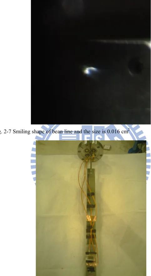
The shape of the beam is a smiling shape (Fig 2-7) and the size is 0.016 cm2. Using photo diode we can transfer the photocurrent into EUV flux. The structure of sample rod is shown in Fig. 2-8. Sample can be directly stuck on the rod by copper foil or carbon foil. In this thesis, it is found that there still have some damages on the devices even if the devices are not directly irradiated by EUV. To avoid this issue, sample can be stuck behind a steal plat with a small window. Through the window, only the devices to be tested would be irradiated. The following is the stander steps of changing samples :
1. Check all the valve (V1 ,V2 and V3) and turbo pump 1 and 2 are close (The user should wait for 20-30 min after turn off the turbo pump to let the turbo pump slow down).
2. Vent the main chamber from the back turbo pump 1 with N2 gas purge.
3. Open the sample rod and take it out. 4. Stick the sample on the sample rod.
5. Load the sample rod into the main chamber and lock it off.
6. Open V2, the scroll will pump down the pressure of main chamber to 5x10⁻²
As the pressure of the main chamber is pumped down to 1x10⁻⁷ ~ 5x10⁻⁸ torr, sample is ready to expose to EUV. The EUV is invisible, so we use white light to help us to find the light position. The main irradiation processes are as follows :
1. Set the synchrotron light to white light.
2. Open beam line valve and make the white light to pass through differential chamber and incident in the main chamber
3. Using telescope to observe white light spot and set the telescope cross line on the light spot site.
4. Open beam line valve to block the white light and set light into EUV.
5. Move the sample to the telescope cross line (If one wants to observe the EUV directly, he can make the EUV spot on the fluorescent plate which is on the top of sample rod.)
6. Open beam line valve then EUV incidents on the sample and count down the expose time.
7. Turn off beam line valve to block EUV.
8. Go to Step 5 if there are other samples on the sample rod.
After the irradiation process is over, user can follow the changing sample steps to change the sample or finish the experiment.
2-4 D
itand Oxide Trap Measurement
High energy radiation will generate oxide charges and interface states. These damages may cause C-V curve shift and distortion. In this thesis we estimate these
interface density and oxide charge density by two methods: high-frequency C-V method (Terman method) [53] and Vfb and Vmid method. The theoretical C-V curve is generated
charges [54]: d ox C C C 1 1 1 ………...Eq.2.1 where ) / , ( ] 1 ) )[exp( / ( ) exp( 1 2 0 0 0 0 p p s s p p s D s s s d p n F p n L d dQ C ) / , ( s np0 pp0 F = [exp( ) 1] [exp( ) 1] 0 0 0 p p p p p p p n KT q p0 s 2 p0 s D qp q p kT L
The Cox can obtain from the C-V curve measurement in accumulation mode. The
substrate concentration also can get from the following equation:
N = −2 q ………Eq. 2.2 After shift the ideal C-V curve by Vfb which is extracted from the measured C-V curve,
the Dit can be calculated by comparing the measure C-V curve with the theoretical
C-V curve.
D = ( ) .…..……….. Eq. 2.3 , where ΔVG is the VG different between ideal C-V curve and measured C-V curve
under same capacitance and φs is the surface potential.
When the device is damage by radiation, we care about the change of oxide trap density (ΔNot) and interface state density (ΔNit) which are related to the charges and
and after irradiation). The extraction of ΔNot and ΔNit is much easier. The basic
assumption is that interface states in the upper half of the Si bandgap are predominantly acceptor-like, while those in the lower half of the bandgap are predominately donor-like [48]. 2 mg 1 mg mg V -V V ……….. Eq. 2.4 2 fb 1 fb fb V -V V ……….. Eq. 2.5 , where Vmg1 and Vmg2 stand for the mid gate voltage before and after radiation
damage, respectively, Vfb1 and Vfb2 are the mid gate voltage and flat band voltage
before and after radiation damage, respectively. Then the ΔNot and ΔNit can be easily
extracted by the following equations.
qA V C -Not ox mg ……….. Eq. 2.6 qA ) V -V ( C -Nit ox fb mg ……….. Eq. 2.7 The reason could be easily explained by Fig.2.9 (a) and Fig2.9 (b). As the gate voltage is at Vmg,only the ΔNot affects Vmg because the interface states are charge neutrality
by donor-like interface states and acceptor-like interface states. The ΔVfb is affect by
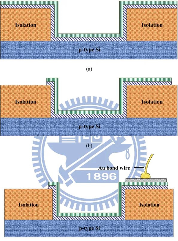
Fig. 2-1 Structure of High-k metal gate capacitance. p-type Si Isolation Isolation p-type Si Isolation Isolation B11+ ion implantation (a) (b) p-type Si Poly - Si gate SiO2/Al2O3 Isolation Isolation B11+ ion implantation p-type Si Poly - Si gate SiO2/Al2O3 Isolation Isolation B11+ ion implantation (c) (d) p-type Si Poly - Si gate SiO2/Al2O3 Isolation Isolation B11+ ion implantation (e)
Fig. 2-2 Cross section view of the device after main process. (a) Isolation oxide formation (b) B11+ ion implantation (c) Poly-Si gate pattern (d) Spacer
TiN metal gate
High-κdielectric
P-type Silicone Sub
Al pad
p-type Si Isolation Isolation (a) p-type Si Isolation Isolation (b) p-type Si Isolation Isolation Au bond wire (c) TiN Al2O3 Al
Fig. 2-3 Process of in-situ measure sample. (a)Al2O3 (15nm) and TiN (40nm)
Fig. 2-4 Top view of in-situ measure sample.
Fig. 2-5 The system module of the experiment chamber
Sample
Pin
Circuit board
Conductive copper foil
Glass
Thick wire
(a)
(b)
Fig. 2-6 (a) Photo of the experiment champer. (b) The output port position connect with measure system 4284b.
Fig. 2-7 Smiling shape of bean line and the size is 0.016 cm2
EC
Ei
EF
EV
Metal Oxide P-substrate
(a)
(b)
Chapter 3
Results and Discussion
3-1 Introduction
In this chapter, the characteristics of the MIS capacitors and MOSFETs with various gate dielectrics before and after EUV irradiation are investigated. From the C-V characteristics, the MIS capacitors with five kinds of dielectric are analyzed and discussed. The main process of these capacitors has been mentioned in the previous chapter. Table 3-1 lists the dielectrics used in this thesis and the processess how they were deposited. The radiation hardness on each dielectric by various doses, the magnitude of flatband voltage shift (ΔVfb) and mid-gap voltage shift (ΔVmg),
recovering with time, and leakage current are evaluated.
MOSFETs with two difference gate dielectrics are also examined in this chapter. As we know, the performance of MOSFETs mostly depends on the gate dielectric quality. Nevertheless, while irradiating by EUV, gate dielectric is the easiest part to be damaged. The every degradations of capacitor causing by EUV irradiation are also observed on MOSFETs. It is observed that the Vth shift and subthreshold swing
degradation are all correlated to the damages in gate dielectric. The difference of gate leakage current and off-state current between pre-EUV irradiation and post-EUV irradiation is observed.
capacitor area is 5.93x10⁻⁴ cm2. For the ALD Al2O3 sample, the capacitor area is
4x10⁻⁴ cm2. All of the C-V curves are measured by a precision LCR meter of model Agilent 4284B, the frequency of the small signal is set at 100 kHz and the magnitude is 25 mV.
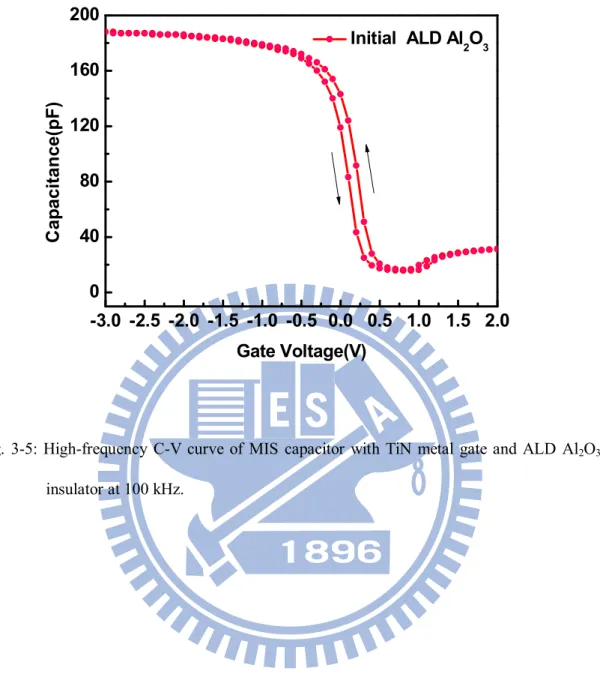
The initial C-V characteristics of the MIS capacitors with five different gate dielectrics are shown in Fig. 3-1 to Fig. 3-5. The flat band voltages of the SiO2,
MOCVD Al2O3, HfSiO, HfAlO and ALD Al2O3 samples are -0.26 V, +1.17 V, -0.09 V,
+0.66 V and +0.18V in sequence.
Hysteresis of C–V curve is commonly observed on high-k materials and it is also an important parameter to determine whether the high-k material can be used in MOSFET or not, so hysteresis needs to be minimized. Our SiO2 and MOCVD Al2O3
samples exhibit almost negligible hysteresis. However, on the HfSiO, HfAlO and ALD Al2O3 samples, significant hysteresis are observed. The magnitudes of hysteresis
are 0.09 V, 0.06 V and 0.124 V, respectively. Fig. 3-6 and Fig. 3-7 shows the TEM micrographs of the MOCVD Al2O3 and the ALD Al2O3, respectively. A 5-nm-thick
interfacial layer (IL) is observed on the MOCVD sample. This is because the deposition temperature of MOCVD is 500 oC. At this temperature, the high-k material can interact with the Si substrate. The composition of the IL is SiOx. Although the IL
quality is not good, it provides a better interface between high-k dielectric and Si substrate. The ALD Al2O3 sample suffers from the worst hysteresis, because there is
no IL at the interface. In fact, the hysteresis phenomenon could be reduced by RTA or another thermal process. Fig. 3-8 compares the C-V curves of the ALD Al2O3 sample
before and after annealing in high vacuum at 300 oC for 30 min. The hysteresis is reduced obviously after annealing. Therefore, all high-k samples discussed in the following are annealed at 300 oC for 30 min in high vacuum.
constant of 13.04, and follows by HfSiO, ALD Al2O3, MOCVD Al2O3 and SiO2. The
samples deposited by MOCVD have smaller dielectric constant then the theoretic value.
In Fig 3-6, it is obvious that the MOCVD Al2O3 sample have a rougher
TiN/Al2O3 interface then the ALD Al2O3 sample. The MOCVD Al2O3 sample also has
a thick IL at the Al2O3/Si interface which makes the MOCVD Al2O3 sample has a
large effective oxide thickness (EOT) and a lower dielectric constant.
3-2-2 Dose Effect
The exposure energy of EUV photo resist is suggested to be 10~20 mJ/cm2. The flux of the beam line 08A1 at NSRRC is about 1x10¹² photons/sec and the EUV energy is 91.85eV. Thus, the energy flux is 1x1012 x 91.85 x 1.6x10-19=0.0147 mJ/sec. The area of the EUV spot is about 0.016 cm2, so the irradiation dose rate is 0.918 mJ/cm2/sec1. In order to easily observe the irradiation damage, the EUV irradiation time is set to 60s and 300s which equals to 55.12 mJ/cm2 and 275 mJ/cm2, respectively. The SiO2 sample used beam line 21B2 and the flux of 21B2 is 1
mJ/cm2/sec.
The EUV beam spot are not so uniform. Fig. 3-9 (a) shows the 3 devices (on the same wafer) received EUV irradiation to a dose of 55.12 mJ/cm2 and the 4 devices (on the other sample) received EUV irradiation to a dose of 275 mJ/cm2. The C-V curves after EUV irradiation may distribute in a wide range due to the smiling shape EUV light spot shown in Fig. 3-9 (b). Therefore, the device with the most serious damage is selected to perform further analysis. In order to relax this problem for the
As has been mentioned in chapter 1, EUV is a high energy light source. The e-h pairs would be generated when the EUV incidents dielectric and the C-V curve will shift due to the trapped charges and distort due to the increase of interface states. Fig. 3-10 to Fig. 3-14 show the effect of EUV irradiation on various dielectrics. When the samples are irradiated by EUV, the C-V curves of all samples shift toward negative voltage direction, this means net positive charges are produced in the dielectrics. When the irradiation time is longer, the C-V curves shift more negatively. C-V curve distortion is also observed when the samples receive high dose irradiation.
As the dose increases, we can find an interesting phenomenon: hysteresis gets worse. Not only the high-k samples but also the SiO2 sample has this hysteresis
phenomenon. This phenomenon suggests that EUV irradiation may generate some slow traps and border traps. However it is believed that the increasing of border traps is the main reason for our samples [49]. Border traps are easily generated by radiation damage. These traps may charge and discharge when the gate bias changes. Eventually they cause the hysteresis of the C-V curve. In our experiments, it is found that high-k material is much easier affected by the EUV irradiation. It is also observed that more border traps are generated in high-k materials in comparison with in SiO2
dielectric. We could not make sure what kind of border traps are generated now (positive trap or negative trap). In the latter part of this chapter, we will discuss the self-annealing effect of the damages in dielectrics, some information will help us to distinguish what kinds of border traps are generated during EUV irradiation.
We use in-situ measurement to study the correlation between charge trapping and interface generation as the irradiation dose increases. Fig. 3-15 shows the in-situ measured C-V curve of the ALD Al2O3 sample. In the beginning of irradiation, the
ALD Al2O3 sample quickly traps positive charges and the C-V curve shifts toward
Al2O3 seems to slow down. At the same time, the interface state density still increases
quickly when dosage increases. The distortion of C-V curves in Fig. 3-14 is the evidence.
3-2-3 ΔV
fband ΔV
mgDifferent dielectrics have quit different responses to the EUV irradiation. It has been shown in Fig. 3-10~ Fig. 3-14 that different Vfb shifts are produced when the
dielectrics are irradiated by EUV to the same dosage at the beam line 08A1. After EUV irradiation, the ΔVfb of the SiO2 sample shows the lowest magnitude of only
-0.30V. The ΔVfb of the HfAlO, HfSiO, and ALD Al2O3 samples are -0.99 V, -0.9 V,
and -1.92 V, respectively. The MOCVD Al2O3 sample shows the worst ΔVfb of -2.39 V.
The ΔVmg values are also extracted. They are -0.23 V for SiO2 sample, -0.768 V for
HfAlO sample, -0.77 V for HfSiO sample, -2.24 V for MOCVD Al2O3 sample, and
-1.51V for ALD Al2O3 sample. From the Eq.2.4 and Eq.2.5, the ΔNot and ΔNit on etch
dielectrics can be calculated. These values are listed in Table 3-2. High-frequency method (Terman method) is also used to extract the energy distribution of the interface states before and after EUV irradiation. Fig. 3-16 shows the difference in the energy distribution of the interface states before and after EUV irradiation of all samples. It is obvious that after the EUV irradiation the interface state densities of all samples increase about one order of magnitude. And, the EUV generated interface states are donor-like and locate at the lower half of the energy gap of Si. . In Table 3-2, it is found that even if the MOCVD Al2O3 sample have the largest Vfb and Vmg shifts,
accumulation capacitances. From device point of view, MOCVD Al2O3 may suffer
from the worst device application, but from the material aspect, MOCVD Al2O3 is not
the worst dielectric on radiation hardness.
In Table 3-2, it is observed that after EUV irradiation the ALD Al2O3 sample
suffers from the worst hysteresis and ΔNit. However the MOCVD Al2O3 sample
suffers from the worst ΔVfb and ΔNot. From the TEM micrograph, it is known that
there is no SiO2-like IL on the ALD Al2O3 sample. Since the SiO2 sample exhibits the
best radiation hardness, the SiO2-like IL results in better radiation hardness so the ΔNit
of MOCVD Al2O3 sample is lower then that of the ALD Al2O3 sample. The ALD and
MOCVD Al2O3 samples both suffer from large ΔVfb than the other samples after EUV
irradiation. However, the MOCVD Al2O3 sample behaves worse than the ALD Al2O3
sample because the quality of ALD Al2O3 is better than the MOCVD Al2O3.
From the basic C-V curve measurements, it is observed that the SiO2 sample has
the best EUV hardness and the MOCVD Al2O3 sample is in the worst case. It is
known that the radiationhardness is related to many factors like e-h pairs generation rate, bonding energy, and original trap density, etc. In this thesis, we use the same irradiation dosage for each high-k dielectric and higher irradiation dosage for the SiO2, but SiO2 shows the best immunity to EUV irradiation. This result can be
explained by several reasons. First, SiO2 has the longest attenuation length (0.1 m)
in EUV range among these dielectrics. The attenuation length in SiO2 is about 5 times
longer than that in the other dielectrics. Owing to the longest attenuation length, SiO2
absorbs less energy from EUV and then less e-h pairs are generated in SiO2. Second,
the growth temperature of SiO2 is 900 oC, which is much higher than the deposition
temperatures of the other dielectrics. The higher deposition temperature results in less original trap density in the dielectric and then less EUV generated e-h pairs would be trapped. Third, the band gap of SiO2 is the largest. This property also makes e-h pairs
not generated so much.
For the high-k dielectrics, it is hard to predict their radiation hardness from a single factor. However, we can discuss the observed phenomena from two directions: charge generation and charge trapping. The amount of e-h pairs generated by EUV irradiation is the first essential factor. Total energy absorbed by dielectric, band gap, binding energy, and bond energy, ect., all of these factors determine the number of e-h pairs and eventually the number of charges may be captured in the dielectric. As we know, The band gap of Al2O3 is 8.8 eV and the band gap of HfO2 is 6 eV. The band
gap of HfAlO is between that of HfO2 and Al2O3 and the band gap of HfSiO is
between that of HfO2 and SiO2.When the same dose EUV irradiates on high-k
samples, the attenuation length affects e-h pair generation less than the band gap because the high-k materials have similar attenuation length from 0.02μm to 0.029μm. Finally, more e-h pairs can be generated in HfAlO than the others because HfAlO has the narrowest band gap. Even if sufficient e-h pairs are generated, charges must be trapped in the dielectric so that they can affect the C-V curve and can be detected. Intrinsic traps or radiation induce traps might be important factors in charge capturing. Combining all of these factors we observe the experimental result of flat-band shift is MOCVD Al2O3(-2.39V) >ALD Al2O3(-1.92V) > HfAlO(-0.99V) > HfSiO(-0.9V).
The ALD Al2O3 and MOCVD Al2O3 samples have the largest flat-band voltage shift
of -2.39V and -1.92V. This suggests that even if Al2O3 have less e-h pairs due to its
large band gap but it traps more charges. The trap density in the Al2O3 may be much
higher than the other high-k dielectrics. The overall radiation hardness depends on several factors. When we need to predict radiation hardness of a material, all factors must be taken into consideration.
3-2-4 Recovery Property
After EUV irradiation, the MIS capacitors are damaged to different levels, we are curious about if these damages are permanent or not? Can they be fixed by time or another ways? The recovery properties of the MIS capacitors are shown in Vfb, Vmg ,
and hysteresis, and are discussed as follows.
In the previous sections, it has been shown that after EUV irradiation, the hysteresis is getting worse, and it is known that the hysteresis is caused by border traps generated by EUV. Interface traps also increase as the irradiation dosage increases, and the interface states cause C-V curve distortion. It is curious that is there any way to know what kinds of traps are generated by EUV in each dielectric? Would it be the same for every dielectric? Fig. 3-17(a) and Fig. 3-17(b) shows the C-V curves of the ALD Al2O3 sample at various times after EUV irradiation. Fig. 3-17(a)
shows the C-V curves swept from negative voltage to positive voltage (forward sweep) and Fig. 3-17(b) shows the C-V curves swept from positive voltage to negative voltage (reverse sweep). We can combine these two figures into a full hysteresis loop. After EUV irradiation, the C-V curve distorts apparently and the hysteresis is getting worse. In Fig. 3-17(a) the distortion of the forward swept C-V curve quickly recovers in 2 hrs and the Vfb recovers to some extent. In this period, the reverse swept C-V,
shown in Fig. 3-17(b), almost does not change. These phenomena implies that donor-type interface states and border hole-traps are generated by EUV irradiation and these defects can be annealed gradually. The decrease of interface states density reduces the C-V distortion and the decreasing of border traps reduce the hysteresis. After 2 hrs, the C-V curve in forward sweep and reverse sweep shift in parallel. This means the decreasing of border traps and interface traps slow down, and the detrapping of the positive charges trapped in the dielectric dominates the C-V curve
shift.
Fig. 3-18 shows that the distortion and hysteresis of the C-V curve do not change with time and only C-V shift occurs on the SiO2 sample. These phenomena imply that
very few border traps are generated and the EUV generated interface states cannot recover at room temperature. In Fig. 3-19, the hysteresis of the MOCVD Al2O3
sample does not recover too much with time. But the distortion and shift of C-V curve reduces with time. These phenomena imply that the EUV irradiation generates both border traps and interface states in MOCVD Al2O3. The border traps do not recover
with time while the interface states and the trapped holes recover gradually at room temperature.
The recovery of C-V curve of the HfSiO sample is shown in Fig. 3-20. Sever distortion of the C-V curve after EUV irradiation is observed. The distortion at the upper half of the C-V curve indicates lots of donor-like interface states distributed at the lower half of the Si band gap. These interface states cannot recover at room temperature. EUV irradiation also generates border traps so that the hysteresis increases after EUV irradiation. Some border traps disappear in a few minutes but the remaining border traps do not decrease after 660 sec. Fig. 3-21 shows the C-V curves of the HfAlO sample with time. It is interesting that after EUV irradiation, negative border traps are generated. This is quite different from the other sample on which positive border traps are generated. Part of the border traps disappears in 600 sec. However, the remaining border traps, interface states, and trapped positive charges do not change up to 3600 sec.
Figure 3-22(a) ~ Fig. 3-26(a) show the flat band voltage and mid-gap voltage as a function of storage time at room temperature. It is clear that the shifts of flat band
mainly due to hole trapping. The trapped holes in dielectrics are not stable, they will detrap to substrate and/or gate or neutralized by electrons from substrate and/or gate. Therefore, the main reason of Vfb and Vmg recovery is the vanish of the trapped holes,
we find all C-V curves will come closer and closer to the original curve with time. Immediately after EUV irradiation, the whole dielectric is charged with the trapped holes so that a huge Vfb and Vmg shift occur. However, the charges near the Si
substrate and gate electrode could not stay for a long time. They quickly tunnel into substrate and gate electrode in a short time. On the contrast, the charges trapped in the bulk of the dielectric need weeks to months or even years to escape.
From the previous discussion we can find that the hysteresis will be self-annealed within 10 minutes to 2 hours after EUV irradiation and it begin to slow down. The self-annealing of hysteresis can also be observed in Fig. 3-22(a) to Fig. 3-26(a). The semi-log plots show that the hysteresis does not decrease as quick as ΔVfb and ΔVmg. This means that the border traps keep in a much stable situation and
the positively shift of the whole C-V curve is dominated by the hole detraping.
The recovery (self-annealing) is almost like the reverse sequence of radiation damage. When the EUV irradiation damages the capacitor, the dielectric traps positive charges and have interface states increasing. Form Fig. 3-22(a) to Fig. 3-26(a), we can basically see the positive charges discharge from the dielectric. The ΔNit annealing
with time can be estimated from Eq.2.5. Figure 3-22(b) to Fig. 3-26(b) show that the ΔNit decreases with time, which means the interface states are also self-annealed. In
fact, the C-V curve distorts from the original C-V curve after EUV irradiation, the distortion gradually recovers to the original shape, this is also an evidence of Nit
decrease.
Compared with the ALD Al2O3 sample, the ΔNit self-annealing of the MOCVD