國
立
交
通
大
學
電機資訊學院 電子與光電學程
碩 士 論 文
應用於 IEEE 802.11A 之射頻前端發射器設計
RF Transmitter Front-End Design for IEEE 802.11A
研 究 生:陳聯興
指導教授:溫
瓌岸
教授
應用於 IEEE 802.11A 之射頻前端發射器設計
RF Transmitter Front-End Design for IEEE 802.11A
研 究 生:陳聯興 Student:Lien-Hsing Chen
指導教授:溫瓌岸 Advisor:Kuei-Ann Wen
國 立 交 通 大 學
電機資訊學院 電子與光電學程
碩 士 論 文
A Thesis
Submitted to Degree Program of Electrical Engineering Computer
Science College of Electrical Engineering and Computer Science
National Chiao Tung University
in Partial Fulfillment of the Requirements
for the Degree of
Master of Science
in
Electronics and Electro-Optical Engineering
June 2004
Hsinchu, Taiwan, Republic of China
摘要
在本篇論文中完成了適用於 IEEE 802.11a 之前端發射器設計,本設計採用聯電 0.18-µm 1P6M CMOS 製程完成晶片製作,並以矽品 QFN20 完成封裝,。此顆 IC 的特點有二點,一是工作的頻寬相當寬(5G~6GHz), 可包含 U-NII (5.15G~5.825 GHz)內的所有頻帶。二是所需的外部元件非常少,不再需要 balun 跟 SAW 濾波 器。IC 中包含了兩個 balun、直接升頻混波器以及三級的前置放大器。模擬的結 果可以達到輸出 1-dB 點為 10.5dBm(在 5.5GHz),其旁波抑制為 38.7dB,轉換增 益為 13.8 dB。在實際的封裝量測中,輸出 1-dB 點為 3.8dBm(在 5.5GHz),旁波 抑制有 34.3dB,轉換增益為 10.5 dB。Abstract
In this thesis, a direct-conversion transmitter front-end for IEEE 802.11a has
been designed and fabricated in UMC 0.18-µm 1P6M CMOS technology and
packaged in SPIL QFN20. There are two features in this chip. First, it operates in the
5 to 6 GHz which covers the U-NII frequency band (5.15 to 5.825GHz). Secondly, it
reduces the needs for external component. No external baluns and SAW filters are
required. The transmitter front-end contains two baluns, an up-conversion mixer and a
three-stage pre-amplifier. The simulation achieves an output 1-dB compression of
10.5 dBm at 5.5GHz with 38.7 dB sideband rejection and 13.8 dB conversion gain.
The result of measurement exhibits an output 1-dB compression of 3.8 dBm at
誌謝
這篇論文能完成,首先要感謝我的指導教授溫瓌岸博士。老師不
但提供我們豐富的研究資源,並且在指導我們論文寫作上花了不少心
血,使得這篇論文能夠順利完成。
感謝智森科技陳良波博士提供我們良好的模擬環境和佈局環
境,讓我在電路模擬、佈局上能夠事半功倍。感謝實驗室學長溫文燊
學長、陳哲生學長、周美芬學姊等人解決不少 simulation tools 和電
路的問題。助理卉蓁、宜樺、苑佳在生活上的協助, 以及實驗室同學
嘉富、維傑、木山、永正、國章等人在課業及研究上互相切磋砥礪。
因為要感謝的人太多,只能謝天吧!!
誌于 2004 陳聯興Contents
中文摘要...III Abstract………...IV 誌謝………...V Contents………...VI List of Figures………...IX List of Tables………....XI Chapter 1 Introduction……….………...………1 1.1 Motivation 11.2 IEEE 802.11a standard 2
Chapter 2 Transmitter Architecture….………6
2.1 Superhetrodyne transmitter 6
2.2 Direct-conversion transmitter 7
Chapter 3 Circuit Implementation……….10
3.1 Circuit block diagram 10
3.2 Specification 11
3.3 Balun design 14
3.4 Quadrature generation design 16
3.5 Mixer design 19
3.6 Pre-amplifier design 3.6.1 First stage amplifier 27
3.6.2 Second stage amplifier 31
3.6.3 Last stage amplifier 32
3.7 Simulation results 35
3.8 Other applications
3.8.1 Dual band (2.4GHz) 39
3.8.2 UWB band (10GHz) 40
Chapter 4 Layout Considerations………..…41
4.1 Chip layout considerations 41
4.2 Package and ESD considerations 44
4.3 PCB layout considerations 46
Chapter 5 Measurement……….49
5.1 Harmonic test
5.1.1 Instrument setup 50
5.1.2 Results 52
5.2 Frequency response test
5.2.1 Instrument setup 53 5.2.2 Results 54 5.3 Output P1-dB test 5.3.1 Instrument setup 55 5.3.2 Results 56 5.4 IIP3/OIP3 test 5.4.1 Instrument setup 56 5.4.2 Results 57
5.5 Transmit spectrum mask test
5.5.1 Instrument setup 58
5.5.2 Results 60
5.6 System test
5.6.2 Results 62
5.7 Summary 63
Chapter 6 Conclusions………65
List of Figures
Fig. 1.1 Transceiver function block 2
Fig. 1.2 Frequency cannel plan for 802.11a 3
Fig. 1.3 Transmit spectrum mask 5
Fig. 2.1 Superhetrodyne transmitter 7
Fig. 2.2 Direct-conversion transmitter 8
Fig. 2.3 Offset the LO frequency 9
Fig. 3.1 Block diagram of the transmitter front-end 10
Fig. 3.2 LC-balun 14
Fig. 3.3 Equivalent circuit of Fig. 3.2 15
Fig. 3.4 Frequency response of LC-balun 16
Fig. 3.5 RC-CR network 16
Fig. 3.6 Phase difference and amplitude mismatch 18
Fig. 3.7 Single-balanced mixer 19
Fig. 3.8 Micro-mixer 20
Fig. 3.9 Gilbert cell mixer 21
Fig. 3.10 Source coupled differential pair 22
Fig. 3.11 Source degeneration applied to differential pair 23
Fig. 3.12 Source degeneration with NMOS 24
Fig. 3.13 The proposed mixer 26
Fig. 3.14 Frequency response of the proposed mixer 26
Fig. 3.15 Harmonic of the proposed mixer 26
Fig. 3.16 The first stage amplifier 27
Fig. 3.17 Equivalent half circuit of Fig. 3.16 28
Fig. 3.18 Frequency response of LC tank 28
Fig. 3.19 Simplified schematic of a single stage amplifier 29
Fig. 3.20 The second stage amplifier 31
Fig. 3.21 The last stage amplifier 32
Fig. 3.22 Equivalent circuit of Fig. 3.21 33
Fig. 3.23 The proposed pre-amplifier 34
Fig. 3.24 Frequency response of the proposed pre-amplifier 35
Fig. 3.25 Harmonics of in-band spectrum at 5.5GHz 36
Fig. 3.26 Harmonics of in-band spectrum at 5GHz 36
Fig. 3.27 Harmonics of in-band spectrum at 6GHz 36
Fig. 3.28 Harmonics of out-of-band spectrum 37
Fig. 3.30 Frequency response of the output power 37
Fig. 3.31 Output-1dB compression point 38
Fig. 3.32 Input IP3 and Output IP3 point 38
Fig. 3.33 Harmonics of in-band spectrum at 2.45GHz 39 Fig. 3.34 Harmonics of out-of-band spectrum at 2.45GHz 39
Fig. 3.35 Harmonics of in-band spectrum at 9.5GHz 40
Fig. 3.36 Harmonics of out-of-band spectrum at 9.5GHz 40
Fig. 4.1 Bend of a microstrip line 43
Fig. 4.2 Chip layout of the transmitter front-end 43
Fig. 4.3 Pin definition 44
Fig. 4.4 Package model for each pin 45
Fig. 4.5 ESD protection circuit 45
Fig. 4.6 PCB board 47
Fig. 4.7 Layer stack-up of PCB 47
Fig. 4.8 Calculation of a microstrip characteristic impedance 48
Fig. 5.1 Instrument overview 49
Fig. 5.2 Instrument configuration for harmonic test 51
Fig. 5.3 Phase calibration 51
Fig. 5.4 In-band spectrum 52
Fig. 5.5 Out-of-band spectrum 53
Fig. 5.6 Frequency response of output power 54
Fig. 5.7 Frequency response of conversion gain 55
Fig. 5.8 OP-1dB compression point 56
Fig. 5.9 IIP3 and OIP3 57
Fig. 5.10 Instrument configuration for spectrum mask test 59
Fig. 5.11 Signal studio setup 59
Fig. 5.12 IEEE 802.11 standard spectrum 60
Fig. 5.13 Instrument configuration for system test 61
Fig. 5.14 Results of the system test 62
List of Tables
Table 1.1 Modulation scheme and EVM requirement 4
Table 1.2 Transmit maximum power level 4
Table 3.1 Link budget of the entire transmitter 13 Table 3.2 Specifications of the transmitter front-end 13
Table 5.1 Performance of summary 63
Table 5.2 Performance of comparison 64
Chap 1.
Introduction
1.1 Motivation
Owing to the fast development of wireless communications, the low cost, high performance and high integration technology is necessary for system-on-chip (SoC) design. The CMOS technology has been explored for RF IC design is a possible solution of low cost and high integration. However, there are enormous challenges to RF designer in CMOS technology as follows: higher NF, lower gm, higher parasitic output capacitance, inaccurate device model, low-Q passive components, etc. Therefore, these issues must be considered carefully during design. In this thesis, to design and fabricate a transmitter front-end chip in CMOS 0.18µm processes which meets IEEE 802.11a standard is presented.
The function block diagram of entire transceiver is shown in Fig. 1.1. The transceiver employees direct conversion architectures to reduce the number of off-chip components by eliminating requirements of IF filters. In transmit path, the baseband signal is filtered by a low-pass filter and up-converted to RF signal by a quadrature mixer. The power amplifier boosts RF signal and outputs to the
antenna. We will focus on the design and analysis for the transmitter front-end stage in the thesis.
1.2 IEEE 802.11a standard
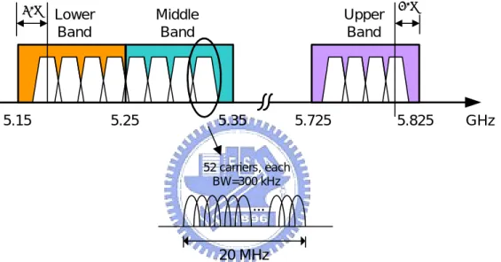
As shown in Fig. 1.2, the IEEE 802.11a standard operates in the 5-GHz unlicensed national information infrastructure (U-NII) band [1]. It provides a total bandwidth of 300 MHz which is nearly four times to the 802.11b. The lower and middle U-NII sub-bands accommodate eight channels in a total bandwidth of 200MHz. The upper U-NII band accommodates four channels in a 100MHz bandwidth. The centers of the outmost channel shall be at distance of 30MHz
S
S
y
y
n
n
t
t
h
h
e
e
s
s
i
i
z
z
e
e
r
r
R RXXA/D
D/A
Inter
-face
P PAA TTXXfrom the band’s edges for the lower and middle U-NII bands, and 20MHz for the upper U-NII band. The standard supports channel bandwidths of 20MHz, with each channel being OFDM modulated signal consisting of 52 subcarrries. Each of the subcarrier can be a BPSK, QPSK, 16-QAM, or 64-QAM modulated signal.
... 20 MHz 52 carriers, each BW=300 kHz GHz 5.15 5.25 5.35 5.725 5.825 Lower Band Middle Band Upper Band 30M 20M
Fig. 1.2 Frequency cannel plan for 802.11a
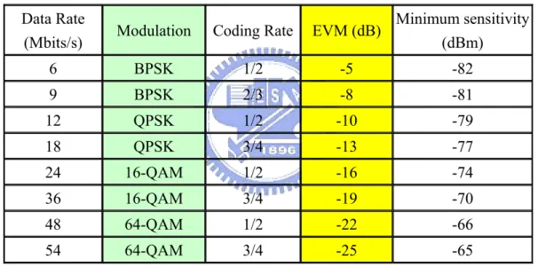
The error vector magnitude (EVM) is used to indicate the quality of digitally modulated signal. EVM takes into account signal impairments such as phase and amplitude mismatches, phase noise, thermal noise and nonlinearity, etc. The modulation schemes and EVM requirements for transmitter are summarized in Table 1.1.
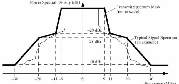
adjacent channel or other wireless applications, IEEE 802.11a regulates maximum power level and transmit spectrum mask. The maximum allowable output power according to FCC regulations is illustrated in Table 1.2. The transmitted spectral density of the transmitted signal shall fall within the spectrum mask, as displayed in Fig. 1.3.
Table 1.1 Modulation scheme and EVM requirement Data Rate
(Mbits/s) Modulation Coding Rate EVM (dB)
Minimum sensitivity (dBm) 6 BPSK 1/2 -5 -82 9 BPSK 2/3 -8 -81 12 QPSK 1/2 -10 -79 18 QPSK 3/4 -13 -77 24 16-QAM 1/2 -16 -74 36 16-QAM 3/4 -19 -70 48 64-QAM 1/2 -22 -66 54 64-QAM 3/4 -25 -65
Table 1.2 Transmit maximum power levels
Frequency band (GHz) Maximum output power with up to 6dBi antenna gain (mW)
5.15~5.25 40 (2.5 mW/MHz)
5.25~5.35 200 (12.5mW/MHz)
Chap 2.
Transmitter Architecture
The purpose of the wireless transmitter is to convey information to radio interface by modulation and up-conversion. The architecture plays an import role in the complexity and performance of the overall transmitter. The transmitter architectures are found in only a few forms, because those issues such as noise, interference rejection, and band selectivity are more relaxed in transmitter than in receivers [2]. In this chapter, we will introduce two types of transmitter
architectures, whose advantages and drawbacks will be discussed in detail.
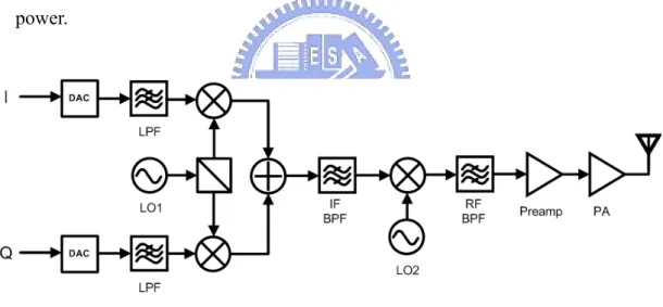
2.1 Superhetrodyne transmitter
Fig. 2.1 shows a traditional superhetrodyne architecture of transmitter. The transmitter up-converts baseband I and Q signal to RF using a carrier generated by mixing the outputs of two local oscillators, LO1and LO2. The first BPF rejects the harmonics of IF signal, while the second BPF remove unwanted sideband of RF signal.
frequencies of the VCO, no injection pulling occurs. Another advantage of superhetrodyne transmitter is better I and Q matching because quadrature
modulation is performed at lower frequencies, leading to less cross-talk between the two bit streams. Moreover, it is easier to control output power in a
superhetrodyne transmitter than in direct conversion.
The transmitter suffers form a number of drawbacks as follows. First, The IF band-pass filter and RF band-pass filter are bulky and expensive. Next, the circuits of the superhetrodyne transmitter are more complex. Therefore it consumes higher power.
Fig. 2.1 Superhetrodyne transmitter
2.2 Direct-conversion transmitter
The direct-conversion transmitter only performs a single frequency conversion to RF as illustrated in Fig. 2.2. In this case, modulation and up-conversion occur in the same circuit. The direct-conversion transmitter is
usually preferred in a fully integrated design, because it avoids the need for an off-chip IF filter and demands only a single frequency synthesizer.
Fig. 2.2 Direct-conversion transmitter
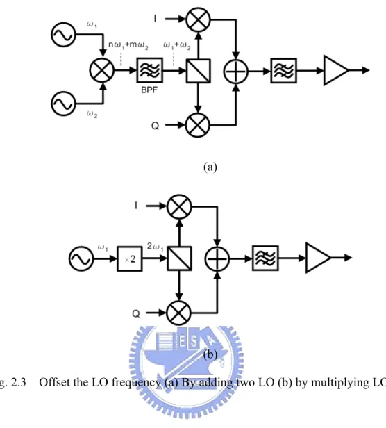
The architecture of Fig. 2.2 suffers from an important drawback: local
pulling or injection pulling. This issue arises because the PA output is a modulated waveform with high power and a spectrum centered around the LO frequency. If the high power signals feedback to the local oscillator through coupling or radiation, it becomes the noise injection to the oscillator. The problem worsens if the PA is turned on and off periodically to save power.
The phenomenon of LO pulling is alleviated if the PA output frequency is sufficiently higher or lower than the oscillator frequency. For quadrature
modulation scheme, this can be accomplished by “offsetting the LO frequency” as shown in Fig. 2.3(a)(b).
(a)
(b)
Fig. 2.3 Offset the LO frequency (a) By adding two LO (b) by multiplying LO
Other issues of direct-conversion transmitter are not as critical as mentioned in the above discussion. First, the power control allocated at RF is harder to maintain accuracy and consumes more power. Second, the quadrature modulation occurs at RF frequency, thus I and Q matching become worse.
Chap 3.
Circuit Implementation
3.1 Circuit block diagram
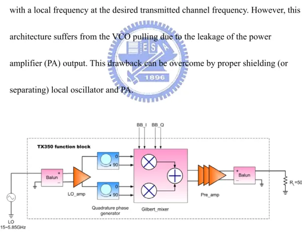
Fig 3.1 shows a block diagram of the transmitter front-end using direct conversion architecture, the modulated I/Q baseband (BB) signal is directly mixed with a local frequency at the desired transmitted channel frequency. However, this architecture suffers from the VCO pulling due to the leakage of the power
amplifier (PA) output. This drawback can be overcome by proper shielding (or separating) local oscillator and PA.
Fig 3.1 Block diagram of the transmitter front-end
In order to reduce size and cost of the transmitter, how to achieve a higher degree of integration of RF circuitry is one of the key design issues. The
transmitter front-end is comprised of two baluns, a local driver amplifier, two quadrature phase generators, an I/Q quadrature modulator (Gilbert cell mixer) and a three-stage pre-amplifier. The I/Q modulator take differential base-band input BB_I and BB_Q, frequency up-converts with the quadrature LO signals, and sums the output signals. On-chip inductors are used as loads at the mixer output to increase the voltage swing. The pre-amplifier boosts the output power to a level capable of driving the external power amplifier.
Precise quadrature LO signals are important for the direct conversion architecture. Any amplitude mismatches or phase differences apart from 90o
between LO_I and LO_Q causes degradation in the error vector magnitude (EVM). This design contains quadrature phase generators to reduce the amplitude mismatch and phase error. The purpose of LO amplifier is twofold: to improve the isolation between the mixer and LO, therefore reducing injection pulling of the LO, and to provide large LO level to optimize the mixer linearity and noise performance.
3.2 Specification
The 802.11a standard provides a total bandwidth of 300MHz in the 5GHz UNII band (5.15 to 5.825GHz), so operating in the 5 to 6 GHz which covers all the UNII frequency bands is our design goal [1]. The maximum allowed transmit
power is 16, 23, and 29dBm, respectively, for channels residing in the lower, middle and upper band. The specification of middle band is chosen in our design. Thus, the maximum output power through antenna is
Pantenna_out,max =23dBm
which contains a 6-dB antenna gain. Hence, the final transmit power before antenna should be below
PTX_OUT,max =23−6=17dBm
The transmitter output power is thus determined as 16dBm with 1-dB margin. Notice that this value is the average output power. The peak-to-average power ratio (PAPR) is the problem to be concerned for OFDM system. In the worst case, suppose 52 peaks for the sinewaves add together, the PAPR will be 10log(52) ≈ 17dB. However, in practice, The PAPR is as low as 6 dB may meet the EVM and packet error rate (PER) requirement of the IEEE 802.11a specifications. Thus, the peak output power is
dBm 22 6 16 , , = + = + =P PAPR
Pout peak outavg
With the Pout and gain of each stage, the output power of each module is
obtained in Table 3.1. In general, the OP-1dB is the maximum operation boundary. After calculation, the OP-1dB of preamp and quadrature mixer are 4dBm and -11dBm, respectively. The relationship between OP-1dB and OIP3 can be
obtained dB 10 3 1 ≈− − OIP dB P O A A (3.1)
The link budget of the entire transmitter system is listed in Table 3.1 and the specifications of transmitter front-end are summarized in Table 3.2.
Table 3.1 Link budget of the entire transmitter
Parameters BPF1 T/R PA BPF2 Pre Amp Mixer LPF DAC Unit
Gain -1 -2 22 -1 15 -5 -2 dB
Pout,avg 14 15 17 -3 -2 -17 -12 -10 dBm
Pout,peak 22 24 25 3 4 -13 dBm
OP-1dB 22 24 25 4 -11 dBm
OIP3 35 14 -1 dBm
Table 3.2 Specifications of the transmitter front-end Parameters Specifications Frequency Range 5-6 GHz Conversion Gain 10 dB IIP3 4 dBm OIP3 14 dBm OP1dB 4 dBm Sideband rejection >30 dB Carrier rejection >30 dB
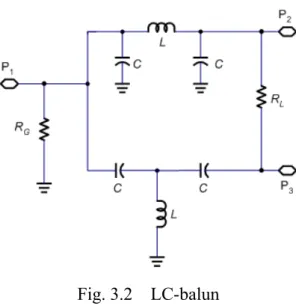
3.3 Balun design
With today’s CMOS IC technology, it can provide high frequency active devices for RF applications, but high quality passive components (e.g., inductors and transformer) present serious challenges for integration. Although significant progress toward the integration of high quality inductors has been reported, practical planar monolithic inductors achieves only moderate performance due to resistive losses in the metal traces and in the underlying substrate.
In this section, two types of baluns (balance to unbalance) which are suitable for CMOS implementation are described. A monolithic transformer comprising two coupled inductors occupies less area and exhibits a higher quality factor (Q) than LC-balun in differential circuits. However, modeling and parameter
extraction of monolithic transformer is more difficult than the other. It also needs 3D electromagnetic simulator and spends much more time on simulation.
On-chip LC-balun is shown in Fig. 3.2. It is easy to be designed and fabricated in IC processes. Therefore, the LC-balun is used in our chip. The insertion loss of the LC-balun is higher
than the monolithic transformer and need carefully design.
We will analyze this circuit by reducing it into two simple half-circuits driven by symmetric source, and redrew the
circuit as shown in Fig. 3.3. Note that the port impedances differ from Fig. 3.2.
(RG’ = 2RG , and RL’ = 1/2RL )
Fig. 3.3
To derive formulas for determining L and C value, let XL = XC and the input
impedance Zin , seen at port 3 toward the port 1, equals RL’
and (3.2) ' ' R // ) ' ( L G C L C L C G in R X X jX jX jX R Z = = − − = Thus XL = RG'⋅RL' = RG⋅RL (3.3)
The balun is designed for the band around 5.5GHz. The frequency response of LC-balun is illustrated in Fig. 3.4, indicating that the phase error between port 2 and port 3 is less than 1.5o and the amplitude mismatch is less than 0.5 dB.
m2 freq= dB(S(2,1))-dB(S(3,1))=-0.3595.500GHz 5.2 5.4 5.6 5.8 5.0 6.0 -0.4 -0.2 0.0 -0.6 0.2 freq, GHz d B (S (2 ,1 ))-d B (S (3 ,1 )) m2 m1 freq= phase(S(2,1))-phase(S(3,1))=179.3615.500GHz 5.2 5.4 5.6 5.8 5.0 6.0 179.5 180.0 180.5 181.0 179.0 181.5 freq, GHz p h a se (S (2 ,1 ))-p h a se (S (3 ,1 )) m1
Fig 3.4 Frequency response of LC- balun
3.4 Quadrature generation design
Quadrature signals can be generated from a local oscillator in several different ways. The most common is the RC-CR
network as shown in Fig. 3.5 [2].
Consider a sinusoidal with frequency ω applied at the input Vin , the outputs Vout1 and
Vout2 is Fig.3.5 RC-CR network RC j V Vout in ω + = 1 1 * 1 (3.4) RC j RC j V Vout in ω ω + = 1 * 2 (3.5)
and hence 2 ) ( tan ) ( tan 2 ) ( 1 1 1 2 π ω ω π = + − = − − − RC RC V V
Ang out out
(3.6)
Thus, Vout1 and Vout2 have 90o phase difference at all frequencies, but the
output amplitudes are equal only at ω = 1/(RC). Usually, it is difficult to achieve the accurate value of on-chip passive components and therefore amplitude
mismatches arise. The amplitude mismatch, which is sensitive to variations in RC value, can be suppressed by limiting amplifiers.
Note that capacitive paths between the two outputs introduce phase error, demanding careful layout. Amplitude mismatches between the load capacitance also contribute to phase error.
Another issue in the circuit of Fig. 3.5 is the harmonic component of Vin .
Suppose Vin = A1cos ωt + An cos nωt, and therefore
[
]
[
2 tan (2 )]
cos 1 4 ) ( tan cos 1 1 2 2 2 2 1 2 2 2 1 1 ω ω ω ω ω ω RC t C R A RC t C R A Vout − − − + + − + = (3.7) ⎥⎦ ⎤ ⎢⎣ ⎡ − + + + ⎥⎦ ⎤ ⎢⎣ ⎡ − + + = − − 2 ) 2 ( tan 2 cos 1 4 2 2 ) ( tan cos 1 1 2 2 2 2 1 2 2 2 1 2 π ω ω ω ω π ω ω ω ω RC t C R RC A RC t C R RC A Vout (3.8)) 2 tan 2 cos( 5 ) 4 cos( 2 1 2 1 1 − − + − = A t A t Vout ω π ω (3.9) ) 2 2 tan 2 cos( 5 ) 4 cos( 2 1 2 1 1 π ω π ω + + − + = − t A t A Vout (3.10)
The result indicates that it has a phase imbalance between Vout1 and Vout2.
Moreover, the magnitude of the harmonics also experiences unequal gains through the two paths, introducing amplitude mismatches at the output. If the LO
harmonics are significant, the RC-CR network must be preceded by a lowpass filter.
The simulation results of RC-CR network are shown in Fig. 3.6, showing that the phase error is less than 0.5o and the mismatch is less than 1 dB between 5 and
6GHz. m1 freq= phase(S(2,1))-phase(S(3,1))=-89.7285.500GHz 5.2 5.4 5.6 5.8 5.0 6.0 -89.74 -89.73 -89.72 -89.75 -89.71 freq, GHz p h a se( S (2 ,1 )) -ph as e (S (3, 1) ) m1 m2 freq= dB(S(2,1))-dB(S(3,1))=-0.0715.500GHz 5.2 5.4 5.6 5.8 5.0 6.0 -0.5 0.0 0.5 -1.0 1.0 freq, GHz d B (S (2 ,1 ))-d B (S (3 ,1 )) m2
3.5 Mixer design
Mixers perform frequency translation by multiplying two signals (and their harmonics). Up-conversion mixers employed in the transmit path have two
distinctly inputs, called the base-band (BB) port and the local oscillator (LO ) port. Several up-conversion mixer topologies that can be realized in CMOS IC
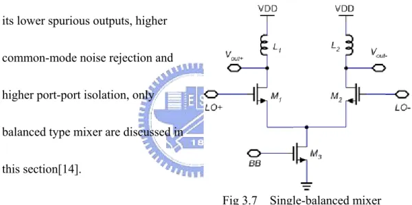
processes are presented. Since balanced mixer designs are more desirable due to its lower spurious outputs, higher
common-mode noise rejection and higher port-port isolation, only balanced type mixer are discussed in this section[14].
Fig 3.7 Single-balanced mixer The single-balanced mixer shown in Fig. 3.7 is the simplest approach that can be implemented in most IC processes. The single balance mixer offers a desired single-ended RF input and it does not require a balun at the input. However, the drawback of single-balance mixer has low 1db compression point, low port-to-port isolation, low IIP3 and high input impedance.
If higher noise figure can be tolerated such as transmitter, the micro-mixer in Fig. 3.8 offers the best IIP3 due to its third-order harmonic distortion cancellation
mechanism. With proper biasing, the input impedance can be set close to 50 ohms which eliminates external matching network. However, using this topology, it would be difficult to increase the gain or reduce the noise figure. It achieves
reasonable port-to-port isolation and eliminates the balun by using a current mirror. Because having three transistors in stack, limits the maximum signal swing and result in a lower output 1-dB compression point.
Fig.3.8 Micro-mixer
The Gilbert cell (double-balanced) mixer was invented in the 60’s, but it still remains to be the most popular mixer circuit. A basic mixer circuit is shown in Fig. 3.9. Baseband (BB) signal is applied to the lower terminals of the stack, and LO
signal is connected to the upper ones. Thus RF signal is obtained as an output. It can prove high conversion gain and high port-to-to isolation. The linearity is reasonably good. Typically, the RF filter preceding this mixer is single-ended so a balun is needed to convert the single-ended signal to differential signal. However, balun having low insertion loss is very difficult to implement in IC processes.
Fig. 3.9 Gilbert cell mixer
The distortion in RF signal is dominated by the lower BB differential pair rather than the upper LO differential pairs. This is because the BB signal is not a single tone signal [13]. Thus, harmonic distortions in the lower differential pair will cause intermodulation distortion, and these intermodulated components may appear at the same frequency of a wanted channel. This intermodulation distortion can be suppressed by improving the linearity of the mixer itself. Hence linearity is
an important parameter for the evaluation of a mixer performance, and it is usually indicated by 1 dB compression point and third-order intercept pointer (IP3).
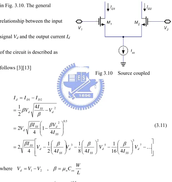
The lower differential pair, called source coupled differential pair, is redrawn in Fig. 3.10. The general
relationship between the input signal Vd and the output current Id
of the circuit is described as follows [3][13]
Fig 3.10 Source coupled
⎥ ⎥ ⎦ ⎤ ⎢ ⎢ ⎣ ⎡ − ⎟⎟ ⎠ ⎞ ⎜⎜ ⎝ ⎛ − ⎟⎟ ⎠ ⎞ ⎜⎜ ⎝ ⎛ − ⎟⎟ ⎠ ⎞ ⎜⎜ ⎝ ⎛ − = ⎟ ⎟ ⎠ ⎞ ⎜ ⎜ ⎝ ⎛ − = − = − = K 7 3 5 2 3 5 . 0 2 2 2 1 4 16 1 4 8 1 4 2 1 4 2 4 1 4 2 4 2 1 d SS d SS d SS d SS SS d SS d d SS d D D d V I V I V I V I I V I V V I V I I I β β β β β β β β (3.11) where L W C V V Vd = 1 − 2 , β =µn ox
The first order term in Eq. (3.11) is a desired component, which is called a fundamental in general. The rest higher order term (V
(
ISS)
Vd 5 . 0 4 / β d3, Vd5,Vd7, …), on the other hand , are distortion components that are not desirable and
coupled pair increases, if tail current source ISS increases. Because the effect is
slight, other linearization techniques have been developed.
A differential pair can be degenerated as shown in Figs 3.11 (a) and (b) [3]. In Fig. 3.11 (a), ISS flows through the degeneration resistors, thereby consuming
voltage headroom of ISSRS / 2. The circuit of Fig. 3.11 (b), on the other hand, does
not involve this issue but it suffers from a slightly higher noise and offset voltage because the two tail current sources introduce some differential error and noise.
Fig. 3.11 Source degeneration applied to a differential pair
Resistive degeneration requires accuracy resistors, which is unavailable in today’s IC technologies. As depicted in Fig.3.13, the resistor can be replaced by a NMOS operating in deep triode region. Recall the I-V relationship of the NMOS in triode region
(
)
⎥⎦⎤ ⎢⎣ ⎡ − − = 2 2 1 DS DS t GS ox n D V V V V L W C I µ (3.12)If in Eq. (3.12), VDS << 2(VGS - VTH ), the last term in Eq. (3.12) can be
neglected and equivalent RON is obtained.
(
GS t)
ox n D DS ON V V L W C I V R − = = µ 1 (3.13)However, for large input swings, M3 may experience substantial change in its
on-resistance. The circuit of Fig. 3.13(a) can be further modified as Fig. 3.13(b). As the gate voltage of M1 becomes more positive than the gate voltage of M2 ,
transistor M3 stays in the triode region because VD3 = VG3 - VG1 whereas M4
eventually enter the saturation region because its drain voltage rises and its gate and source voltage fall. Thus, the circuit remains relatively linear even if one degeneration device goes into saturation.
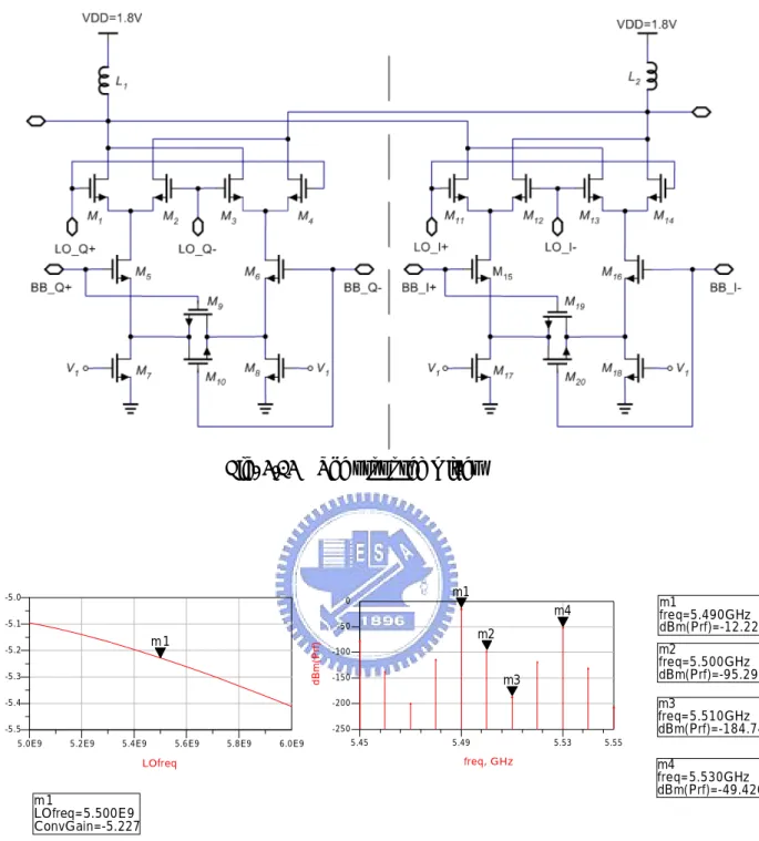
The proposed mixer is illustrated in Fig. 3.13. Because quadrature modulation is required in modern digital communications, the mixer can be divided into two parts: in-phase and quadrature phase part. The in-phase and quadrature phase signal is combined by inductor load at output. The output of the mixer is chosen differential topology because it can eliminate even-order term harmonic distortion and have better common-mode rejection. The output of the mixer is ac-coupled and directly connected to the pre-amplifier input. The matching network of the inter-stage between mixer and preamplifier is not
required because the impedances of mixer output and preamplifier input are close to conjugate match.
Fig. 3.14 and Fig. 3.15 show the performance of the proposed mixer. It achieves a -5.2dB conversion gain at 5.5GHz with 37.2 dB third-order harmonic rejection and the flatness is less than 0.5dB between 5 and 6 GHz. The proposed mixer dissipates 12.6mW which draws 7mA from 1.8V power supply.
Fig. 3.13 The proposed mixer
Fig 3.14 Frequency response Fig 3.15 Harmonic
m1 freq= dBm(Prf)=-12.2275.490GHz m2 freq= dBm(Prf)=-95.2935.500GHz m3 freq= dBm(Prf)=-184.7405.510GHz m4 freq= dBm(Prf)=-49.4265.530GHz 5.49 5.53 5.45 5.55 -200 -150 -100 -50 -250 0 freq, GHz dBm (Pr f) m1 m2 m3 m4 m1 LOfreq= ConvGain=-5.2275.500E9
5.2E9 5.4E9 5.6E9 5.8E9
5.0E9 6.0E9 -5.4 -5.3 -5.2 -5.1 -5.5 -5.0 LOfreq C onv G ai n m1
3.6 Pre-amplifier design
The pre-amplifier is used to boost the output power and to drive external high power amplifier. The proposed pre-amplifier, which consists of a three-stage differential amplifier, is shown in Fig. 3.23. For simplifying analysis, each stage will be discussed individually as follows.
3.6.1 First stage amplifier
The first stage amplifier is shown in Fig. 3.16. The circuit topology is full symmetric, so the half-circuit concept is used for simplifying analysis. Fig. 3.17 shows the equivalent half-circuit of Fig.3.16. It is called the cascode amplifier with single tuned load[5]. The cascode amplifier with tuned load provides selective amplification of
wanted signals and a d of degradation of unwante signals. The use of inductor L
egree d
es lso
1 and L4 not only increas
the headroom but a
cancels the parasitic drain- source and gate-source
capacitance. We can resonate out this capacitance with an appropriate choice of inductance and obtain a maximum gain at arbitrary frequency ω0. The casc
topology (M
ode
1 /M2, M11 /M12) eliminates the Miller effect and improves the
amplifier reverse isolation. The NMOS M3 / M13 operate in deep triode region and
its equivalent resistance RON is obtained by Eq.(3.13).
Fig 3.17 Equivalent half circuit of Fig. 3.16
ω
1ω
0ω
20 dB -3 dB
ω
dB
Fig. 3.18 Frequency response of LC tank For LC tank, the plot
of magnitude function with frequency is shown in Fig. 3.18. The peak magnitude response occurs at the resonant frequency e eC L 1 0 = ω (3.14)
where Le is the parallel inductor, Ce is the parasitic capacitance. The -3dB
e e b R C 1 1 2 − = =ω ω ω (3.15)
where Re is the parallel resistance in LC tank. Assuming RON3 << Re ,
we obtain [3]
(
m1 mb1)
m2 o2( o1// e) at ω0v g g g r r R
A ≈ + (3.16)
It must be noted that Eq.(3.16) is certainly true only at low frequencies. At RF/microwave frequencies, the scattering (S) parameters, which are related to incident and reflected power, are more suitable to describe the two-port network.
This simplified schematic of a single stage amplifier is shown in Fig. 3.19. We can define the transducer power gain GT, which quantifiers the gain of the
amplifier placed between source and load [4].
(
) (
)
(
)(
)
2 12 21 22 11 2 2 21 2 1 1 1 Γ 1 source the from power Available load the to delivered Power L S L S S L A L T S S S S S P P G Γ Γ − Γ − Γ − Γ − − = = = (3.17)For amplifier designer, how to decide the reflection coefficients is an important issue. As examples, in a design requiring maximum transducer power gain, the reflection coefficients are selected as follows [7]
0) ( design unilateral for , 0) ( design bilateral for , 12 * 22 * 11 12 * * = = Γ = Γ ≠ Γ = Γ Γ = Γ S S S S L S ML L MS S (3.18)
where Γ ,MS ΓML are called simultaneous conjugate match.
21 12 22 11 * 11 22 2 * 22 11 1 2 2 11 2 22 2 2 2 22 2 11 1 2 2 2 2 2 1 1 2 1 1 , , 1 , 1 2 4 , 2 4 S S S S S S C S S C S S B S S B C C B B C C B B ML MS − = ∆ ∆ − = ∆ − = ∆ − − + = ∆ − − + = − ± = Γ − ± = Γ (3.19)
In a high power amplifier design, the reflection coefficients are selected as follows
OP L =Γ
Γ (3.20)
where ΓOP is the load reflection coefficients of maximum power.
In a low-noise design, the reflection coefficients are selected as follows
opt S =Γ
Γ (3.21)
where Γopt is the optimum noise reflection coefficients.
In a wideband amplifier design, it is usually necessary to reduce the
gain-bandwidth constrains associated with the impedance to be matched by using resistive feedback or by loading the device with shut or series resistance [4][6]. To
design a wideband amplifier, two different design approaches are used: frequency compensated matching network and negative feedback. Frequency compensated matching network introduce an impedance mismatch to compensate for the
frequency variation. Negative feedback allows a flat gain response and reduces the input and output VSWR over a wide frequency range. In our design, we sacrifice the impedance matching to get wider bandwidth. We also utilize negative
feedback approach, for example, M3 / M13 contributes a series feedback.
3.6.2 Second stage amplifier
The second stage amplifier, shown in Fig. 3.20, shares the same circuit topology as the first stage amplifier but remove two cascade NMOS. It can allow higher signal swing. As mentioned above, the circuit analysis is similar to the first stage amplifier.
3.6.3 Last stage amplifier
The last stage amplifier, serve as a power amplifier, is illustrated in Fig. 3.21. In order to increase the amplifier efficiency, the last stage operates in Class AB mode whose conduction angle is less than 180o. This circuit, is called a push-pull
amplifier, consists of four NMOS devices (M6 /M7, M16 /M17) to share the load
current. The inductors (L3 /L6) play the role of a RF choke providing DC biasing.
The trace width of inductors must be wide enough to support large current density. Fig. 3.21 puts a balun transformer together and redraws the circuit as shown in Fig. 3.22.
Fig. 3.22 Equivalent circuit of Fig. 3.21
The theoretical efficiency for true Class B operation with sinusoidal signals is 78.5%, which is greater than the 50% theoretical maximum obtainable with Class A operation. Although efficiencies near the theoretical limits are obtainable at low frequencies, it is difficult to achieve more than 50% efficiency at
microwave frequencies. There are few Class B amplifiers in the microwave region proposed. This was due the fact that when an MOSFET is biased near pinch-off region, its gain is substantially less than when it is operated at maximum gain point. The efficiency and linearity of Class AB amplifier are intermediate between those of a Class A and Class B amplifiers.
3.6.4 Proposed pre-amplifier
The proposed pre-amplifier employs a fully differential three-stage amplifier as shown in Fig. 3.23. The fully
differential topology has several advantages as follows: lower substrate noise and sensitivity, doubled signal swing, and linearization of transfer function
(elimination the even harmonics). The cost will be higher power consumption. A three-stage amplifier offers sufficient gain and large bandwidth.
Fig 3.24 demonstrates the frequency response of the proposed pre-amplifier. It achieves 20 dB transducer power gain at 5.5 GHz. Notice that the transducer power gain in upper bands is designed higher to compensate the frequency variation of a up-conversion mixer.
m1 RFfreq=
dB(S(2,1))=20.0225.500E9
5.2E9 5.4E9 5.6E9 5.8E9
5.0E9 6.0E9 16 17 18 19 20 15 21 m1 RFfreq dB (S (2 ,1 ))
Fig 3.24 Frequency response of the proposed pre-amplifier
3.7 Simulation results
The simulation results of the entire transmitter front-end are shown in this section. Fig.3.25 exhibits the harmonics of in-band spectrum at 5.5GHz. This diagram tells us that sideband rejection is 38.7dB, carrier rejection is 33.4dB and three-order harmonic rejection is 36.9dB. Fig.3.26 and Fig. 3.27 show the in-band spectrum at 5GHz and 6GHz respectively. The harmonics of out-of-band spectrum are shown in Fig 3.28. Indicating that it achieves 23.2dB out-band rejection.
Fig. 3.29 and 3.30 illustrates the frequency response of the conversion gain and the output power, respectively. As the figure indicates, the conversion gain equals 13.8 dB at 5.5GHz, and the flatness is less than 3 dB over the entire band. Fig. 3.31 and 3.32 shows the output P1dB, IIP3 and OIP3 which are 10.5dBm, 5dBm and 15dBm, respectively. The entire transmitter front-end dissipates 54mW
which draws 30mA from 1.8V power supply. m1 freq= dBm(Prf)=6.8895.490GHz m2 freq= dBm(Prf)=-26.5485.500GHz m3 freq= dBm(Prf)=-31.8685.510GHz m4 freq= dBm(Prf)=-30.1275.530GHz 5.45 5.55 -50 50 -150 100 freq, GHz dB m (P rf) m1 m2 m3 m4
Fig. 3.25 Harmonics of in-band spectrum at 5.5GHz
m1 freq= dBm(Prf)=4.1494.990GHz m2 freq= dBm(Prf)=-27.8385.000GHz m3 freq= dBm(Prf)=-19.2355.010GHz m4 freq= dBm(Prf)=-34.4115.030GHz 4.95 5.05 -50 50 -150 100 freq, GHz dB m (P rf) m1 m2 m3 m4
Fig. 3.26 Harmonics of in-band spectrum at 5GHz
m1 freq= dBm(Prf)=5.2835.990GHz m2 freq= dBm(Prf)=-28.1636.000GHz m3 freq= dBm(Prf)=-28.7716.010GHz m4 freq= dBm(Prf)=-31.8826.030GHz 5.95 6.05 -50 50 -150 100 freq, GHz dB m (P rf) m1 m2 m3 m4
m5 freq= dBm(Prf)=6.8895.490GHz m6 freq= dBm(Prf)=-16.33110.98GHz 2 4 6 8 10 12 14 16 0 18 -200 -150 -100 -50 0 -250 50 m5 m6 freq, GHz dB m (P rf)
Fig. 3.28 Harmonics of out-band spectrum
m1 LOfreq= ConvGain=13.8895.500E9 m2 LOfreq= ConvGain=11.1495.000E9 m3 LOfreq= ConvGain=12.2836.000E9
5.2E9 5.4E9 5.6E9 5.8E9
5.0E9 6.0E9 11.5 12.0 12.5 13.0 13.5 11.0 14.0 LOfreq C onv G ain m1 m2 m3
Fig 3.29 Frequency response of the conversion gain
m4 LOfreq= P11m_Tone=4.145.000E9 m5 LOfreq= P11m_Tone=6.885.500E9 m6 LOfreq= P11m_Tone=5.286.000E9
5.2E9 5.4E9 5.6E9 5.8E9
5.0E9 6.0E9 4.5 5.0 5.5 6.0 6.5 4.0 7.0 LOfreq P 11 m _T on e m4 m5 m6
m1 Power_BB= P11m_Tone=10.518-4.000 m2 Power_BB= Power_linear=11.330-4.000 -18 -16 -14 -12 -10 -8 -6 -4 -2 -20 0 -5 0 5 10 15 -10 20 Power_BB P 11m _T on e m1 P o we r_ lin e a r m2
Fig 3.31 Ouput-1dB compression point
-1 8 -16 -14 -12 -10 -8 -6 -4 -2 0 2 4 6 8 10 12 14 16 18 -2 0 20 -30 -20 -10 0 10 20 30 -40 40 Power_BB P rf T on e P 13 m _T one P 13 p_T on e
Fig 3.32 Input IP3 and Output IP3 point
3.8 Other applications
In this section, we utilize the same architecture of the transmitter, but change and optimize the component values for dual band and ultra-wide band applications.
3.8.1 Dual band (2.4GHz)
Fig.3.33 exhibits the harmonic of in-band spectrum at 2.45GHz. The sideband rejection is 7.8dB, carrier rejection is 38.7dB, three-order harmonic rejection is 45.3dB and the conversion gain is 10.2dB. The harmonic of out-band spectrum is shown in Fig 3.34. It reaches an 8.6dB out-band rejection.
m1 freq= dBm(Prf)=3.5892.440GHz m2 freq= dBm(Prf)=-35.2672.450GHz m3 freq= dBm(Prf)=-4.3162.460GHz m4 freq= dBm(Prf)=-41.8302.470GHz 2.43 2.48 -150 -100 -50 0 -200 50 freq, GHz dB m (P rf ) m1 m2 m3 m4
Fig 3.33 Harmonics of in-band spectrum at 2.45GHz
m5 freq= dBm(Prf)=3.5892.440GHz m6 freq= dBm(Prf)=-5.1064.880GHz 1 2 3 4 5 6 7 0 8 -150 -100 -50 0 -200 50 m5 m6 freq, GHz dB m (P rf )
3.8.2 UWB Band (10GHz)
The harmonic of in-band spectrum at 9.5GHz is shown in Fig. 3.35. As the diagram indicates that sideband rejection is 37.2dB, carrier rejection is 30.7dB, three-order harmonic rejection is 35.7dB and the conversion gain is 6.1dB. Fig 3.36 shows the harmonic of out-band spectrum. It achieves a 32.9dB out-band rejection. m1 freq= dBm(Prf)=-0.9899.490GHz m2 freq= dBm(Prf)=-31.7529.500GHz m3 freq= dBm(Prf)=-38.2249.510GHz m4 freq= dBm(Prf)=-36.7089.530GHz 9.52 9.42 9.58 -100 0 freq, GHz dB m (P rf ) m1 m2 m3 m4
Fig 3.35 Harmonics of in-band spectrum
m5 freq= dBm(Prf)=-0.9899.490GHz m6 freq= dBm(Prf)=-34.94118.98GHz 5 10 15 20 25 0 30 -250 -200 -150 -100 -50 -300 0 m5 m6 freq, GHz dB m (P rf )
Chap 4.
Layout Considerations
4.1 Chip layout considerations
Someone said that making a layout is an art by itself. Some layouters claim that they have made a good layout when the layout-versus-schematic (LVS) check shows no error messages. This is a necessary, but not sufficient condition for a good RF layout. Poor layout causes the performance degradation of the circuits, or even result in wrong working. There are some design rules helping us to make a better layout, as follows.
First of all, in order to avoid the phenomenon of LO pulling, the RF output stage (PA) should be physically far away from the LO circuits. But it is difficult to do that in our chip. To minimize the effect, RF output stage and LO circuits are placed perpendicularly to each other. In IC processes, “guard rings” can also be employed to reduce the coupling.
Next, the fully differential topology is used in our design, the mismatch and symmetry should be concern. The common-centroid configuration is employed to
reduce device mismatch due to the effect of gradient. Moreover, the trace length of the connections for each stage must keep as equal as possible to minimize phase error.
Finally, how to determine the trace width of those connections is an
important issue. For DC paths, it should be wide enough to support large current. For RF paths, the parasitic capacitor will be increased, if we increase the trace width. However, narrow trace raises parasitic inductor and the metal resistor. To solve this problem, we will introduce a transmission concept. For a lossless transmission line, the characteristic impedance is obtained as
C L
Z0 = (4.1)
where L is series inductance per unit length and C is shunt capacitance per unit length. Many CAD tools can provide the characteristic impedance of the planar transmission lines (e.g., coplanar waveguide, microstrip and stripline etc.). Our design employs a 50 Ω microstrip line, which characters are listed as follows: dielectric constant ε = 4.1 (SiO2), the height is 2.1µm. Thus the width of a
microstrip line can be obtained as 4 µm.
Consider the case of a bend in a microstrip line, is illustrated in Fig.4.1. The straightforward right-angle bend has a parasitic discontinuity capacitance. This effect could be minimized by mitering the corner. The optimum value of the miter
length a, depends on the characteristic impedance and the bend angle, but a value of a = 1.8W is often used in practice. The chip layout is shown in Fig. 4.2, and the chip area occupied 2.5×2.5 mm2.
Fig. 4.1 Bend of a microstrip line
4.2 Package and ESD considerations
The 20-pin QFN package provided by SPIL is employed in our design as illustrated in Fig. 4.3. To prevent crosstalk due to adjacent pin coupling, the RF pins (LO and RF_out pin) are surrounded by ground wire, and the LO pins is allocated away from the RF_out pin. Fig 4.4 shows the simplified package model for each pin. Each pin exhibits a finite self-inductance which is about 1-nH. Multiple bond wires and pins are used to decrease the equivalent inductance and resistance on the VDD and ground pins. A large on-chip capacitor, which is
composed of four MIM capacitors in this chip, is used to stabilize the difference between VDD
and ground, and reduce the risk of inter-stage coupling.
Fig. 4.4 Package model for each pin
Electrostatic discharge (ESD) may result in CMOS devices permanent damage without protection circuits. Fig. 4.5 shows the most popular ESD protection circuits in commercial using. The diode chains clamp the external discharge to ground or VDD, and a large gate ground NMOS will break down once
enormous potential across VDD and ground. The ESD protection circuits provided
by UMC ensure 3.6KV in human body mode (HBM) test but induce about 40fF capacitances in each pin. The ESD
parasitic capacitances and the bond-wire inductors must be considered together during simulation.
4.3 PCB layout considerations
The transmitter chip is mounted on the PCB board as shown in Fig. 4.6. The layer stack-up structure of a PCB is illustrated in Fig. 4.7. The loss tangent (δ= 0.0021) and dielectric constant stability for RO4003 material is superior to FR-4, so that RO4003 severs as the dielectric material (εr= 3.38) between layer 1 and
layer 2. As mentioned above, the microstrip characteristic impedance could be obtained by CAD tools (APPCAD 3.0, Agilent), as shown in Fig. 4.8. We obtain the width of transmission line equals 17 mil. Layer 2 and layer 3 provide large and low impedance power planes. The area of the power planes near the chip look like a good, high frequency capacitor and help with decoupling.
The design rules of PCB layout are similar to the chip layout. The RF output port should be put away from the LO port. For differential paths, equal length and symmetric layout is essential. In order to reduce transmission loss, mitering corners on microstrip traces are formed and the microstrip length is as short as possible.
Fig. 4.6 PCB board
Chap 5.
Measurement
Fig.5.1 shows the essential instruments which characters are listed as follows:
Spectrum analyzer (PSA, Agilent E4446A) 3Hz ~44GHz ×1 Signal generator (ESG, Agilent E4438C) 250K~6.0GHz ×2 Signal generator (ESG, Agilent E4432B) 250K~3.0GHz ×2 Power supply (Agilent E3610A) 0~8V 3A, 0~15V 2A ×1
Fig. 5.1 Instrument overview
Supply ESG (250K~ 3G)
PSA
5.1 Harmonic test
5.1.1 Instrument setup
The equipments are connected as shown in the Fig. 5.2, and use the
following procedure to set up those instruments for measuring the harmonics of the transmitter IC. Note that the 10MREF_OUT terminal of ESG1 must be connected to the 10MREF_IN of ESG2.
1. Set up the Spectrum analyzer parameters as follows: Center frequency = 5.5 GHz, Span = 100MHz, Amplitude = 10dBm, RBW = 300 KHz. 2. Set up the ESG1/ESG2 parameters: Frequency = 10MHz, Level =
-7dBm.
3. Because the I and Q channel signals have 90o phase difference, it is necessary to calibrate the phase before the measurement. Using the following steps (4~5) to do that.
4. Adjust the ESG2 Phase until the lower and upper sideband harmonics are equal, as shown in Fig. 5.3. Recode the phase θ1.
5. Assign the ESG2 Phase θ2=θ1-90o.
6. For the ESG3, set up the parameter as follows: Frequency = 5.5GHz,
Fig. 5.2 Instrument configuration for harmonic test
5.1.2 Results
Fig 5.4 exhausts the measured transmitter in-band spectrum when the
10MHz quadrature signals are applied to the input terminals of the BB_I and BBQ. Fig. 5.4 shows that it archives a sideband rejection of 34.3dB, a carrier rejection of 32.4dB and a third-order harmonic rejection of 31.1dB.
The out-of-band spectrum is illustrated in Fig.5.5, and it tells that the out-of-band rejection equal 51.8dB.
Fig. 5.5 Out-of-band spectrum
5.2 Frequency response test
5.2.1 Instrument setup
Connect the equipments as shown in the Fig.5.2, and use the following procedure to set up these instruments for measuring the frequency response.
1. Set up the spectrum analyzer parameters as follows: Center frequency = 5.5 GHz, Span = 1.5GHz, Amplitude =10dBm, RBW = 300KHz,
Trace> Maxhold mode.
2. Set up the ESG1/ESG2 following parameters: Frequency = 10MHz,
ESG2
3. For the ESG3, set the Level = 1.5dBm and sweep Frequency from 5GHz to 6GHz.
5.2.2 Results
The frequency response of the output power is displayed in Fig. 5.6. The flatness remains below 4.1 dB over the entire band. The frequency response of the conversion gain is obtained by a MATLAB program for calculation and plotting as shown in Fig. 5.7. The conversion gain equals 10.5 dB at 5.5GHz. It must be noted that the cable loss (about 1.5dB) must be considered during the calculation.
5 5.1 5.2 5.3 5.4 5.5 5.6 5.7 5.8 5.9 6 7.5 8 8.5 9 9.5 10 10.5 11 11.5 12 frequency (GHz) C onv er s ion gai n ( d B )
Fig. 5.7 Frequency response of conversion gain
5.3 Output P1-dB test
5.3.1 Instrument setup
Connect the equipment as shown in the Fig. 5.2, and use the following procedure to set up those instruments for measuring output 1-dB compression point.
1. Set up the spectrum analyzer parameters as follows: Center frequency = 5.5 GHz, Span = 100MHz, RBW = 300 KHz, Amplitude = 10dBm 2. Set up the ESG1/ESG2 following parameters: Frequency = 10MHz,
Level = -7dBm and the phase difference = 90o between the ESG1 and
ESG2.
3. For the ESG3, set the Frequency = 5.5GHz and sweep Level from -20 to 0dBm.
5.3.2 Results
The measured data are recorded and plotted by MATLAB as shown in Fig.5.8. It indicates that the output 1-dBompressioin point occurs at 3.8dBm when the BB_power of -5dBm is applied.
-20 -18 -16 -14 -12 -10 -8 -6 -4 -2 0 -10 -8 -6 -4 -2 0 2 4 6 8 10 Out put ( d B m ) BB power (dBm) Output P1dB = 3.74dBm Input P1dB = -5dBm P11m linear
Fig. 5.8 OP-1dB compression point
5.4 IIP3 and OIP3 test
5.4.1 Instrument setup
The equipments are connected as shown in the Fig.5.2, and use the following procedure to set up those instruments for measuring IIP3 and OPI3.
5.5 GHz, Span = 100MHz, RBW = 300 KHz, Amplitude = 10dBm 2. Set up the ESG1/ESG2 parameters: Frequency = 10MHz, Level =
-7dBm and the phase difference = 0o between the ESG1 and ESG2. 3. For the ESG3, set the Frequency = 5.5GHz and sweep Level from -20 to
0dBm.
5.4.2 Results
The IIP3 and OIP3 point can be found by a simple MATLAB program. The measured data are recorded and plotted as shown in Fig.5.9. As the figure indicates, the IIP3 and the OIP3 is about 8dBm, 13.4dBm, respectively.
-20 -15 -10 -5 0 -60 -50 -40 -30 -20 -10 0 10 Ou tp u t ( d B m ) BB power (dBm) Output IP3 = 13.4056dBm Input IP3 = 8dBm P11mP13p
5.5 Transmit spectrum mask test
5.5.1 Instrument setup
Connect the equipments as shown in the Fig.5.10. The BB_I/BB_Q port is connected to the I /Q _output connector of ESG1. In order to control the ESG1 for creating an 802.11a OFDM waveform, Agilent Signal Studio software is launched. The Agilent Signal Studio configuration is illustrated in Fig. 5.11. After
downloading the 802.11 OFDM signal to the ESG1 by the LAN or GPIB interface, use the following procedure to set up the spectrum analyzer (PSA) parameters for measuring the spectrum mask.
1. Press MODE > Spectrum analysis. 2. Press Frequency Channel > 5.5 GHz
3. Press Mode Setup > Radio Std > More 1 of 3 > More 2 of 3 > 802.11a,
Measure > More 1 of 2 > Spectrum Emission Mask, and Meas Setup
Fig. 5.10 Instrument configuration for spectrum mask test
5.5.2 Results
Fig. 5.12 displays the measured transmitter output spectrum while transmitting a -7.22dBm 54Mb/s QAM64 modulated signal. Because the PSA power measurement is averaging the power of the bursted transmission, the actual power can be calculated using the following equation
Power = Displayed Total Pwr +10 × log (duty cycle) + cable loss (5.1)
The actual output power is about -4.7dBm, if the duty cycle is 80 %.
5.6 System test
5.6.1 Instrument setup
The MIMO (multiple input multiple output) system can transmit or receive simultaneously two or more path signals by multiple antennas to overcome
multi-path phenomenon. The transmitter chips are verified in the MIMO system as shown in Fig. 5.13. The diagram only shows the connection of path one signal, another path signal is directly connected by a cable. The data rate of entire system is about 40 Kb/s, which is limited by the DSP (base-band processor) performance.
5.6.2 Results
Fig. 5.11 displays the transmitted/received images in the MIMO system. We compare the difference between the transmitted and received images. The antenna 1 images show the path1 signal, which is transmitted by this chip. The antenna 2 images are transmitted in a direct connection. The diagram tells us that the transmitted image differs slightly the received image, and the bit error rate is 2.27×10⁻³.
5.7 Summary
The specifications, simulations and measurements are summarized in Table 5.1. According to Table 5.1, we can find that the major difference between
simulations and measurements is OP 1-dB compression point. We will analyze the reasons of the errors as follows. First, the imperfect chip and PCB layout result in the performance degradation. Second, the circuit model (e.g. NMOS, ESD and package) not accuracy enough, especially operating in large signal swing. It is a great challenge to prove and meliorate that. This chip compares the performance with papers proposed as shown in Table 5.2[15][8] and Table 5.3[10][11][12].
Table 5.1 Performance of summary
Parameters Specifications Simulations Measurements
Power Consumption N/A 54 mW 63 mW
Frequency 5~6 GHz 5~6 GHz 5~6 GHz Conversion Gain 10 dB 13.8 dB 10.5 dB OIP3 14 dBm 15 dBm 13.4 dBm Output P1dB 4 dBm 10.5 dBm 3.8 dBm Flatness N/A 2.7 dB 4.1 dB Sideband rejection >30 dB 38.7 dB 34.3 dB Carrier rejection >30 dB 33.4 dB 32.4 dB
Table 5.2 Performance of comparison
Parameters This work Po-Niang Lin (2003) Ting-Ping Liu(2000)
IC process CMOS 0.18µm CMOS 0.18µm CMOS 0.25µm
Die size 6.25m2 6.25m2 2.7m2 Power Consumption 63 mW 47 mW 120 mW Frequency 5~6 GHz 5.15~5.35GHz NA Conversion Gain 10.5 dB -14.5 dB NA OIP3 13.4 dBm NA NA Output P1dB 3.8 dBm -6.6 dBm -2.5 dBm Flatness 4.1 dB NA NA Sideband rejection 34.3 dB 26 dB 33.4 dB Carrier rejection 32.4 dB 18 dB 22.4 dB
Table 5.3 Performance of comparison
Parameters Zargari(2002) Zhang(2002) Behzad(2003)
IC process CMOS 0.25µm CMOS 0.18µm CMOS 0.18µm
Die size 22m2(Tx/Rx) 22m2(Tx/Rx) 11.7m2(Tx/Rx) Power Consumption 790 mW 135mW 380mW Frequency 5.16~5.34GHz 5.15~5.35GHz 5.15~5.35GHz Conversion Gain NA NA NA OIP3 NA 15dBm NA Output P1dB 17.8dBm 5dBm 19 dBm Flatness NA NA NA Sideband rejection 51 dB 50 dB NA Carrier rejection 29 dB 38 dB NA
Chap 6.
Conclusions
A 5GHz transmitter front-end chip for IEEE 802.11a is implemented and measured. The transmitter IC is fabricated in UMC 0.18-µm 1P6M CMOS technology and packaged in SPIL QFN20. The die occupied 2.5×2.5 mm2. This
chip achieves an output 1-dB compression of 3.8dBm at 5.5GHz with 10.5dB conversion gain and 34.3dB sideband rejection. Although imperfect layout and inaccurate device model causes the degradation of RF performance, it still can work well on system test verification.
References
[1] IEEE Standard 802.11a-1999: Wireless LAN MAC and PHY Specifications -- High-speed Physical Layer in the 5GHz Band, New York, IEEE. 2000.
[2] B. Razavi, RF Microelectronics, New Jersey, Prentice-Hall, 1998.
[3] B. Razavi, Design of Analog CMOS Integrated Circuits, International Edition, New York, McGraw-Hill, 2001.
[4] R. Ludwig, P. Bretchko, RF circuit design, New Jersey, Prentice-Hall, 2000. [5] T. H. Lee, The design of CMOS radio-frequency integrated circuits, New York,
1998
[6] G. D. Vendelin, A.M. Pavio, U. L. Rohde, Microwave circuit design using linear and nonlinear techniques, John Wiley & Sons, 1990
[7] G. Gonzalez, Microwave transistor amplifiers analysis and design, 2nd edition,
New Jersey , Prentice-Hall, 1997
[8] Ting-Ping Liu, Eric Westerwick, “5-GHz CMOS radio transceiver front-end chipset”, IEEE J. Solid-State Circuits, vol. 35, pp.1927-1933, Dec.2000
[9] M. A. Margarit, D. Shih, P. J. Sullivan, F. Ortega, ”A 5-GHz BiCMOS RFIC front-end for IEEE802.11a/HiperLAN wireless LAN”, IEEE J. Solid-State Circuits, vol. 38, pp. 1284-1287, Jul. 2003
[10] M. Zargari, B. A. Wooley, et. al. “A 5-GHz CMOS transceiver for IEEE 802.11a wireless LAN systems,” IEEE J. Solid-State Circuits, vol. 37, pp. 1688-1694, Dec. 2002.
[11] Pengfei Zhang, Thai Nguyen, Chris Lam, Doug Gambetta, et. al. “A direct conversion CMOS transceiver for IEEE 802.11a WLANs”, ISSCC 2003, paper 20.3, 2003
[12] A. R. Behzad, Z. M. Shi, S. B. Anand, Li Lin, K.h A. Carter, et. al. ”A 5GHz direct-conversion CMOS transceiver utilizing automatic frequency control for the IEEE 802.11a wireless LAN standard”, IEEE J. Solid-State Circuits, vol. 38, pp.2209-2220, Dec. 2003
[13] Eunseok Song, Soo-Ik Chae, Wonchan Kim, “A 2GHz CMOS down-converter with robust image rejection performance against the process variations”, Journal of the Korean Physical Society, Vol.35, pp. s918-926, Dec. 1999
[14] Glenn Watanabe, Henry Lau, Juergen Schoepf, “Integrated Mixer design”, Motorola Inc.
[15] Po-Niang Lin, “5GHz CMOS transmitter front-end for IEEE 802.11a”, M.S. Thesis, National Chiao-Tung University, 2003