國 立 交 通 大 學
電子工程學系 電子研究所碩士班
碩 士 論 文
緩衝層與經氫氣回火矽晶圓對具氮化矽覆蓋層之
形變
N 型金氧半場效電晶體之元件特性及可靠度
之影響
Impacts of a Buffer Layer and Hi-wafers on the
Performance of Strained-channel NMOSFETs
with SiN Capping Layer
研 究 生:蔡子儀
指導教授:林鴻志 博士
黃調元 博士
中 華 民 國 九 十 六 年 六 月
緩衝層與經氫氣回火矽晶圓對具氮化矽覆蓋層之
形變
N 型金氧半場效電晶體之元件特性及可靠度
之影響
Impacts of a Buffer Layer and Hi-wafers on the
Performance of Strained-channel NMOSFETs
with SiN Capping Layer
研 究 生:蔡子儀
Student:Tzu-I Tsai
指導教授:林鴻志 博士 Advisors:Dr. Horng-Chih Lin
黃調元 博士
Dr. Tiao-Yuan Huang
國 立 交 通 大 學
電子工程學系 電子研究所碩士班
碩 士 論 文
A Thesis
Submitted to Department of Electronics Engineering & Institute of Electronics College of Electrical and Computer Engineering
National Chiao-Tung University in Partial Fulfillment of the Requirements
for the Degree of Master of Science
in
Electronic Engineering June 2007
Hsinchu, Taiwan, Republic of China
Vita
姓名 : 蔡子儀 性別 : 男 生日 : 72.5.1 出生地 : 台南市 籍貫 : 台灣省 台南市 地址 : 台南市北成路6 巷 3 號 學歷 : 台南市國立台南一中 1998.09~2001.06 國立中興大學 電機工程學系 2001.09~2005.06 國立交通大學 電子工程研究所 2005.09~2007.06 論文題目: 緩衝層與經氫氣回火矽晶圓對具氮化矽覆蓋層之形變N 型金氧半場效 電晶體之元件特性及可靠度之影響Impacts of a Buffer Layer and Hi-wafers on the Performance of Strained-channel NMOSFETs with SiN Capping Layer
緩衝層與經氫氣回火矽晶圓對具氮化矽覆蓋層之
形變
N 型金氧半場效電晶體之元件特性及可靠度
之影響
研究生 : 蔡子儀 指導教授 : 林鴻志 博士
黃調元 博士
國立交通大學
電子工程學系 電子研究所碩士班
摘要
在本研究中,我們探討了使用氮化矽覆蓋層與四乙氧基矽烷(TEOS)氧化矽緩 衝層對具有形變通道的n-型電晶體的性能影響與可靠度分析。元件分別製作於 CZ 晶圓與經氫氣回火矽晶圓(Hi-wafer)。另外,元件通道植入氟離子對電晶體的性能 影響與可靠度分析亦一併討論。實驗結果發現元件製作於 Hi-wafer 上,其四乙氧 基矽烷氧化矽緩衝層對元件不會造成特性的衰退;然而,元件製作於CZ-wafer 上 卻造成特性的衰退,以上的差異是由於 Hi-wafer 的良好表面品質及較少的基板含 氧量。另一方面,氟離子的通道植入對於元件製作於CZ-wafer 上造成特性明顯的 衰退,例如:轉移電導及次臨界斜率,然而採用 Hi-wafer 作為基板並不會產生以 上的負面影響。沉積氮化矽覆蓋層所造成的熱預算使通道中的硼離子再擴散,進 而消除逆短通道效應,但是卻會使多晶矽空乏現象變嚴重。我們發現氫氣是對具 有形變通道元件產生可靠度衰退的主要原因,而四乙氧基矽烷氧化矽緩衝層可有 效阻擋沉積氮化矽覆蓋層所產生的氫氣擴散進入通道及二氧化矽與矽基板間的介 面。當與對照條件做比較時,無論是在CZ 晶圓或是在經氫氣回火矽晶圓,於閘極上方所沉積的氮化矽覆蓋層皆對元件熱電子衰退特性造成不利影響。然而,在沉 積氮化矽覆蓋層前先沉積四乙氧基矽烷氧化矽緩衝層,雖然其熱電子衰退特性比 對照條件差,但明顯地改善元件可靠度。此外,元件通道植入氟離子的確對可靠 度造成明顯的改善。
Impacts of a Buffer Layer and Hi-wafers on the
Performance of Strained-channel NMOSFETs
with SiN Capping Layer
Student : Tzu-I Tsai Advisors: Dr. Horng-Chih Lin
Dr. Tiao-Yuan Huang
Department of Electronics Engineering and Institute of Electronics
National Chiao Tung University, Hsinchu, Taiwan
Abstract
In this thesis, the effects of Si3N4 layer capping and TEOS buffer layer inserted
prior to the Si3N4 deposition on the NMOS device characteristics as well as correlated
hot-electron degradations were investigated. The test devices were fabricated on two kinds of substrates, namely, Cz and Hi-wafers. Besides, the influence of fluorine channel implant on both the fundamental performance and related reliability of the fabricated devices were also explored. For devices fabricated on the Hi-wafer, the presence of buffer layer does not degrade device performance. In contrast, the presence of buffer layer on devices fabricated with Cz wafers does degrade the performance. Such disparity is attributed to the better surface quality of the Hi wafers. On the other hand, the F channel implant significantly impacts the device performance for devices built on Cz wafers, such as degradation of Gm and S.S. When Hi wafers were used as the starting substrates, such negative impacts is relaxed. These findings highlight the merits of Hi wafers over Cz wafers. The thermal budget associated with the deposition
of Si3N4 capping layer helps redistribute the segregated boron dopants in the channel
and alleviate the reverse short-channel effect, albeit with worsened poly-depletion effect. More importantly, we found that hydrogen species is the primary culprit for aggravated reliabilities in strained devices. The TEOS buffer layer could effectively block the diffusion of hydrogen species from Si3N4 into the channel and Si/SiO2 interface during
Si3N4 deposition as well as subsequent thermal cycles. The hot-electron degradation is
adversely affected when the Si3N4 capping layer is deposited over the gate, compared
with the control samples, regardless of the types of starting wafers. When a TEOS buffer layer was inserted prior to the Si3N4 deposition, although still worse than the
control ones, significant improvement in terms of hot-carrier degradation is achieved. Besides, with the assistance of the F channel implant, the hot-carrier degradation of is obviously improved.
Acknowledgement
短短兩年的碩士生涯就這樣過去了,這篇論文能完成,是多虧大家鼎力幫助。 首先要感謝的,是我的指導教授,黃調元博士與林鴻志博士。在兩位教授身 上,我才知道這兩年所學的知識真是微不足道。黃老師在專業領域的淵博知識及 非專業領域的文學造詣,真的令學生由衷敬佩。而林老師不僅提供了正確的元件 物理觀念及製程實務上的經驗,且在研究過程中不時提出特殊見解,真是讓學生 有種天外飛來一筆的感覺,實在獲益良多。由於有兩位指導教授的幫忙與鼓勵, 使得我能順利完成碩士學位,在此以最真誠的心感謝您們。另外還要感謝簡昭欣 博士,在做實驗最苦悶時給我很多好吃的東西,讓我疲累不堪的身體得到足夠養 分繼續衝刺,在此真是謝謝您。 接下來要感謝的是實驗室的學長們,首先是李耀仁學長,感謝學長在實驗上 秉持嚴格態度及量測方面所堅持”量到什麼就是什麼”的原則,深刻地讓我了解什麼 是學術良心。謝謝呂嘉裕學長,無論在製程實務的經驗傳承,還是量測方法的建 立,都間接地指導我,即使學長已畢業了仍不厭其煩地為我一一解答問題。而畢 業已久的盧文泰學長為我們實驗室所架設的量測系統,更是對我有最直接的幫 助,感謝盧文泰學長。接下來要感謝蘇俊榮學長及盧景森學長,不管是基本paper 方面的問題或是製程上的小技巧,皆不厭其煩地為我解答,尤其是蘇俊榮學長在 材料分析方面的幫忙更是讓我感激不盡。李明賢學長在基本觀念及電腦運用上的 傾囊相授,謝謝李明賢學長。還有感謝張凱翔學長、徐行徽學長、黃健銘學長、 謝雨霖學長在實驗及生活上所給予的關懷與鼓勵,尤其是張凱翔學長在我夜深人 靜量測時提供的提神補品更是惠我良多。 除了學長們外,我很高興認識了ㄧ群好戰友,詹凱翔、王偉銘、黃建富、黃 育峯、王子銘、李克慧,同時也是ㄧ同做實驗打拼量測的好伙伴。除了在學業研 究上的討論之外,在日常生活中也帶給我許多歡樂,謝謝你們讓我在碩士班兩年 生涯中留下許多快樂的回憶,友誼長存。另外,我還要感謝 NDL 的陳敬憲、Jeff在量測分析數據上大力幫忙及許多小姐在實驗過程的幫助,沒有你們就沒有這一 份論文,真是感恩啊! 還有女友欣怡,ㄧ路走來始終如一默默在我身邊給予相當的支持與鼓勵,讓 我能保持作實驗及量測的最高動力。最後是我的家人們,父母、姊姊們,你們給 予我的支持,還有不時的關心,也是讓我完成學業的最大功臣。要感謝的人太多, 或許有沒提到的人,但你們在我心中依然佔了重要的位置,在這裡獻上最誠摯的 歉意與最大的感謝,謝謝大家,謝謝。 蔡 子 儀 誌于風城交大 2007
Contents
Vita………...
iAbstract (in Chinese) ...
iiAbstract (in English)..……….
ivAcknowledgment ...
viContents…...
viiiList of Figure Caption...
xChapter 1 Introduction ...
11-1 General Background...
11-1.1 Introduction
...
11-1.2 Strained-Si device physics
...
31-1.3 Hi-wafer technology
...
71-1.4 Hot Carrier Effect
...
81-2 Motivation... 9
1-3 Organization of This Thesis ... 9
Chapter 2 Device Fabrication and Measurement Setup
...
112-1 Device Fabrication and Process Flow ...
112-2 Electrical Measurement Setup...
122-3 Charge Pumping Measurement Setup……….
122-3.1 Basic Theory
...
122-3.2 Basic Measurement Setup……….13
2-4 Hot Carrier Reliability Measurement Setup...
14Chapter 3 Results and Discussion
...
153-1 Electrical Characteristics of Locally Strained NMOSFETs with
Buffer Layer...
153-1.1 Basic Electrical Characteristics
...
153-1.2 Short Channel Effect
...
203-2 Hot Carrier Degradation of Locally Strained NMOSFETs with
Buffer Layer...
21Chapter 4 Summary and Conclusion
...
25References ...
27Figure Captions
Chapter 1
Fig. 1.1 Gate length scaling as a function of the year of introduction for
technology node. ... 38
Fig. 1.2
Schematic illustration for 3D process-induced strain
components. ... 39
Fig. 1.3 Simple schematic of conduction and valence band bending
with strain. ... 40
Fig. 1.4 Schematic diagram of the energy sub-bands with unstrained
and bi-axial strain in an MOS inversion layer. ………..40
Fig. 1.5 Schematic diagram of the valence bands E vs. k in uni-axial
strained and bi-axial strained Si layers. ……….41
Fig. 1.6 Schematic diagram of the oxygen depth profile after hydrogen
anneal at 1200℃ for 1 hour. ……….41
Fig. 1.7 Schematic diagram of hot carrier effect mechanism. ………..42
Chapter 2
Fig. 2.1 Schematic cross section of the locally-strained-channel
NMOSFT. ………..43
Fig. 2.2 TEM image of TEOS buffer layer of NMOSFET ... 45
Fig. 2.3
Schematic illustrations for the charge pumping
measurement. ... 47
Fig. 2.4 Basic setup structure for charge pumping. ………...48
Chapter 3
Fig. 3.1 Capacitance-Voltage(C-V) characteristics of NMOSFETs.
Channel width/channel length = 50μm/50μm. ... 49
Fig. 3.2 Solid solubility of various elements in Si as a function of
temperature. ... 53
Fig. 3.3 Subthreshold and transconductance characteristics for various
splits of NMOSFETs characterized at 25℃. Channel width/channel
length = 10μm/0.5μm. ... 54
Fig. 3.4
Subthreshold and transconductance characteristics for
F-channel implant splits of NMOSFETs characterized at 25℃.
Channel width/channel length = 10μm/0.5μm. ... 55
Fig. 3.5 Output characteristics of NMOSFETs for different splits,
measured at 25℃. Channel width/channel length = 10μm/0.5μm. .... 56
Fig. 3.6 Distribution of the S.S. as a function of gate length. ... 57
Fig. 3.7 Distribution of S.S. as a function of gate length for
F-implanted splits. ... 57
Fig. 3.8 Percentage increase of transconductance enhancement for
different splits as a function of channel length, measured at 25°C. .... 58
Fig. 3.9 Percentage increase of transconductance enhancement for F
channel implant splits as a function of channel length, measured at
25°C. ... 59
Fig. 3.10 Percentage increase of on-current for F-free splits as a
function of channel length, measured at 25°C. Saturation current was
measured at V
G= 1.8V and V
DS= 1.8V. ... 59
Fig. 3.11 Percentage increase of on-current for F channel implant
splits as a function of channel length, measured at 25°C. Saturation
current was measured at V
G= 1.8V and V
DS= 1.8V. ... 59
Fig. 3.12 Charge pumping current for different splits of NMOSFETs.
Channel width/channel length = 10μm/0.5μm. ... 60
Fig. 3.13 Charge pumping current for F channel implant splits of
NMOSFETs. Channel width/channel length = 10μm/0.5μm. ... 60
Fig. 3.14 Comparisons of effective mobility for (a) Hi group, and (b) Cz
group. The device size is W/L=50μm /50μm. ... 61
Fig. 3.15 Distribution of on-current (VG=1.8V, VD=1.8V) as a function
of off-current (VG=0V, VD=1.8V). ... 62
Fig. 3.16 Threshold voltage roll-off as a function of channel length for
all splits. ... 63
Fig. 3.17 Threshold voltage roll-off as a function of channel length for
F-implanted splits. ... 63
Fig. 3.18 Drain induced barrier lowing (DIBL) for different splits of
NMOSFETs as a function of channel length. DIBL was evaluated by
measuring the drain current change as V
DSwas increased at some fixed
gated voltage below threshold voltage. ... 64
Fig. 3.19 Drain induced barrier lowing (DIBL) for F-implanted splits
of NMOSFETs as a function of channel length. DIBL was evaluated by
measuring the drain current change as V
DSwas increased at some fixed
gated voltage below threshold voltage. ... 64
Fig. 3.20 Substrate current versus gate voltage for different splits of
NMOSFETs. Channel width/channel length = 10μm/0.5μm. ... 65
Fig. 3.21 Substrate current versus gate voltage for F-implanted splits of
NMOSFETs. Channel width/channel length = 10μm/0.5μm. ... 65
Fig. 3.22 Threshold voltage shift after hot-electron stressing performed
at V
DS=3.75V and V
GSat the maximum absolute value of substrate
current for F-free splits of devices with channel width/channel length =
10μm/0.5μm. ... 66
Fig. 3.23 Interface trap density generation measured after hot-electron
stressing performed at V
DS=3.75V and V
GSat the maximum absolute
value of substrate current for F-free splits of devices with channel
width/channel length = 10μm/0.5μm. ... 66
Fig. 3.24 Threshold voltage shift after the hot-electron stressing
performed at V
DS=3.75V and V
GSat the maximum absolute value of
substrate current for F ion implantation splits of devices with channel
width/channel length = 10μm/0.5μm. ... 67
Fig. 3.25 Interface trap density generation measured after hot-electron
stressing performed at V
DS=3.75V and V
GSat the maximum absolute
value of substrate current for the F-implanted splits of devices with
channel width/channel length = 10μm/0.5μm. ... 67
Fig. 3.26 Transconductance degradation after hot-electron stressing
performed at V
DS=3.75V and V
GSat the maximum absolute value of
substrate current for F-free splits of devices with channel width/channel
length = 10μm/0.5μm. ………...68
Fig. 3.27 Transconductance degradation after hot-electron stressing
performed at V
DS=3.75V and V
GSat the maximum absolute value of
substrate current for the F-implanted splits of devices with channel
width/channel length = 10μm/0.5μm. ………...68
Fig. 3.28 Subthreshold characteristics and transconductance of devices
on Hi-wafers before and after 5000 sec hot-electron stressing. Channel
width/channel length = 10μm/0.5μm. (a) Hi control sample. (b)
SiN/Buffer/Hi sample. (c) SiN/Hi sample. ...69
Fig. 3.29 Subthreshold characteristics and transconductance of devices
on Cz wafers before and after 5000 sec hot-electron stressing. Channel
width/channel length = 10μm/0.5μm. (a) Cz-control sample. (b)
SiN/Buffer/Cz sample. (c) SiN/Cz sample. ……….70
Fig. 3.30 Subthreshold characteristics and transconductance of devices
for the F-implanted splits before and after 5000 sec hot-electron
stressing. Channel width/channel length = 10μm/0.5μm. (a) Hi-F
sample. (b) Cz-F sample. ………..73
Fig. 3.31 Increase in charge pumping current after hot-electron
stressing performed at V
DS=3.75V and V
GSat the maximum absolute
value of substrate current for F-free splits of devices with channel
width/channel length = 10μm/0.5μm. ……….74
Fig. 3.32 Increase in charge pumping current after hot-electron
stressing performed at V
DS=3.75V and V
GSat the maximum absolute
value of substrate current for the F-implanted splits of devices with
channel width/channel length = 10μm/0.5μm. ………...74
Chapter 1
Introduction
1.1 General Background
1-1.1 Introduction
For decades, the semiconductor industry has kept up its speedy pace, and the advancement in IC technology is progressing steadily. For better performance and lower cost, it is an inevitable trend to continuously increase the density of IC devices, and scale down the transistor dimensions constantly. At present 65 nm node technology has moved into mass production stage. All the aforementioned trends are governed by the Moore’s Law [1]. The famous Moore’s Law, proposed by Gordon Moore in 1964, states that the number of transistors on an integrated circuit may double every 24 months. Consequently for the sake of keeping pace with Moore’s Law, the shrinkage of the transistor dimensions is on-going. Fig. 1.1 depicts the historical trends of scaling in the feature size of CMOS devices [2].
Due to the shrinking of channel length, switching performance of the devices improves. In order to ensure the gate controllability of the transistors not be worsened by short channel effect (SCE) [3], the thickness of gate dielectrics is continuously thinned down with the evolution of the technology. As the channel length is decreased, the depletion region of source/drain occupying a non-negligible part of the channel, resulting in the attenuation the gate control to the modulation of channel conductance and the threshold voltage roll-off characteristics. For solving the short channel effects and maintaining the threshold voltage, it is necessary to increase the capacitance per unit area of gate [4] so thinner gate oxide is desired. A thinner gate oxide can also enhance the drive current. However, side effects emerge, and the most serious one is probably the high gate direct tunneling leakage current [5,6], which will result in
higher power consumption.
To settle the issues of thin gate oxides, we have to look for some higher dielectric constant materials to replace the conventional oxide. Insulating materials including Si3N4(ε=7.5)、 Al2O3(ε=10)[7-10]、Ta2O5(ε=25)[11,12]、ZrO2(ε=25)
[13-17]、HfO2(ε=30)[10,15], and TiO2(ε=30~100)[18] have been investigated.
Although these high-k materials can decrease the gate direct tunneling leakage current, many new emerging issues need to be addressed, like poor thermal stability [11,12, 18], reduced carrier mobility, and the resultant drive current degradation [19].
Lately, strained channel engineering has been adopted as one of the most effective remedies for boosting the drive current of the scaled devices [20-23]. What the researchers could accomplish is by either applying highly biaxial tensile strain to the channel region with a SiGe virtual substrate [20], or by uniaxially straining the channel with strain boosters [21-23]. The latter approach is more attractive owing to because it can be easily integrated with modern CMOS technology, and has thus received many attentions in the last few years.
As long as the knowledge base concerning the mobility enhancement of Si strained channel has been established, it is now approariate for us to concentrate our attention to its relating issue such as reliability. Among the most critical reliability issues, device degradation induced by hot electrons is the most representative in deep sub-micro NMOSFETs [24-25]. The physical mechanisms and characteristics of hot electrons degradation have been extensively examined [26-27]. By exerting the accelerated stress test, we could study the hot electron degradation thoroughly in terms of threshold voltage shift (ΔVth), drain current degradation (ΔIDS), subthreshold
swing degradation (ΔSS), and transconductance degradation (ΔGm) and so on. From our group’s previous researched efforts, the extra hydrogen species incorporated during Si3N4 deposition has significant impacts on hot carrier reliability [28], and
capping a buffer layer prior to the Si3N4 deposition is effective in alleviating the hot
carrier degradation [29]. In this study, we will discuss the impact of a buffer layer and Hi-wafers on the performance of strained-channel NMOSFETs with Si3N4 capping
layer.
1-1.2 Strained-Si Technology
According to the aforementioned contents, mobility enhancement technology seems to be one of the most effective remedies against mobility degradation caused by heavier substrate doping and the additional scattering events encountered in devices with high-k gate dielectrics. Strained-Si technology improves the drive current of CMOS through altering the energy band structures of the surface channel [30-32]. There is a watershed existing within the field of strained-Si technology, and it demarcates strained-Si field into two branches: bi-axial strain and uni-axial strain. Next we will introduce the physics, merits, and demerits of these strains.
The former bi-axial tensile strained channel achieved by growing a Si channel layer on a relaxed SiGe substrate could improve the drive currents of both NMOSFETs and PMOSFETs when the incorporated Ge content is more than 20% of the relaxed SiGe substrate [33-34]. The merit of mobility enhancement of bi-axial one has been demonstrated. It is worthy to note that the thickness of the upside strained-Si layer has to be thinner than a critical thickness that depends on the Ge content of the underlying relaxed SiGe substrate to avoid the generation of abundant amount of dislocations due to lattice mismatch [35]. The dormant demerit of aplenty dislocations of the virtual SiGe substrate may become a stumbling block for practical applications. Furthermore, there are other issues existing within SiGe substrate such as Ge out diffusion, self heating, fast diffusion of n-type dopants, surface roughness, substrate defects, increased parasitical resistance due to agglomeration of SiGe, and expensive
wafer cost.
In contrast, the latter uni-axial strained channel technology has been proposed to avoid the shortcomings of bi-axial strained channel. Uni-axial strain can be set up by modifying contact-etch-stop-layer (CESL) deposition [36-37], silicidation [38], source/drain (S/D) material [39], shallow trench isolation (STI) [40], packing process [41], and so on. According to the findings of S. Ito et al [36], the CESL deposition of the Si3N4 capping layer can be modulated to generate either tensile or compressive
stress to correspond with the different specifications of the products. In addition, based on the researches of C. Ge et al [42], the motions of carriers beneath the uni-axial strained effect are dependent on the strength and the orientation of the applied strain. Moreover, uni-axial strain can be arbitrarily exerted in any direction correlative with the carrier transportation. At the same time, the responses of electron and hole mobilities to the complex three dimensional mechanical stresses occasionally are different and even with opposite trends, hence the performance of both NMOS and PMOS devices can be enhanced by respectively applying the tensile and compressive strains (as shown in Fig. 1.2).
Mobility, μ, for carriers in semiconductors are formulated as: * m qτ
μ = , where 1/τ is the overall scattering rate and m* is the conductivity effective mass. From the
above mobility formula, we could set about mobility enhancement of strained-Si devices by reducing either the conductivity effective mass or the scattering rate. Amendments of both the conductivity effective mass and the scattering rate are fruitful for electron mobility enhancement; on the contrary, only the scattering rate enhancement as a result of band bending and repopulation is a remarkable factor for hole mobility boost under bi-axial stress [43-46].
(Δ6) with the same energy [47] (as shown in Fig. 1.3). Under the effect of bi-axial tensile strain, the six-fold degenerate conduction band is split up into a four-fold (Δ4) in-plane and a two-fold (Δ2) out-of-plane degenerate valleys in the energy band diagram [44] (as shown in Fig. 1.4). The energy difference (ΔE) between Δ2 and Δ4 sub-bands determines the total population of electrons in each sub-band. ΔE has the following form: ΔE = 0.67x (eV), which is proportional to x, the Ge content. As a result, the larger the ΔE, the more the percentage of total electron population would occupy the Δ2 valleys. Since the Δ2 valleys have a smaller effective mass as compared with that of the Δ4 valleys, the electron mobility enhancement could be accomplished as more electrons occupy the Δ2 valleys. In addition, suppression of inter-valley phonon scattering can effectively reduce the electron scattering rate (1/τ) [44-45], which in turn may also enhance the mobility.
In the light of hole, the valence band structure of bulk Si is much complicated as compared with the situation of the conduction band. The two upside valence bands are the degenerately light and heavy hole bands. Under the bi-axial strain, the valence bands will be split at the gamma-point (k=0) [45] (as shown in Fig. 1.5), and light hole (with a smaller effective mass) band shifts upward as compared with that of heavy hole band in the out-of-plane band diagram. Such situation results in more assemblage of holes in the light hole band [44-45]. Moreover, the strain eliminates the degeneracy and reduces the band-to-band coupling, resulting in approximately constant effective mass. In terms of bi-axial strain, owing to no mass reduction, the only viable approach to enhance hole mobility is through the decrease in scattering rate. For this purpose, an estimation of 25-30 % Ge contents necessary for introducing more than 1G Pa stress is indispensable. Such stress leads to a splitting energy greater than 60 meV of optical phonon energy in Si which may conspicuously suppress the inter-valley phonon scattering [46]. For the purpose of comparison
between the bi-axial and uni-axial strain, we take the variations of the scattering rate and the effective mass into consideration to quantify the hole mobility enhancement. Both of the foregoing factors are dependent on the valence band structure of strained-Si. From the effort of C. W. Leitz et al. [46], we know that uni-axially and compressively strained PMOSFETs may have lighter in-plane effective mass through full-band Monte Carlo simulation [47], thus hole mobility is enhanced. However, for the case of bi-axial tensile strain, the reduction of the inter-valley scattering is the only plausible approach to the hole mobility enhancement as pointed out above [46]. The above-mentioned characteristics of hole mobility are established on the basis of low electric field. The question arises as to what is going on when a high electric field is applied? There are different responses that arise between bi-axially tensile and uni-axially compressive stresses for hole mobility at high vertical field. Owing to the surface confinement [45], the splitting of light and heavy hole band caused by bi-axial tensile stress would become ineffective at high electric field. On the contrary, under uni-axial compressive strain the hole mobility enhancement will not suffer from the surface confinement, which represents a major advantage of the uni-axial strain over the bi-axial strain for MOSFETs operating at high electric field. The magnitude of the strained-altered out-of-plane effective mass of both light and heavy holes determines the splitting magnitude of the surface confinement. From the work of S. E. Thompson et al. [45], there is an amazing discovery that under uni-axial strained condition, the out-of-plane effective mass of light hole is heavier than that of heavy hole! This represents an advantage for using uni-axial compressive strain in PMOSFETs.
From the work of J. Goo et al [49], the strain will lead to additional valence band offset at the oxide/channel interface for strained-Si NMOSFETs. The threshold voltage is decreased and thus sparser channel depletion occurs owing to the shifted Fermi level closer to the conduction band by the negative strain-altered valence band
offset. For NMOSFETs, the threshold voltage shift caused by bi-axial tensile strain is larger than that by uni-axial tensile strain as a result of more band gap narrowing caused by bi-axial tensile strain as compared with the case of uni-axial tensile strain [49]. On the contrary, for PMOSFETs, a larger threshold voltage shift caused by larger shift of light-hole band edge under bi-axial tensile strain as compared with the case of uni-axial compressive strain [45].
1-1.3 Hi-wafer technology
A raw Czochralski-grown (CZ) silicon wafer includes supersaturated oxygen atoms and nuclei for oxygen precipitation, which are introduced during crystal growth. For ultra large scale integrated (ULSI) devices, CZ silicon wafers ought to be free of defects in the device active layer and adequate oxygen precipitates in the bulk region to enable intrinsic gettering for metallic contamination. However, inadequate oxygen contents would induce many micro defects during later heat treatments for ULSI fabrication. The micro-defects, which are induced near surface region, lead to various harmful defects such as OISF (Oxidation induced Stacking Fault), pattern edge dislocations, gate oxide breakdown failures and so on. For the purpose of improving the surface quality and preventing the harmful defect generation, both oxygen and nuclei ought to be completely removed from the surface region. There is an approach to produce oxygen-less Si wafer by virtue of a high temperature anneal in hydrogen ambient so as to efficiently eject the oxygen atoms from the surface region [50-52]. The hydrogen anneal was carried out at 1200℃ for 1 hour by using a hot wall type vertical furnace. Wafers which received such treatment are dubbed “Hi-wafer”. Fig. 1.6 shows the oxygen out diffusion profile after annealing in hydrogen or oxygen ambient. The oxygen contents in the surface region of Hi-wafer are obviously smaller
than that of a wafer annealed in oxygen ambient. This is owing to the reduction effect of hydrogen, rather than the change of the oxygen diffusion coefficient [52]. Thus the generation of oxygen-induced defects near the surface region could be significantly reduced in Hi-wafers, making such wafers a good choice for improving the wafer yield.
1-1.4 Hot carrier effect
The hot carrier effect is one of the most critical reliability issues [53-54]. As shown in Fig.1.7, the acceleration occurs as carriers enter the drain space-charge region, where impact ionization may be triggered as the field strength is sufficiently high. The resulting hot carriers have a certain probability to be injected into the oxide (IG). The
energy released by the hot carriers at the interface or in the oxide may lead to the generation of interface states (Dit) and trapped charges (Not) in the oxide, as illustrated
in Fig. 1.7. Some of the excess carriers flow to the substrate contact, constituting the substrate current (Isub), and creating photons. The photons, in turn, can propagate
some distance into the device, be absorbed, and then create electron-hole pairs elsewhere in the device. Not and Dit lead to threshold voltage changes and mobility
degradation. The substrate current causes a voltage drop in the substrate, forward biasing the source-substrate junction, leading to further impact ionization [55].
According to the aforementioned mechanisms, the location of damaged region due to hot carrier stress is close to the drain of the device. The range of the damaged region is dependent on device dimension, the duration and conditions of stress, and spatial distribution of gate oxide and interfacial defects. But from the work of H. Hazama et al. [56], the length of stress-damaged region is independent of channel length, and therefore when the channel length is scaled, the stress-damaged region will gradually occupy a larger portion of the channel. In the same time, it certainly
leads to a distinct increase in the percentage of drive current degradation when the effective channel length shrinks with the same stressing condition and Isub.
1.2 Motivation
The contact-etch-stop-layer (CESL) deposition of the Si3N4 capping layer can be
modulated to generate tensile strained channel for mobility enhancement [36-37]. Its application to the devices fabricated on Hi-wafers has, however, not been exploited. Moreover, during the deposition of the Si3N4 layer, there will be plenty of
hydrogen-related species incorporated in the devices that will passivate the dangling bonds at the oxide/channel interface, and thus the device performance will be affected. Despite the outstanding enhancement of device performance due to the stress introduced, the related hot carrier reliability may become aggravated [28]. In the same time, a novel scheme involving the insertion of a buffer layer between the Si3N4 layer
and the gate for improving the device reliability was proposed and demonstrated [29]. This motivates us to carry out this study focusing on investigating the impact of such buffer layer on NMOSFETs fabricated on Hi-wafers with strain introduced by the Si3N4 capping layer.
1-3 Organization of This Thesis
In addition to this chapter, this thesis is divided into four chapters with contents statedas follows.
In Chapter 2, we’ll briefly describe the process flow for fabricating the SiN-capped NMOSFETs with a buffer layer on both the CZ wafers and Hi-wafers. Furthermore, we will present the characterization methods, measurement setups, and the stress conditions.
In Chapter 3, we’ll show and discuss the improvement on device performance with a buffer layer for both CZ and Hi-wafers. The function of a buffer layer for moderating the hot carrier stressed degradation of the locally strained devices on both CZ and Hi-wafers is evaluated and discussed.
Finally, we’ll summarize the important conclusions derived from our experimental results. In addition, we will also give some advices and suggestions for future research in Chapter 4.
Chapter 2
Device Fabrication and Measurement
Setup
2-1 Device Fabrication and Process Flow
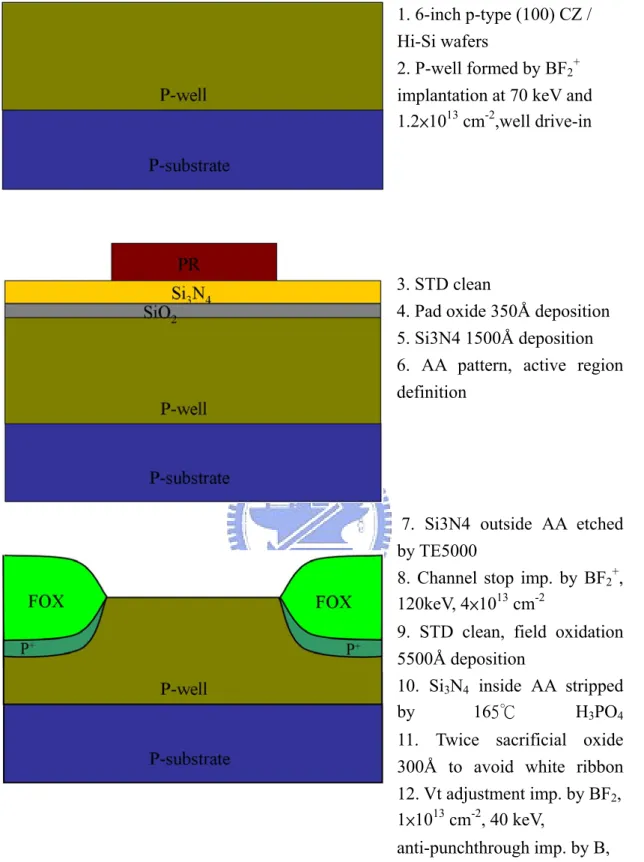
All device fabrications were carried out at National Nano Device Laboratories. Basic fabrication flow of NMOSFETs is illustrated in Fig. 2.1. The devices were fabricated on both 6-inch p-type (100) CZ-Si wafers and Hi-wafers purchased from Toshiba Co. with resistivity of 15~25Ω-cm and thickness of 655 ~ 695 μm. The p-type well was formed first by BF2+ implantation at 70 keV and 1.2×1013 cm-2. Next,
a standard local oxidation of silicon (LOCOS) process with channel stop implant (by BF2+ implantation at 120 keV and 4×1013 cm-2) was used for device isolation.
Threshold voltage adjustment and anti-punch through implantation steps were done by implanting 40 keV BF2+ and 35 keV B+, respectively. A split with an additional F+
implantation prior to the gate oxide formation was also fabricated and investigated for the possibility of improving the reliability. After the growth of 2.5 nm thick thermal gate N2O oxide, a 200nm undoped poly-Si layer was deposited by low-pressure
chemical vapor deposition (LPCVD), followed by gate etching process to pattern the poly-Si film. The source/drain (S/D) extension regions were then formed by As+ implantation at 10 keV and 5×1014 cm-2. After a 200 nm TEOS spacer formation, S/D regions were formed by As+ implantation at 30 keV and 5×1015 cm-2. Then the substrate electrode patterning was performed through lithography and etching processes, followed by the formation of the substrate contact regions by BF2+
implantation at 40 keV and 5×1015 cm-2. Rapid thermal anneal (RTA) was subsequently carried out in a nitrogen ambient at 1000°C for 10 sec to activate
dopants in the gate, S/D, and substrate regions.
Afterwards, some samples were capped with a TEOS layer to serve as the buffer layer. The thickness of the TEOS buffer layer is about 7 nm as illustrated in Fig. 2.2. Then parts of the wafers with or without the TEOS buffer layer were deposited by a Si3N4 capping layer (contact-etch-stop-layer, CESL) of 300nm, which was performed
at 780 ℃ with SiH2Cl2 and NH3 as the reaction precursors by using the low-pressure
chemical vapor deposition (LPCVD) system, while other wafers deliberately skipped the Si3N4 capping layer to serve as the controls. Then all wafers were combined to
receive a 300nm TEOS passivation layer by LPCVD system. After contact hole etching, normal metallization scheme was carried out. The final step was a forming gas anneal performed at 400°C for 30 min to mend the dangling bonds and to reduce interface state density at the gate oxide/Si interface. Cross-sectional view of a
fabricated device is shown in Fig. 2.1. NMOSFETs with different split conditions are summarized in Table 2.1.
2-2 Electrical Measurement Setup
Current-voltage (I-V) and capacitance-voltage (C-V) characteristics were evaluated by an HP4156A precision semiconductor parameter analyzer and an HP4284 LCR meter, respectively. Temperature-regulated hot chucks were used to set the measurement temperature at 25°C.
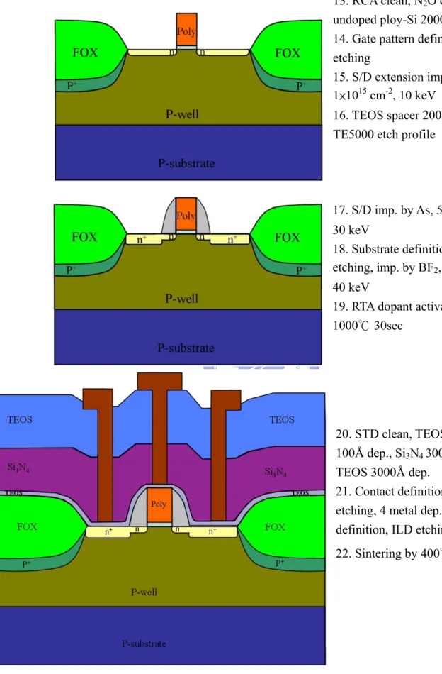
2-3 Charge Pumping Measurement Setup
2-3.1 Basic Theory
The charge pumping method was originally proposed in 1969 by Brugler and Jespers [57], where an MOSFET was used as the tester. The method is, therefore,
suitable for interface trap measurements on small-geometry MOSFETs instead of large-diameter MOS capacitors. Besides, this measurement allows the exclusion of gate leakage contribution to the calculated interface state densities existing within gate oxides [58], so we don’t need to pay attention to the leakage issue for precisely analyzing the interface state densities or the bulk traps in the gate dielectrics from the charge pumping measurement results. The basic measurement is composed of applying a small fixed reverse bias to the source/drain, connecting the substrate to ground, and performing a series of base voltage pulses with fixed amplitude, rise time, fall time, frequency, and duty cycle to the gate of the device from a low accumulation level to a high inversion level. Moreover, the maximum charge pumping current will occur when the base level is lower than the flat-band voltage and the top level of the pulse is higher than the threshold voltage. Such mechanism reveals that once the device is pulsed from inversion toward accumulation, the net charges will be transferred from the source/ drain to the substrate through the fast interface traps. The repetitive recombination at interface traps leads to the charge pumping current. Finally, the recombination current measured from the substrate is addressed as the charge pumping (CP) current [59]. An MOSFET with a gate area of AG (=W∗ L) gives the
charge pumping current as:
Icp= q∗ f∗ AG∗ Nit (2-1)
while the interface trap density (Nit) could be calculated from this equation. On the
contrary, the fast interface traps are everlastingly filled with electrons in the inversion level or holes in the accumulation level for NMOSFETs while the base level of the pulse is higher than the threshold voltage or the top level is lower than the flat-band voltage. Thus the recombination current is impossible to generate, therefore no charge pumping current can be collected.
There are three conventional types of voltage pulse train individually applying to the gate electrode, which are named as follows: (a) fixed amplitude sweep, (b) fixed base sweep, and (c) fixed peak sweep, as illustrated in Fig. 2.3. In this thesis, “fixed amplitude sweep” mode was used to calculate interface trap density while “fixed base sweep” mode was used to analyze the lateral distribution of interface trap, respectively. The basic setup of charge pumping measurement is shown in Fig. 2.4. The source and drain are both biased at 50mV while the substrate electrodes are connected to ground. Square-wave waveforms with 1M Hz provided by HP8110A are applied to the gate, and the base voltage is varied to transfer the surface condition from inversion to accumulation, while keeping the pulse amplitude at 1.5V. In our measurement setup, Vbase is varied from -2V to 0V in step of 0.05V. The parameter
analyzer HP4156A is used to measure the charge pumping current (ICP).
2-4 Hot Carrier Reliability Measurement Setup
In our reliability measurements, devices were stressed with the drain voltage set at a highly positive voltage, and the gate terminal was biased at the voltage where maximum absolute value of Isub occurred to accelerate the degradation. To find the
condition, we first measured the Isub-VG characteristics with drain terminal biased at
a given voltage. To monitor the hot electron degradation, both the ID-VG
characteristics at VDS = 50 mV (linear region) and charge pumping current were
measured before and after the stress. The degradations in terms of threshold voltage shift (ΔVth), generation of interface trap density (ΔNit), transconductance degradation
Chapter 3
Results and Discussion
3-1 Electrical Characteristics of Locally Strained
NMOSFETs with Buffer Layer
3-1.1 Basic Electrical Characteristics
Above all, this work is to discuss the impacts of inserting a TEOS buffer layer and using Hi-wafers as substrates on the performance of strained-channel NMOSFETs with Si3N4 capping layer. For brevity, we name all splits as follows,
“Hi” represents the Hi-wafer control split, “Cz-control” represents the Cz wafer control split, “SiN/Buffer/Hi” represents the Hi-wafer with TEOS buffer layer and Si3N4 capping layer, “SiN/Buffer/Cz” represents the Cz wafer with TEOS buffer
layer and Si3N4 capping layer, “SiN/Hi” represents as Hi-wafer with Si3N4 capping
layer, “SiN/Cz” represents the Cz wafer with Si3N4 capping layer, “Hi-F” represents
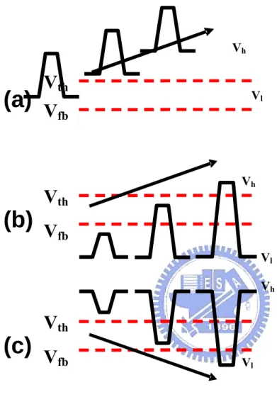
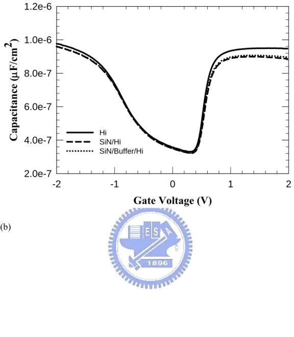
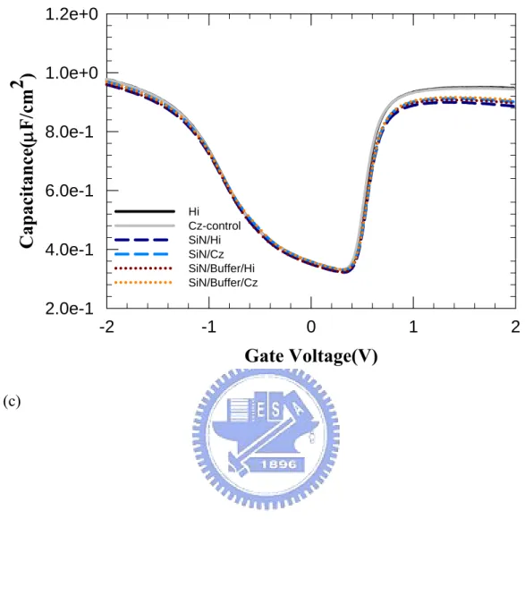
the Hi-wafer with F channel implant, “Cz-F” represents the Cz wafer with F channel implant, respectively. Figure 3.1 shows the capacitance-voltage (C-V) characteristics of devices. In the figure, we could distinctly observe that the poly-depletion effect becomes obvious in the splits with Si3N4 capping layer
depositions, irrespective of the use of Cz or Hi wafers. Based on the results of our group’s previous study [28], this is attributed to the additional thermal budget associated with the nitride deposition step. It is known that the solid solubility of dopants is temperature-dependentand the thermal conditions mentioned above tend to lower the activated carrier concentration in the poly-Si gates [62] as illustrated in Figure 3.2. Besides, the C-V characteristics of MOSFETs are very essential for
verifying the gate oxide quality and calculating the equivalent oxide thickness (EOT). Figure 3.1 (c) illustrates the C-V characteristics of NMOSFETs for all splits of samples, and the EOT, given by
inv o ox
C A
EOT =ε ⋅ε ⋅ , of those splits without Si3N4
capping layer is approximately 20.7 Å, while those splits with Si3N4 capping layer
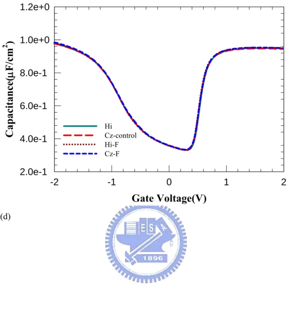
is about 22.21 Å. The difference under inversion is the direct evidence of the poly-depletion effect. Figure 3.1 (d) shows the C-V characteristics of NMOSFETs for the F-channel-implanted splits, there is no obvious difference between them, indicating the F channel implant would not influence the fundamental performance and EOT of devices.
The drain current (ID) versus gate voltage (VG) characteristics and the
transconductance (Gm) versus gate voltage characteristics of all splits with
m m L W μ μ 5 . 0 10
= @ VD =0.1V for nMOSFETs are illustrated in Figure 3.3. We
found that the subthreshold slope is higher and the off-state leakage current is also about two orders larger for the splits with Si3N4 capping layer. However, there is a
significant increase in transconductance for the splits with Si3N4 capping layer due
to the inducedtensile stress in the channel, which in turn could enhance the electron mobility. In addition, ID and transconductance (Gm) versus VG characteristics of the
splits with F-implanted channel for both Cz and Hi-wafers are illustrated in Figure 3.4. From the figure, there is no obvious difference in the off-state leakage current and the subthreshold slope among the splits irrespective of F implantation, while a slight difference approximately 3.6% could be observed at Gm,max. Therefore, it seems that the F ion implantation draws no major influence on the fundamental properties of the devices. The output characteristics of all splits with
m m L W μ μ 5 . 0 10
= , VG −Vth =0.4~2V, Step=0.8V are shown in Figure 3.5. There is no obvious difference between Cz and Hi-wafers, and it is seen that the
insertion of the TEOS buffer layer prior to the Si3N4 capping layer deposition would
not degrade the drive current enhancement caused by the capping of thicker Si3N4
etch-stop layer which is tensile inherently [63].
Figure 3.6 shows the distribution of the subthreshold slope (S.S.) versus the gate length of the F-free split conditions. For the splits of Cz-controls and Hi, S.S. is independent of gate length, and further Hi split depicts lower S.S. than Cz-controls, demonstrating that it has better interface quality due to the high temperature hydrogen anneal.However, the splits with Si3N4 capping layer depict higher S.S
than those without the SiN capping, especially when the device channel length becomes longer. The root cause forsuch phenomenonis not clear yet at this stage. Increase in EOT due to poly depletion effect may play a role. It is noted that the TEOS buffer layer could effectively block hydrogen molecules diffusion from Si3N4
capping layer deposition. As a consequence, the S.S. increases due to less effective interface passivation.Furthermore, the distribution of the S.S. versus the gate length of the F-implanted split conditions is illustrated in Figure 3.7. Again, the impact of F implant on the S.S. of the fabricated devices is not significant.
Figure 3.8 shows the percentage increase of the transconductance (Gm) among different splitswith respect to the Cz-control split as a function of channel length. The transconductance enhancement reaches about 20% at a channel length of 0.5μm. When the channel length is scaled to less than 1μm, the Gm increases sharply owing to the aforementioned strain effect. In other words, the strain is distributed locally inside the channel region and concentrated near the source and drain region. This effect can be explained by the splitting of the degeneracy at the conduction band edges under the uniaxial strain [64]. Figure 3.9 exhibits the percentage increase of Gm among the F-implanted splits with respect to the Cz-control split as a function of channel length. There is a negative percentage increase in Gm of the Cz-F split,
which may result from the implantation-induced damages, and an increase in the interface traps, which may degrade the carrier mobility. On the contrary, no obvious difference of the Gm percentage increase between the Hi and Hi-F splits is observed. Figure 3.10 exhibits the percentage increase of the on- current among different splitswith respect to the Cz-control split as a function of channel length. In this figure, it can be seen that the trend of on-current enhancement is the same as that of Gm enhancement as shown in Figure 3.8. The percentage increase of the on-current among the F-implanted splitswith respect to the Cz-control split as a function of channel length is illustrated in Figure 3.11, showing similar trend as that of Gm enhancement in Figure 3.9.
Figure 3.12shows the charge pumping current (Icp) versus the base voltage. The device size is m m L W μ μ 5 . 0 10
= , the pulse amplitude is 1.5V, and a gate voltage train of square waveform is used for Icp extraction. From the figure, the splits of SiN/Cz and SiN/Hi depict slightly higher Icp as compared with the splits of Hi and Cz-control. We discover that a large amount of the interface states are produced during the Si3N4 capping layer deposition as compared with the devices without the
Si3N4 capping layer, revealing that the channel strain certainly leads to the increase
of the interface states at the Si/SiO2 interface. But at the same time, the hydrogen
species contained in the nitride layer can effectively passivate the dangling bonds at the Si/SiO2 interface. For deposition of the LPCVD- Si3N4, SiH2Cl2 and NH3 were
used as the reaction precursors, and a significant amount of hydrogen may be incorporated in the deposited film. However, the above results indicate that the number of interface states passivated by the hydrogen species is less than that generated by the channel strain. Moreover, the charge pumping current increases doubly for the splits of SiN/Buffer/Cz than the SiN/Cz and SiN/Hi splits. These
results indicate that the TEOS buffer layer can effectively block the diffusion of hydrogen species into the channel region during the Si3N4 capping layer deposition
process.As a result, the incorporation of hydrogen species in the gate oxide and at the interface can be suppressed remarkably with the insertion of TEOS buffer layer, and the strain-induced interface trap states from the Si3N4 capping layer will not be
effectively passivated. This explains why the percentage increase of Gm for the SiN/Buffer/Cz splits is lower than that for the SiN/Cz splits. Nevertheless, it is noted that the Icp of the SiN/Buffer/Hi splits is only slightly higher thanthat of the SiN/Hi split.Therefore, the blocking of hydrogen diffusion is not a serious concern for the SiN/Buffer/Hi splits. The Icp versus base voltage for the F-implantated splits is illustrated in Figure 3.13. As can be seen in the figure, we find that the Icp of the F-implant split is much higher than that of other splits, owing to the implant damages in the channel region, consistent with the trend of the percentage increase of the Gm.
Figure 3.14 shows the comparison of the effective mobility extracted from the split C-V method among different split of samples. The device size is
m m L W μ μ 50 50
= . The splits of Cz group depict degraded behaviors for the splits with the Si3N4 capping layer in the low field region, as shown in Figure 3.14(a).
This indicates that the higher interface states tend to enhance the Coulomb scattering mechanism. On the other hand, from the splits of Hi group, it is very interesting to note that the TEOS buffer layer will not cause the mobility degradation, as shown in Figure 3.14(b).Figure 3.15 exhibits the distribution of the on-current (VG=1.8V, VD=1.8V) versus off-current (VG=0V, VD=1.8V). From the
figure, we can find that the splits fabricated with the Hi-wafers possess lower off- current than the splits fabricated with the Cz wafers, due to inherently better surface
quality of Hi-wafers.
3-1.2 Short Channel effects
Threshold voltage (VTH) roll-off characteristics for all splits of devices are
illustrated in Fig. 3.16, in which the value of VTH
( )
L −VTH(
10μm)
is plotted as afunction of gate length. The results are obtained at VDS = 0.1 V. Among the splits,
both the Hi split and the Cz-control split depict a pronounced reverse-short-channel-effect (RSCE). This can probably beexplained by the boron segregation at the implant-damaged regions located close to the edge of the channel [65]. However, the phenomenon of the RSCE is not observed in the SiN-capping splits (both Cz and Hi-wafers), due to two mechanisms described as follows: First, the additional thermal budget of the nitride deposition helps redistribute the segregated boron atoms. Second, the bandgap narrowing effect caused by the induced strain has been shown to be one of the culprits to accelerate the threshold voltage roll-off in the strained channel devices [49,66]. Moreover, strain likely also leads to the channel dopants redistribution [67,68]. In brief, the channel strain associated with the SiN-capping splits of both Cz and Hi-wafers would result in the aggravated Vth roll-off. Furthermore, Figure 3.17 shows the distribution of threshold voltage roll-off characteristics of the F-implanted splits versus the gate length. From the figure, we find that all splits exhibit obvious reverse-short-channel-effect due to no extra thermal budget. However, the Cz-control split shows a slightly larger VTH shift over the Cz-F
split, and such slight VTH shift difference may result from F atoms enhancing boron
diffusion, similar to the situation of the Si3N4-capping devices as mentioned above.
On the contrary, the Hi-F split exhibits sightly higher VTH shift over the Hi split,
susceptible to the oxidation-enhanced-diffusion (OED) and than the Cz-F split, [69] so boron would not diffuse as seriously as in the case of the Cz-F split owing to the assistance of the OED effect.
Drain induced barrier lowing (DIBL) is another indicator in evaluating the short channel effects. We use the interpolation method to calculate DIBL effect for all splits of samples. The results are shown as a function of channel length in Fig. 3.18. It is clearly seen that there is no distinguishable difference among all splits. It appears that the devices with Si3N4 capping layers and buffer layers will not worsen the DIBL
effect of the samples. In addition, Fig. 3.19 exhibits the DIBL characteristics for the F-implanted splits as a function of channel length. From the figure, we can find that a distinct gap exists between the F-implanted splits and the F-free splits, indicating that F atoms indeed enhance boron diffusion and lead to worse short-channel-effect (SCE) degradation.
3-2 Hot Carrier Degradation of Locally Strained
NMOSFETs with Buffer Layer
A hot carrier with sufficient energy can create more charge carriers through impact ionization. For NMOSFET devices, holes generated by impact ionization are collected by the substrate. The substrate current (Isub) versus gate voltage for all splits
of devices at VDS of 3.75 V is illustrated in Fig.3.20. From the figure, we can clearly
see that the Si3N4-capped splits exhibit larger substrate current than the control splits
for both Cz and Hi-wafers. Such phenomenon is closely related to the channel strain. Bandgap narrowing and carrier mobility enhancement by the channel strain are the two major contributors to the enhancement of the ionization rate [70,71]. As a consequence, the SiN-capped devices show larger substrate current than the control
samples. In addition, among the SiN-capped splits, the SiN/Buffer/Hi split exhibits the largest Isub owing to its largest transconductance. Besides, Fig. 3.21 shows substrate current versus gate voltage for the F-implanted splits at VDS of 3.75 V. It can
be seen that devices with F-implant depict smaller Isub than F-free splits. Possible explanation for this phenomenon is the extra defects induced by F implant which may act as scattering centers for energy relaxation during the carrier transport process. Hot-carrier effects and associated performance degradation were investigated to evaluate the impacts of Si3N4 capping layer, the TEOS buffer, and the F ion
implantation. It is expected that the nitride-capped splits will exhibit aggravated hot carrier degradation as mentioned above. Threshold voltage shift and interface state density increase as a function of stress time for all splits of samples are shown in Figs. 3.22 and 3.23, respectively, after receiving a hot-electron stressing at VDS = 3.75 V
and VGS at the maximum absolute value of substrate current. All devices are with
channel width/length = 10μm/0.5μm. The SiN-capping splits for both Cz and Hi-wafers exhibit the worst hot-carrier degeneration, while the improvement of the hot-carrier degradation by using the TEOS buffer layers is obviously seen. However, the threshold voltage shift of the SiN/Hi split is worse than that of the SiN/Cz split, similar to the case of the buffer-layer splits, owing to the fact that thefresh maximum Gm values of both the SiN/Hi split and the SiN/Buffer/Hi split are larger than that of the SiN/Cz and the SiN/Buffer/Cz splits.
It is important to note that, although the substrate current is high for the SiN/buffer samples, significant improvement in HC resistance than that without the buffer is observed. Since the hot carriers tend to break the Si-H bonds during the stressing, and much severe degradation will occur with higher Si-H density. The use of TEOS buffer layer can effectively block the diffusion of hydrogen species into the channel region, therefore less HC degradation in terms of Vth shift and interface-state
generation is achieved.
Figures 3.24 and 3.25 depict threshold voltage shift and increased interface state density, respectively, as a function of stress time for F-implanted splits, measured at VDS = 3.75 V and VGS at the maximum absolute value of substrate current. From the
figures, we can distinctly see that the F-implanted splits show smaller threshold voltage shift and less Nit increase than the F-free splits, similar to the distribution of the substrate current, indicating F ion implantation indeed improves the reliability issues of NMOSFETs. At the same time, there is an interesting discovery that the Cz-F split is always better than the Hi-F split on the performance, possibly due to the oxidation-enhanced-fluorine-diffusion effect as mentioned above, in which the oxygen-rich Cz-F split will tend to have more fluorine atoms diffusing downward to the channel region below or upward to the gate oxide to strengthen the bondings. Therefore, the strengthened bondings lead to alleviated hot-carrier degradation. In addition, the transconductance degradation is another indicator to judge the hot-carrier effect. Figures 3.26 and 3.27 illustrate the transconductance degradation after the hot-electron stressing performed at VDS=3.75V and VGS at the maximum substrate
current for the SiN-capped and the F-implanted splits, respectively. Devices with channel width/channel length = 10μm/0.5μm were characterized. In Fig. 3.26, the SiN/Hi split shows the worst Gm degradation over other splits due to the strain enhancement effects and extra hydrogen incorporation mentioned above. On the other hand, the OFD effect of the F ion implantation and inherently better surface quality of the Hi-wafers are used to interpret the whole Gm degradation distribution of Fig. 3.27. Typical results of hot-electron stressing for the F-free splits of devices on the Hi-wafers and Cz wafers are shown in Figs. 3.28 and 3.29, respectively. Channel width and length of the test devices are 10μm and 0.5μm, respectively. The devices are stressed at VDS = 3.75 V and VGS at maximum absolute value of substrate current.
The ID-VG characteristics at VDS = 0.05 V are measured before and after the stress to
evaluate the degradation caused by the hot electrons. In the figures it is observed that the degradation is the worst in the SiN-capped sample without buffer layer among the six splits studied. The aggravation is alleviated in the devices with TEOS buffer layer, though the resultant degradation is still worse than that of the control splits. In addition, Fig. 3.30 exhibits the basic electrical characteristics of hot-electron stressing for the F-implanted splits of devices built on either Hi-wafers or Cz wafers. Still, the F ion implantation improves the hot-carrier reliability as explained above. The increase in charge pumping current after 5000 s of hot carrier stress is shown in Fig. 3.31. The effect of the TEOS buffer layer is observed in terms of lower Icp than the△ buffer-free devices. After stressing, the SiN/Buffer/Hi split possesses higher Icp △ than the SiN/Buffer/Cz split, although in principle the former split should have a better interface quality. Higher substrate current and higher population of generated hot carriers are postulated as the plausible origin for this observation. On the contrary, Fig. 3.32 illustrates the increase in stressed charge pumping current for the F-implanted splits of devices. There is no contradiction existing between the Icp △ and the aforementioned results.
Chapter 4
Summary and Conclusions
In this thesis, the effects of both the Si3N4 layer capping over the gate and the
hydrogen-blocked TEOS buffer layer inserted prior to the Si3N4 deposition, on the
NMOS device characteristics as well as the correlative hot-electron degradation were investigated. The devices were built on two kinds of the substrates, namely, Cz and Hi-wafers. Besides, the influences of the F channel implant on both fundamental performance and the related reliability of the fabricated devices were also explored. Several important findings were obtained and summarized as follows.
(1) For devices on the Hi-wafer, the buffer layer would not degrade the device performance. For examples, the enhancement ratio of transconductance for the devices of SiN/Buffer/Hi split at a channel length of 0.5μm is 20%, comparable to 19% of the SiN/Hi split at the same channel length. On the contrary, the buffer layer for devices built on Cz wafers would degrade the performance. Enhancement ratio of transconductance for the SiN/Buffer/Cz split at a channel length of 0.5μm is lowered to 11% from 15% of the SiN/Cz split. Such disparity is attributed to the better surface quality of the Hi wafers. On the other hand, the F channel implant draws significant impacts on the device performance for devices built on Cz wafers, such as degradation of Gm and S.S. When Hi wafers were used as the starting substrates, such negative impacts could be relaxed. These findings highlight the merits of Hi wafers over that of Cz wafers.
(2) The thermal budget associated with the deposition of the Si3N4 capping layer
could help redistribute the segregated boron dopants in the channel and alleviate the reverse short-channel effect, although the poly-depletion effect becomes worse. The
bandgap narrowing effect due to the channel strain may result in further lowering in VTH as the channel length is shortened.
(3) The TEOS buffer layer could effectively block the diffusion of hydrogen species from Si3N4 into the channel and interface of Si/SiO2 during the Si3N4
deposition and subsequent thermal cycles.
(4) The hot-electron degradation is adversely affected when the Si3N4 capping
layer is deposited over the gate as compared with the control samples, regardless of the types of wafers. When a TEOS buffer layer was inserted prior to the Si3N4
deposition, although still worse than the control ones, significant improvement in resistance to the hot-carrier degradation over that without buffer is achieved.
(5) The hot-electron degradation could be improved by the F channel implant. In this aspect, the Cz wafer-split with the F-implant possesses the most significant improvement in resisting the hot-electron degradation. This is ascribed to the stronger Si-F bonds at the interface by the OED effect for the Cz wafers, even the split with the worst fresh performance. This result implies the only demerit of the purpose of Hi-wafer when collocated with the F-implant.
In this work, we found that hydrogen species is the primary culprit for the aggravated reliabilities in the strained devices. The insertion of a buffer layer has been shown to be effective in this work to alleviate the associated hot-carrier degradation. The usages of both Hi-wafer and F channel implant ought to be treated carefully to optimize both device characteristics as well as hot-carrier reliability. Optimization of Si3N4 deposition conditions, search of other suitable materials for buffer layer, and use
of different wafer orientation are possible ways for further improving the characteristics of devices implemented with uniaxial channel strain.
References:
[1] P. K. Bondyopadhyay, “Moore’s Law Governs The Silicon Revolution”, IEEE Trans. Electron Devices, Vol. 86, pp.78-81, Jan.1998.
[2] S. H. Olsen, K. S. K. Kwa, L. S. Driscoll, S. Chattopadhyay, and A. G. O’Neill, “Design, Fabrication and Characterization of Strained Si/SiGe MOS Transistors”, IEE Proc.-Circuits Devices Syst., Vol. 151, No. 5, October 2004.
[3] S. M. Sze, “Physics of Semiconductor Devices”, Second Edition, pp.469-486, 1985.
[4] Yuan Taur, Tak H. Ning, “Fundamentals of Modem VLSI Devices”, pp.161, 187, First published 1998, Reprinted 1999.
[5] D. A. Buchanan, and S. -H. Lo, “Reliability and Integration of Ultra-Thin Gate Dielectrics for Advanced CMOS”, Microelectron, Eng., pp.13-20, 1997.
[6] H. S. Momose, M. Ono, T. Yoshitomi, T. Ohguro, S. –I. Nakamura, M. Saito, and H. Iwai, “1.5nm Direct-Tunneling Gate Oxide Si MOSFETs”, IEEE Trans. Electron Devices, vol. 43, pp.1233, Aug. 1996.
[7] L. Manchanda, W. H. Lee, J. E. Bower, F. H. Baumann, W. L. Brown, C. J. Case, R. C. Keller, Y. O. Kim, E. J. Laskowski, M. D. Morris, R. L. Opila, P. J. Silverman, T. W. Sorsch, G. R. Weber, “Gate Quality Doped High K Films for CMOS Beyond 100 nm: 3-10 nm Al2O3 with Low Leakage and Low Interface
States”, IEDM Technical Digest, pp. 605, 1998.
[8] E. P. Gusev, M. Copel, E. Cartier, I. J. R. Baumvol, C. Krug, M. Gribelyuk, “High-Resolution Depth Profiling in Ultrathin Al2O3 Films on Si”, Appl. Phys.
Lett. Vol. 76, pp. 176, 2000.
[9] M. Copel, E. Cartier, E. P. Gusev, S. Guha, N. Bojarczuk, M. Poppeler, “Robustness of Ultrathin Aluminum Oxide Dielectrics on Si (100)”, Appl. Phys.
![Fig. 1.1 Gate length scaling as a function of the year of introduction for technology node [2]](https://thumb-ap.123doks.com/thumbv2/9libinfo/8645583.193542/53.892.135.664.176.769/fig-gate-length-scaling-function-year-introduction-technology.webp)
![Fig. 1.3 Simple schematic of conduction and valence band bending with strain [47].](https://thumb-ap.123doks.com/thumbv2/9libinfo/8645583.193542/55.892.140.715.115.453/fig-simple-schematic-conduction-valence-band-bending-strain.webp)
![Fig. 1.6 Schematic diagram of the oxygen depth profile after hydrogen anneal at 1200℃ for 1 hour [52]](https://thumb-ap.123doks.com/thumbv2/9libinfo/8645583.193542/56.892.136.758.507.1082/fig-schematic-diagram-oxygen-depth-profile-hydrogen-anneal.webp)